Chapter 4
Characterization of Conducted
Emissions in Time Domain
Contents of this chapter
4.1 Introduction . . . 53
4.2 Theory of signal processing . . . 55
4.2.1 Discrete Fourier transform . . . 55
4.2.2 Windowing . . . 55
4.2.3 Time-frequency analysis . . . 56
4.3 Measurement system . . . 57
4.3.1 Measurement methodology . . . 57
4.3.2 Experimental validation . . . 59
setup selection . . . 59
Validation of the characterization via time-domain measurements . . . 59 4.4 Characterization of electric devices with non-stationary emissions 61
4.1
Introduction
standards, what entails some disadvantages, as for instance, low precision with the measurement of non-stationary emissions. An alternative way of proceeding is to perform the conducted emissions measurement in the time domain, recovering the frequency components by further signal processing. The advantages of time-domain measurements in front of frequency-domain measurements are:
- Faster measurements: a VSA has to measure all the frequency range (150 kHz-30 MHz) using a narrow resolution bandwidth (RBW) (9 kHz, [12]), that involves slow measure-ments (specially if the quasi-peak and average detectors are used). Using a high-speed time sampling, it is possible to capture the signal in the time domain and compute its spectral components in a shorter time period [8], [105]–[109].
- Better precision with non-stationary emissions: since the measurement of the conducted emissions with a VSA is performed moving its 9-kHz RBW through the frequency range in several frequency steps, different frequencies are measured at different times. If the signal shows repeating events, the measurement time must be set long enough to ensure that at least one event of interest falls into the dwell time of each frequency step. In the case of a one-time transient, only a single frequency can be measured. This problem can be solved if the event is captured in the time domain, since all the frequencies are measured simultaneously [105], [106].
- The measurements performed by a VSA (peak, quasi-peak, average and phase) can also be obtained by simulating the different detectors via computation. Besides, further in-formation not given by a VSA can be obtained, such as the statistical properties of the interference signal [8], [20], [109]–[114].
- Simpler measurement devices: it is easier to find a channel oscilloscope than a two-channel VSA, and the cost of an oscilloscope is usually cheaper than the VSA one [13], [20], [106], [107].
Therefore, time-domain analyzers seem to be the best choice for the conducted emissions measurements, especially for DUTs with non-stationary emissions. On the other hand, it must be considered that the time domain approach presents a limited dynamic range due to the quantization error [106]. For instance, an 8-bit oscilloscope has a theoretical dynamic range of about 48 dB while SAs usually present a dynamic range above the 80 dB. This is the main reason for what most of the EMC labs still measure the conducted emissions in the frequency-domain despite all the advantages of time-frequency-domain measurements presented above.
4.2 Theory of signal processing 55
noise. The model obtained is finally validated by comparing its simulated conducted emissions with the ones measured with a SA. In the fourth section, the methodology is used to characterize a DUT with non-stationary noise, showing that time-domain measurements are very useful when frequency-domain measurements cannot be applied.
4.2
Theory of signal processing
4.2.1 Discrete Fourier transform
The digitization of a continuous-time signal x(t) with a sampling frequency fs (that
cor-responds to a sampling interval ∆t = 1/fs) leads to the discrete-time signal x[n], where x[n] = x(n∆t). Shannon’s theorem requires fs to be at least twice as high as the maximum
signal frequency [105]. Ifx[n] is a data block ofN samples, its spectral estimation is obtained via the discrete Fourier transform (DFT) [115]:
X[k] =
N−1 X
n=0
x[n]e−j2πknN with 0≤k < N (4.1)
The DFT transforms the discrete-time signal sequence x[n] into the discrete-frequency spectral sequenceX[k], withk denoting the discrete frequency intervalX[k] =X(k∆f). Due to the basic properties of the DFT, the relation between ∆t,N and ∆f is:
∆f = 1
N∆t (4.2)
The DFT of a time-domain sampled waveform is a symmetric function which becomes redundant beyond the Nyquist frequency (fs/2). Therefore, the spectral information can be
evaluated from only one half ofX[k], but its magnitude has to be multiplied by two in order to balance the signal energy of the other half. Besides, the DFT has to be normalized by the number of time-domain samplesN in order to obtain results analogous to the continuous Fourier transform, and divided by √2 (for k > 1) to compute the root mean square (RMS) values [105]. Joining all the scaling factors and obviating the direct-current (DC) component (X[0]), the following definition is obtained:
X[k] =
√
2 N
N−1 X
n=0
x[n]e−j2πknN with 1≤k < (
N
2 for N even
N+1
2 for N odd
(4.3)
4.2.2 Windowing
xw[n] =x[n]w[n] , 0 ≤n < N (4.4)
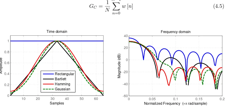
The weighting function is chosen to smoothly roll off to zero the edge points of the signal in time domain. This is equivalent to convolute the signalX[k] with a function whose side lobes have lower amplitude than the square window ones. Figure 4.1 shows some popular weighting functions in time and frequency domain. As can be seen, the improvement in the leakage comes as a trade-off against frequency resolution and energy. However,w[n] can be scaled to make its integral over the observation interval ∆TN equals the unity with a scaling factor called coherent
gain (GC) [116]:
GC =
1 N
N−1 X
n=0
w[n] (4.5)
10 20 30 40 50 60
0 0.2 0.4 0.6 0.8 1
Samples
Amplitude
Time domain
0 0.05 0.1 0.15 0.2
-60 -40 -20 0 20 40
Normalized Frequency (×π rad/sample)
Magnitude (dB)
Frequency domain
[image:4.595.69.518.299.511.2]Rectangular Bartlett Hamming Gaussian
Figure 4.1: Different window functions.
Due to the linearity of the DFT, the scalar factorGC can be applied after the transformation
into the frequency domain:
Xw[k] =
√
2 GCN
N−1 X
n=0
xw[n]e−
j2πkn
N with 1≤k < (N
2 for N even
N+1
2 for N odd
(4.6)
Different choices of window functions present different compromises between leakage sup-pression and spectral resolution.
4.2.3 Time-frequency analysis
4.3 Measurement system 57
samples, satisfyingN ≥Lands≤N (so that each block is overlapped byN−ssamples), and computes the DFT of each block to obtainX[n′, k], which depends of the time shiftn′ and the
frequencyk:
Xw
n′, k
=
√
2 GCL
L−1 X
m=0
x
sn′+m
w[m]e−j
2πkm N
with 1≤k <
(
N
2 for N even
N+1
2 for N odd
and 0≤n′< N−L s
(4.7)
The observation timeTob, the time resolution ∆tST F T and the frequency resolution ∆f are
given by:
Tob=
N −L fs
∆tST F T = s fs
=s∆t ∆f = 1
L∆t (4.8)
The choice of the window length and the number of overlapping samples becomes a trade-off between frequency and time resolution.
4.3
Measurement system
4.3.1 Measurement methodology
The methodology to characterize a DUT consists of the following steps:
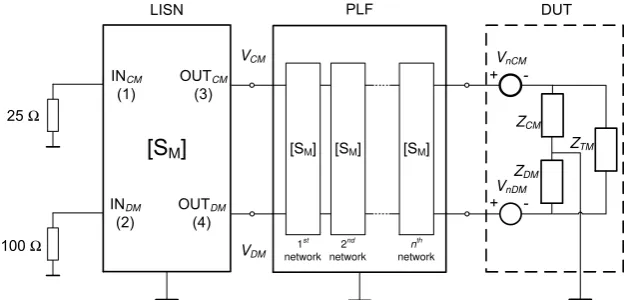
1. Measurement of the scattering (S) parameters of the DUT at its line (L) and neutral (N) ports as it was explained in chapter 3. The impedances ZL, ZN and ZT are obtained
with (3.1).
2. Measurement of the conducted emissions in time domain. Figure 4.2 shows two possible setups for the conducted emissions measurements in time domain: in figure 4.2(a) the conducted emissions are measured using two current probes on L and N terminals, a similar setup to the one used in [120] for the conducted emissions measurements of a DC-DC converter; in figure 4.2(b) the conducted emissions are measured after the line impedance stabilization network (LISN), as it was done in the previous chapter with the VSA.
After measuring the conducted emissions in time domain, the spectral components are computed using (4.6). However, the information obtained in each scenario is different:
- From the measurement setup of figure 4.2(a), the currents at the terminal portsIL
andIN are obtained. Considering the equivalent circuit of the measurement system
VBL VBN PL PL dev dev mon mon VL VN
VBL VBN IL IN PL PL dev dev mon mon
Figure 4.2: Two possible setups for the conducted emissions measurements in time domain via (a) current measurements or (b) voltage measurements.
expressions:
VL = IL
Z0SS3434SS4343−−((SS3333−+1)(1)(SS4444−−1)1)
+IN
Z0S34S43−(S233S34−1)(S44−1)
VN = IN
Z0SS3434SS4343−−((SS3333−−1)(1)(SS4444+1)−1)
+IL
Z0S34S43−(S233S43−1)(S44−1)
(4.9)
where Z0 is the reference impedance of the measurement system. Once the VL and VN voltages are found, the interference voltage sourcesVnLandVnN can be obtained
using (3.3).
- From the measurement setup of figure 4.2(b), the voltages at the terminal ports of the oscilloscope VBL and VBN are obtained. The VL and VN voltages can be
recovered by using (3.8), and the interference voltage sources VnL and VnN with
(3.3). IL andIN can also be obtained with the following expressions:
IL = VZL0
S34S43−(S33−1)(S44+1)
S34S43−(S33+1)(S44+1)
+VN
Z0
−2S34
S34S43−(S33+1)(S44+1)
IN = VZN0
S34S43−(S33+1)(S44−1)
S34S43−(S33+1)(S44+1)
+VL
Z0
−2S43
S34S43−(S33+1)(S44+1)
(4.10)
whereZ0 is the reference impedance of the measurement system.
3. Finally, having found all the values of the circuit-model components (ZL, ZN, ZT, VnL
4.3 Measurement system 59
4.3.2 Experimental validation
setup selection
In order to determine the most appropriate setup of figure 4.2, both scenarios have been used to perform the time-domain conducted emissions measurements on different switching power supplies as the one of figure 4.3. The measurement settings applied for an optimal capture are: fs = 500 MSps, which corresponds to a ∆t= 2 ns, and low-pass filtering with a
cut-off frequency of 250 MHz; the storage length is of 1 MS, leading to a ∆f = 500 Hz and a Nyquist frequency of 250 MHz. The frequency components are obtained computing (4.6) with the Fast Fourier Transform (FFT) algorithm [115].
Figure 4.3: Switching power supply connected to several loads.
Figure 4.4 shows the currents at the L and N terminals of one of the switching power supplies, measured with the setup of figure 4.2(a) (using two Tektronix TCP0030 current probes with a current sensitivity of 1 mA) and the setup of figure 4.2(b). When the setup of figure 4.2(a) is used, the low frequency is not filtered and the spectral components of the 50-Hz windowed signal masks the conducted emissions of the switching power supply. To reduce this effect, the 50-Hz signal is filtered by applying detrending techniques [121]. As can be seen, both measurement setups present similar peak frequency results, but the setup of figure 4.2(b) presents a better sensitivity. Until now there is not any current probe available in the market with the same frequency span and better sensitivity, which means that it is not possible to get better results from current measurements without using further external devices. Therefore, the setup of figure 4.2(b) has been selected to validate the DUT characterization with time-domain measurements.
Validation of the characterization via time-domain measurements
To validate the characterization of a DUT with conducted emissions via time-domain mea-surements, the complete characterization of a switching power supply has been performed. The circuit model obtained has been simulated using the circuit of figure 4.5, where the LISN is represented through itsS parameters.
106 107 -30
-20 -10 0 10 20 30
Frequency (Hz)
Mag I
L
(dBuA)
106 107
-30 -20 -10 0 10 20 30
Frequency (Hz)
Mag I
N
(dBuA)
I measured with OSC I measured with probes
Figure 4.4: Spectrum of theILandIN currents measured with both setups of figure 4.2.
mon
mon
dev
dev
VL
VN
ZL
VnL
ZT
ZN
VnN
4.4 Characterization of electric devices with non-stationary emissions 61
Figure 4.6 shows the simulated and measured conducted emissions of the switching power supply. The good agreement between them proves that time-domain measurements are useful to characterize this kind of DUT. Besides, while the conducted emissions measurement in the frequency domain lasts about ten minutes, the same measurement in time domain and post processing spends only twenty seconds, showing an advantageous reduction of time.
106 107
0 10 20 30 40 50 60
Frequency (Hz)
Mag V
L
(dBuV)
106 107
0 10 20 30 40 50 60
Frequency (Hz)
Mag V
N
(dBuV)
Simulated Measured
Figure 4.6: Comparison between simulated and measured conducted emissions of a switching power supply.
4.4
Characterization of electric devices with non-stationary
emis-sions
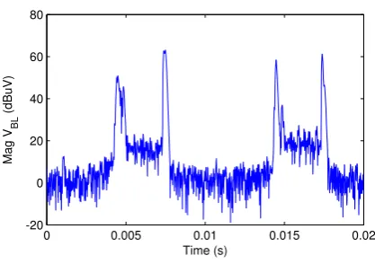
Time-domain measurements have been proved to be useful in terms of time saving when they are applied on the characterization of DUTs with stationary interference. In this section, the same methodology is tested to study its performance when the DUT presents non-stationary interference. Figure 4.7 shows the conducted emissions at the L and N terminals of a switching power supply obtained with the three EMI detectors of a SA [12]: peak, quasi-peak and average detector. As can be seen, the peak and quasi-peak detectors show a wide-band interference which spans from 150 kHz to 30 MHz. However, this emission is not detected with the average detector. This is only explained due to the non-stationary nature of the wide-band interference, as can be seen in figure 4.8, which shows the conducted emissions measured with the SA at the frequency of 200 kHz and zero-span. The interference is only present a few times during the 50-Hz period.
106 107 -20
0 20 40 60 80
Frequency (Hz)
Mag V
L
(dBuV)
106 107
-20 0 20 40 60 80
Frequency (Hz)
Mag V
N
(dBuV)
[image:10.595.185.394.529.676.2]Peak detector Quasi-peak detector Average detector
Figure 4.7: Conducted emissions of a switching power supply with the three EMI detectors: peak, quasi-peak and average detector.
0 0.005 0.01 0.015 0.02 -20
0 20 40 60 80
Time (s)
Mag V
BL
(dBuV)
4.4 Characterization of electric devices with non-stationary emissions 63
ZL,ZN and ZT and the two noise sourcesVnL andVnN, is obtained, it can be simulated using
the circuit of figure 4.5. Figure 4.10 shows the comparison between the simulated conducted emissions of the equivalent model and the conducted emissions measured with the peak detector. As can be seen, both spectra are completely different, since the windowed time-domain signal is long enough to smooth the spectral components of the impulsive noise.
0 0.5 1 1.5 2
x 10-3
-0.04 -0.02 0 0.02 0.04 0.06 0.08 Time (s) VBL (V)
0 0.5 1 1.5 2
x 10-3
-0.08 -0.06 -0.04 -0.02 0 0.02 0.04 Time (s) VBN (V)
Figure 4.9: Conducted emissions of the switching power supply measured in time domain.
106 107
10 20 30 40 50 60 70 80 Frequency (Hz) Mag V L (dBuV)
106 107
10 20 30 40 50 60 70 80 Frequency (Hz) Mag V N (dBuV) Real emissions Model emissions
Figure 4.10: Comparison between the simulated conducted emissions and the conducted emissions measured with the peak detector.
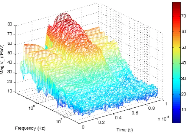
In order to visualize the spectra disturbance when the transient appears, the STFT has been applied on the central 0.5 MS of the conducted emissions data at the L terminal (VL),
using a window length of 50000 samples and a step size of 7000 samples. The three-dimensional information is shown in figure 4.11, where the frequency resolution is of 10 kHz, time resolution of 14µs and a total observation time of 0.9 ms. An increase of the spectral noise can be seen between the 0.4 and 0.6 ms, similar to the spectrum measured with the peak detector (figure 4.7).
Figure 4.11: STFT of the conducted emissions at the L terminal (VL).
only the samples that contain the impulsive interference, that is, those placed between the 0.4 and 0.6 ms. The simulation results are shown in figure 4.12, obtaining now a good agreement with the peak-detector measurements. The results obtained show that the impulsive noise of a DUT can be characterized using time-domain measurements.
106 107
10 20 30 40 50 60 70 80
Frequency (Hz)
Mag V
L
(dBuV)
106 107
10 20 30 40 50 60 70 80
Frequency (Hz)
Mag V
N
(dBuV)
[image:12.595.124.435.130.350.2]Simulated emissions Real emissions
Figure 4.12: Comparison between the simulated conducted emissions and the conducted emissions measured with the peak detector.
4.4 Characterization of electric devices with non-stationary emissions 65
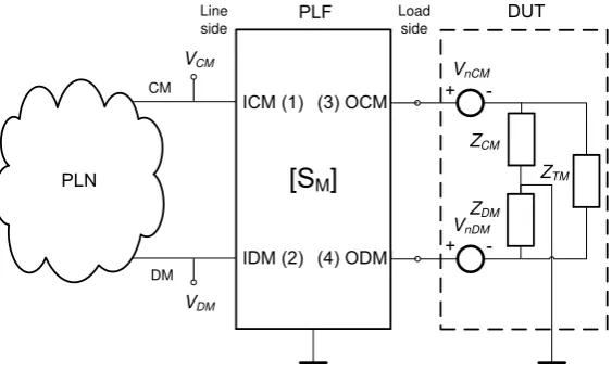
is the DM, which exceeds the circuit limit for 20 dB at low frequencies. Therefore, a suitable power-line filter (PLF) for this device has to be composed, at least, by an X capacitor, in order to mitigate the DM emissions. This fact shows that the modal simulation provides useful information for filtering design methodologies.
CM
DM
CM
DM
VCM
VDM
VnCM
VnDM
ZCM
ZDM
ZTM
Figure 4.13: Simulation of the modal conducted emissions of a DUT.
106 107
-20 0 20 40 60 80 100
Frequency (Hz)
Mag V
CM
(dBuV)
106 107
-20 0 20 40 60 80 100
Frequency (Hz)
Mag V
DM
(dBuV)
CM emissions Limit
DM emissions Limit
Figure 4.14: Modal conducted emissions of the switching power supply.
Chapter 5
Prediction of Conducted Emissions
Contents of this chapter
5.1 Introduction . . . 67
5.2 Methodology for the prediction of the conducted emissions . . . . 68
5.3 Experimental validation . . . 68
5.3.1 Prediction of the conducted emissions of the test device . . . 70
Circuit prediction . . . 70
Modal prediction . . . 70
Comparison with predictions using 50-Ω insertion loss characterization 73 5.3.2 Prediction of the conducted emissions of a real DUT . . . 73
Circuit prediction . . . 73
Modal Prediction . . . 75
Comparison with predictions using 50-Ω IL characterization . . . 75
5.1
Introduction
and currents at the PLF terminals). This methodology is validated in the third section with a test device, firstly, and a real DUT, later.
5.2
Methodology for the prediction of the conducted emissions
In order to predict the circuit or modal conducted interference levels of a DUT connected to a PLF (circuit or modal voltages at the line side of the PLF) that would be obtained in a conducted emissions measurement according to CISPR 22 [11], the steps that must be followed are:
1. Circuit (o modal) characterization of the PLF through its circuit (or modal) scattering (S) parameters, as it is described in chapter 2.
2. Circuit (or modal) characterization of the DUT, as it is described in chapter 3.
3. Circuit (or modal) characterization of the PLN. According to CISPR 22 [11], the con-ducted emissions must be performed with the DUT connected to an artificial mains network (AMN), that is, the line impedance stabilization network (LISN), which charac-teristics are defined in CISPR 16 [12]. The LISN can be characterized by its circuit (or modal)S parameters, measured as it is described in chapter 2. However, if the prediction of the emissions introduced in a real PLN is desired, the real PLN can be circuitally (or modally) characterized as it is described in chapter 3.
4. Combined computation or simulation of the previous models. Figure 5.1 shows the ele-ments used in a circuit prediction: the model of the DUT, the PLF and the PLN. The prediction obtains the voltage values of VL and VN at the load-side ports of the PLF.
Figure 5.2 shows the elements used in a modal prediction: the model of the DUT, the PLF and the PLN. The prediction obtains the values of VCM and VDM at the line-side
ports of the PLF.
Since the whole system is modally modeled in figure 5.2, it is possible to identify both qualitatively and quantitatively how interference behave. For instance, if there is a mismatch between the output common mode (CM) generated by the DUT and the port OCM (3) of the PLF, this mode will be reflected (totally or partially) back to the DUT. If the DUT has a low modal transimpedanceZT M, it will convert part of this reflected CM into the differential mode
(DM), varying the amount of the DM conducted emissions. Therefore, this modal modeling can explain, for instance, how a mismatch in the filter for the CM can lead to an increase of the conducted emissions for the DM, and vice versa.
5.3
Experimental validation
5.3 Experimental validation 69
VL
VN
ZL
VnL
ZT
ZN
VnN
G
N L
Line side
[image:17.595.172.454.515.686.2]Load side
Figure 5.1: Circuit simulation of a DUT with a PLF.
VCM
VDM
VnCM
VnDM
DM CM
ZCM
ZTM
ZDM
Line side
Load side
SF4110-1/01 1A (with the componentsR= 10 MΩ,L1=L2= 1.8 mH,CY1 =CY2 = 3.5 nF,
CX = 100 nF, figure 1.4), and the second one is the 100-W high-frequency (HF) transceiver of
figure 3.21 connected to the PLF Konfektronic GMBH 2A (with the components R = 1 MΩ, L1 =L2 = 4.6 mH, CX = 33 nF, CY1=CY2 = 0 nF).
5.3.1 Prediction of the conducted emissions of the test device
Circuit prediction
To perform a prediction of the circuit conducted emissions of the test device of figure 3.7, its circuit characterization (Z1, Z2, Z3, Vnl and Vnn, figure 3.2), the circuit characterization
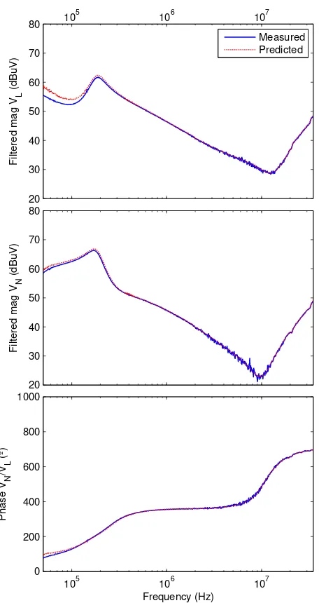
of the PLF (circuit S parameters) and the circuit characterization of the LISN (circuit S parameters) are used in figure 5.1 to simulate the interference propagation through the different devices. The simulated VL and VN voltage values have been compared with the conducted
emissions measured according to CISPR 22 [11], as seen in figure 5.3, in order to validate the prediction methodology. Figure 5.4 shows the comparison between the predicted and the measured conducted emissions. As can be seen, the prediction is practically superimposed on the measured values.
VL
VN
Line Load
PL PL
dev dev
mon mon
Figure 5.3: Block diagram for the measurement setup of the voltage in the line terminals of a DUT with a PLF.
Modal prediction
To perform a prediction of the modal conducted emissions of the test device, its modal characterization (ZCM, ZDM, ZT M, Vncm and Vndm, figure 3.3), the modal characterization
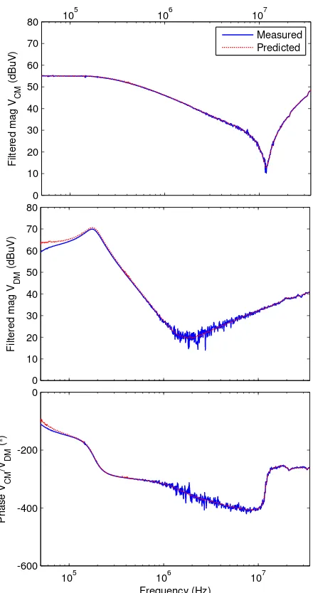
of the PLF (modal S parameters) and the modal characterization of the LISN (modal S pa-rameters) are used in figure 5.2 to simulate the interference propagation through the different devices. The simulated VCM and VDM voltage values have been compared with the modal
5.3 Experimental validation 71
105 106 107
20 30 40 50 60 70 80
Filtered mag V
L
(dBuV)
20 30 40 50 60 70 80
Filtered mag V
N
(dBuV)
105 106 107
0 200 400 600 800 1000
Frequency (Hz)
Phase V
N
/VL
(º)
[image:19.595.200.428.219.649.2]Measured Predicted
(1.1) on the measured VL and VN). Figure 5.5 shows the comparison between the predicted
and the measured modal emissions. As can be seen, the prediction is again superimposed on the measured values. The good agreement between the prediction and measurement validates both the proposed circuit and modal prediction methodologies.
105 106 107
0 10 20 30 40 50 60 70 80
Filtered mag V
CM
(dBuV)
0 10 20 30 40 50 60 70 80
Filtered mag V
DM
(dBuV)
105 106 107
0
-200
-400
-600
Frequency (Hz)
Phase V
CM
/V DM
(º)
[image:20.595.179.399.208.625.2]Measured Predicted
Figure 5.5: Predicted and measured circuit voltages (VCM andVDM) for the configuration of figure 5.3.
In order to state the importance of a complete modal characterization of the DUT, a prediction of the modal conducted emissions generated by the filtered DUT has been made, but this time with ZT M = ∞ to emulate a characterization of the DUT considering only its
5.3 Experimental validation 73
the DUT are not converted to the other mode by ZT M, as occurs in the actual device. Table
5.1 compares, at two selected frequencies, the measured levels of CM and DM interference at the line side of the PLF with the simulated ones with a DUT with ZT M = ∞. As can be
seen, the predicted values do not match the measured ones. This fact shows that in the design of an optimum PLF for a given DUT, its whole modal model has to be considered in order to account for all the modal conversions that can degrade its behavior. As can be seen in this example, not only the inner mode conversion at the components of the PLF can degrade its performance, but also the interactions (originated by mismatches) of the PLF with mode conversion mechanisms at the components of the DUT.
Voltages (dBuV) 176740 Hz 301155 Hz
MeasuredVCM 54.76 53.25
PredictedVCM without ZT M 52.36 50.11
Predicted VCM with ZT M 54.83 53.43
Measured VDM 69.89 55.94
Predicted VDM without ZT M 63.02 49.38
Predicted VDM withZT M 70.58 56.61
Table 5.1: Comparaison of the modal voltages (VCM,VDM) measured, predicted withZT M =∞and predicted
with theZT M of figure 3.19, for the test device of figure 3.7 and the PLF Belling-Lee SF4110-1.
Comparison with predictions using 50-Ω insertion loss characterization
As stated in chapter 1, insertion loss (IL) measurements in a 50-Ω measurement system are of little use when the PLF is connected to actual DUTs and PLNs. Besides, they do not detect the modal conversion between modes in the PLF. These facts lead to an unexpected decrease in the performance of the filter. It is, however, a common practice among EMC engineers to compute the expected values of conducted emissions of a DUT with a PLF simply by subtracting from the conducted emissions generated by the DUT (without the PLF) the values of the CM and DM attenuations of the PLF as measured by the standards. Figure 5.6 compares the predicted CM and DM voltages according to this common practice with the actual measured values. As can be seen, the error can be significant, in contrast to the results obtained using the method described in this chapter (figure 5.5). This fact corroborates the adequacy of the approach adopted in this chapter to predict conducted emissions.
5.3.2 Prediction of the conducted emissions of a real DUT
Circuit prediction
105 106 107 0
10 20 30 40 50 60 70 80
Frequency (Hz)
Filtered mag V
CM
(dBuV)
Measured Predicted with traditional method
105 106 107
0 20 40 60 80
Frequency (Hz)
Filtered mag V
DM
(dBuV)
Figure 5.6: Comparison between the conducted emissions predicted according to the common engineering practice and the measured ones.
emissions have been computed using the circuits of figures 5.1 and 5.2 respectively. Both circuits contain theS parameters of the PLF Konfektronic GMBH 2A. The actual emissions have also been measured using the setup of figure 5.3. Figure 5.7 compares the measured and predicted values of the magnitudes of VL and VN at the line side of the PLF. A set of interference in
the band from 150 kHz to 2 MHz, generated by the switching power supply of the transceiver, can be seen. Interference at multiple frequencies of 4 MHz are also noticeable. By simulating the effect of the PLF on the DUT, some frequencies have been attenuated to levels around -10 dBµV. However, interference levels below 10 dBµV cannot be compared due to the noise floor level of the measurement system (figure 5.3). Beyond 10 dBµV, a good agreement is obtained. The attenuation effect of the PLF is specially observed if the emissions are compared with the ones of figure 3.23.
106 107
-20 0 20 40 60 80
Frequency (Hz)
Filtered mag V
L
(dBuV)
Measured Predicted
106 107
-20 0 20 40 60 80
Frequency (Hz)
Filtered mag V
N
(dBuV)
5.3 Experimental validation 75
Modal Prediction
Figure 5.8 shows the comparison between the predicted and measuredVCM and VDM
volt-ages at the line side of the PLF. The very good agreement between the measurement and prediction validates the approach presented in this chapter, and shows that it is possible to predict the levels of conducted emissions that a generic DUT loaded with a PLF generates according to the desired standard (in this case, with the measurement setup of CISPR 16 [12]). This approach can be very useful in the design of an electronic device (or its PLF), since its levels of conducted emissions can be predicted easily when loaded with previously measured PLFs. This way, long and costly sessions of filter assembly and measurement can be avoided: the DUT has to be measured only once (in order to obtain its circuit and modal models), and its behavior when connected to a set of previously measured filters (as described in chapter 2) easily and rapidly predicted using the presented methodology.
106 107
-20 0 20 40 60 80
Frequency (Hz)
Filtered mag V
CM
(dBuV)
Measured Predicted
106 107
-20 0 20 40 60 80
Frequency (Hz)
Filtered mag V
DM
(dBuV)
Figure 5.8: Predicted and measured modal voltagesVCM andVDM for the 100-W HF transceiver.
Comparison with predictions using 50-Ω IL characterization
As in the previous example, the predictions made by the method described in this chapter have been compared to the predictions made using the PLF attenuations given by the IL in a 50-Ω measurement system. Figure 5.9 compares the modal voltagesVCM and VDM according
106 107 -20
0 20 40 60 80
Frequency (Hz)
Filtered mag V
CM
(dBuV)
Measured Predicted with traditional method
106 107
0 20 40 60 80
Frequency (Hz)
Filtered mag V
DM
(dBuV)
Chapter 6
Power-Line Filter Design from
S
-Parameter Measurements
Contents of this chapter
6.1 Introduction . . . 77
6.2 Methodology for a PLF design . . . 78
6.3 Experimental validation . . . 81
6.3.1 PLF design for a switching power supply with stationary noise . . . . 81 6.3.2 Filtering comparison with a different component position . . . 88 6.3.3 PLF design for a switching power supply with non-stationary noise . . 89
6.1
Introduction
The traditional power-line filter (PLF) design techniques reviewed in the introduction suf-fered from several disadvantages:
- Using the separated common-mode (CM) and differential-mode (DM) equivalent circuits of a general PLF, the methodologies presented in [49]–[53] find the suitable values of X capacitors, common-mode chokes (CMCs) and Y capacitors considering only their ideal behavior. This can lead to a wrong prediction of the PLF attenuation due to the non-ideal behavior at high frequencies and the mode conversion produced by asymmetric components.
Therefore, the development of a new PLF design technique that improves all these points is needed to implement better PLFs. This methodology has to consider the parasitic impedances and the mode conversion in CMC, X- and Y-capacitor networks, and their best position in the PLF to obtain optimal results.
Different techniques to characterize the parasitic capacitances, the leakage inductance or the actual impedance under in-circuit conditions of CMCs are presented in [29], [122]–[126], and the equivalent circuit of a real capacitor can be found in [127]. These techniques are useful to analyze the characteristics of the PLF components, but they do not present a complete solution from the modal point of view: either they do not contribute with modal information, or they separate the CM and DM attenuation without considering the mode conversion. As can be observed, a similar problem was faced in chapter 2 with the PLF characterization, and the scattering (S) parameters were successfully used in that case. Considering the PLF as a four-port device, the actual CM and DM attenuation and mode conversion appear explicitly in the modal S parameters. Therefore, if the individual components that constitutes the PLF can be analyzed as four-port networks, the same characterization can be applied.
In this chapter, a new PLF design methodology based on theS-parameter characterization is presented. This methodology uses the measured S parameters of each component to compute their combined responses, and finds the best PLF to mitigate the conducted emissions of a particular device under test (DUT) according to the requirements of the designer. For instance, the best PLF can be the one that introduces the maximum attenuation, or the one that presents the lowest cost. The structure followed in this chapter is as follows: the design methodology is presented in detail in the second section, and it is validated in the third section with the results obtained from measurements on real devices with both stationary and non-stationary emissions.
6.2
Methodology for a PLF design
The proposed methodology to design a PLF consists of the following steps:
1. Characterization of CMCs and X and Y capacitors. To this end, four-port networks composed by individual CMCs, X and Y capacitors have been implemented. The block diagram of each network is shown in figure 6.1, and the appearance of some actual im-plementations can be seen in figure 6.2. For an accurateS-parameter measurement, each port has been connected to a SMA connector, and the information of all the components is stored in a database for a later treatment.
2. Generation of PLFs from first to nth order by using the previous database. This
6.2 Methodology for a PLF design 79
M L1
L2
CMC network X-capacitor network CX Y-capacitor network CY1 CY2 L G N G L G N G L G N G L G N G
Figure 6.1: Block diagram of the implementation of CMC, X-capacitor and Y-capacitor networks.
Figure 6.2: CMCs and capacitors placed in individual boards.
6.3(a)). The PLFs of second order are obtained joining theS parameters of two networks in cascade (figure 6.3(b)). The PLFs ofnth order are obtained joining theS parameters
ofnnetworks in cascade (figure 6.3(c)).
Network 1
(a) PLF of order 1
Network 1
(b) PLF of order 2 Network
2
Network 1
(c) PLF of order n
Network 2 Network n L G N G L G N G L G N G L G N G L G N G L G N G
Figure 6.3: Block diagram of the PLF implementation: (a) PLF of order 1; (b) PLF of order 2; (c) PLF of ordern.
3. Characterization of the DUT as it was explained in chapter 3.
4. Characterization of the line impedance stabilization network (LISN) as it was explained in chapter 2. If the predicted conducted emissions levels in a real power-line network (PLN) are desired, the PLN can be characterized as it was explained in chapter 3.
mon
mon
dev
dev
VL
VN
ZL
VnL
ZT
ZN
VnN
1st
network 2nd
network
nth
[image:28.595.131.447.184.344.2]network
Figure 6.4: Block diagram for the simulation of the circuit conducted emissions of a DUT connected to a PLF ofnthorder.
M M M
CM
DM
CM
DM
VCM
VDM
VnCM
VnDM
ZCM
ZDM
ZTM
1st
network 2nd
network
nth
network
[image:28.595.132.448.518.668.2]6.3 Experimental validation 81
X-capacitor values [nF]
[image:29.595.213.407.139.169.2]10 15 22 33 47 68 100 220
Table 6.1: Measured X-capacitor networks for the PLF design methodology.
Y-capacitor values [nF] 1.5 2.2 3.3 4.7 6.8 10
Table 6.2: Measured Y-capacitor networks for the PLF design methodology.
[image:29.595.211.413.370.437.2]6. Once the optimal PLF is obtained by computation, it can be implemented by joining its actual components. Figure 6.6 shows an example of a PLF composed by a X-capacitor, a CMC and a Y-capacitor network.
Figure 6.6: Connection of three different components to build a complete PLF.
6.3
Experimental validation
6.3.1 PLF design for a switching power supply with stationary noise This section analyzes in detail each step of the PLF design methodology.
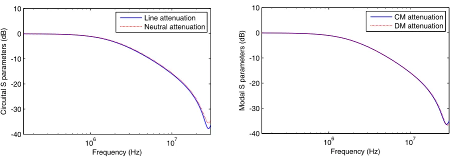
1. TheS parameters of several networks composed by X capacitors (one capacitor per net, with the values shown in table 6.1), Y capacitors (two capacitors per net, with the values shown in table 6.2), and CMCs (one CMC per net, with the values shown in table 6.3) have been measured. Figures 6.7, 6.8 and 6.9 show the circuit and modalSparameters of three examples: a network composed by a X capacitor of 100 nF (which only affects the DM), a network composed by two Y capacitors of 3.3 nF (which affects both the CM and DM beyond 1 MHz) and a network composed by a CMC of 10 mH (which mainly affects the CM, but there is also an attenuation on the DM due to the leakage flux) respectively.
CMC values [mH] 1 2.2 3.3 5 10 20
Table 6.3: Measured CMC networks for the PLF design methodology.
106 107
-10 -8 -6 -4 -2 0
Frequency (Hz)
Circuital S parameters (dB)
106 107
-60 -50 -40 -30 -20 -10 0 10 20
Frequency (Hz)
Modal S parameters (dB)
Line attenuation Neutral attenuation
[image:30.595.69.517.301.456.2]CM attenuation DM attenuation
Figure 6.7: Circuit and modalS parameters of a network composed by a X capacitor of 100 nF.
106 107
-40 -30 -20 -10 0 10
Frequency (Hz)
Circuital S parameters (dB)
106 107
-40 -30 -20 -10 0 10
Frequency (Hz)
Modal S parameters (dB)
Line attenuation Neutral attenuation
[image:30.595.66.516.554.711.2]CM attenuation DM attenuation
6.3 Experimental validation 83
106 107
-50 -40 -30 -20 -10 0 Frequency (Hz)
Circuital S parameters (dB)
106 107
-60 -50 -40 -30 -20 -10 0 10 20 Frequency (Hz)
Modal S parameters (dB)
Line attenuation Neutral attenuation
[image:31.595.89.534.122.283.2]CM attenuation DM attenuation
Figure 6.9: Circuit and modalS parameters of a network composed by a CMC of 10 mH.
Y-capacitor and CMC networks shown separately before. The combined effect of the three components present an strong attenuation on both CM and DM.
106 107
-80 -70 -60 -50 -40 -30 -20 -10 Frequency (Hz)
Circuital S parameters (dB)
106 107
-80 -70 -60 -50 -40 -30 -20 -10 0 Frequency (Hz)
Modal S parameters (dB)
Line attenuation Neutral attenuation
CM attenuation DM attenuation
Figure 6.10: Circuit and modalSparameters of a PLF composed by a X capacitor of 100 nF, two Y capacitors of 3.3 nF and a CMC of 10 mH.
3. The DUT characterized and used for the validation is a switching power supply that feeds a microcontroller with a 4 MHz clock (figure 6.11). Figure 6.12 shows its circuit conducted emissionsVLandVN measured according to [11]. As can be seen, the conducted emissions
exceed the quasi-peak limit for class B devices established in [11].
The modal conducted emissions VCM and VDM have been computed using (1.1) and
compared with the circuit limit in figure 6.13 for guidance only (since there is no limit for the modal conducted emissions). Both modal components contain the 4-MHz clock and exceed the circuit limit in a wide frequency range.
[image:31.595.91.540.381.536.2]Figure 6.11: Microcontroller with a 4 MHz clock used to validate the PLF design methodology.
106 107
10 20 30 40 50 60 70 80 90 Frequency (Hz) Mag V L (dBuV)
106 107
[image:32.595.72.517.335.494.2]10 20 30 40 50 60 70 80 90 Frequency (Hz) Mag V N (dBuV) Mag V L Límit Mag V N Límit
Figure 6.12: Circuit conducted emissionsVLandVN of the switching power supply without any PLF.
106 107
10 20 30 40 50 60 70 80 90 Frequency (Hz) Mag V CM (dBuV)
106 107
10 20 30 40 50 60 70 80 90 Frequency (Hz) Mag V DM (dBuV) Mag V DM Limit Mag V CM Limit
[image:32.595.70.518.566.725.2]6.3 Experimental validation 85
106 107
-20 -15 -10 -5 0
Frequency (Hz)
Circuital S parameters (dB)
106 107
-20 -15 -10 -5 0
Frequency (Hz)
Modal S parameters (dB)
CM atteunation DM attenuation Line attenuation
[image:33.595.89.534.121.283.2]Neutral attenuation
Figure 6.14: Circuit and modalSparameters of the LISN.
5. The predictions of the conducted emissions of the switching power supply with all the PLFs generated in step 2 are realized. Figure 6.15 shows the circuit conducted emissions of the DUT connected to a first-order PLF composed by a CMC of 10 mH. As can be seen, this PLF does not mitigate the conducted emissions under the circuit limit and it can be discarded as a possible PLF. On the other hand, figure 6.16 shows the circuit conducted emissions of the DUT connected to a third-order PLF composed by a X capacitor of 100 nF, two Y capacitors of 3.3 nF and a CMC of 10 mH. This is one of the possible PLFs since it attenuates the interference levels of the DUT under the limit.
106 107
10 20 30 40 50 60 70 80 90
Frequency (Hz)
Mag V
L
(dBuV)
106 107
10 20 30 40 50 60 70 80 90
Frequency (Hz)
Mag V
N
(dBuV)
Figure 6.15: Circuit conducted emissionsVL and VN of the switching power supply with a first-order PLF composed by a CMC of 10 mH.
[image:33.595.91.539.480.634.2]106 107 10
20 30 40 50 60 70 80 90
Frequency (Hz)
Mag V
L
(dBuV)
106 107
10 20 30 40 50 60 70 80 90
Frequency (Hz)
Mag V
N
[image:34.595.70.516.110.282.2](dBuV)
Figure 6.16: Circuit conducted emissions VLand VN of the switching power supply with a third-order PLF composed by a X capacitor of 100 nF, two Y capacitors of 3.3 nF and a CMC of 10 mH.
by a CMC of 20 mH and a X capacitor of 100 nF, as seen in figure 6.17. As the PLF of figure 6.16, this one attenuates the interference levels under the limit. However, it does not need the Y-capacitor network and, therefore, is cheaper.
100 nF X C = 1 20 mH
L=
DUT L
N G LISN
2 20 mH L =
M
PLF
Line side Load side
Ldev
Ndev
[image:34.595.145.434.407.530.2]G
Figure 6.17: Structure of the optimal PLF obtained with the design methodology.
6. The optimal PLF obtained in step 5 has been implemented and connected to the DUT. Figure 6.18 shows the predicted and measured circuit conducted emissions of the set DUT plus PLF. The good agreement between them corroborates that it is possible to design the PLF from the S-parameter measurements of its individual components and reduce the conducted emissions under the limit with a PLF optimized in terms of cost.
6.3 Experimental validation 87
106 107
10 20 30 40 50 60 70 80 90 Frequency (Hz) Mag V L (dBuV)
106 107
10 20 30 40 50 60 70 80 90 Frequency (Hz) Mag V N (dBuV)
[image:35.595.90.538.130.313.2]Mesured Predicted Limit
Figure 6.18: Circuit conducted emissionsVLandVN of the switching power supply with a PLF composed by a CMC of 20 mH and a X capacitor of 100 nF.
is still decreasing its impedance inversely proportional to the frequency and increasing its attenuation on the DM.
106 107
10 20 30 40 50 60 70 80 90 Frequency (Hz) Mag V CM (dBuV)
106 107
10 20 30 40 50 60 70 80 90 Frequency (Hz) Mag V DM (dBuV)
Measured Predicted Limit
Figure 6.19: Modal conducted emissionsVCM andVDM of the switching power supply with a PLF composed by a CMC of 20 mH and a X capacitor of 100 nF.
[image:35.595.89.540.416.601.2]6.3.2 Filtering comparison with a different component position
The position of the different components in the PLF is not trivial, since different positions can lead to important variations of the conducted emission levels. To show this effect, the PLF of figure 6.17 has been modified by swapping the two components, as seen in figure 6.20. Figure 6.21 compares the circuit conducted emissions measured with the two PLF configurations. As can be seen, both PLF, that are composed by the same components but in a different position, present different attenuations on the conducted emissions of the switching power supply. With the swapped filter the emissions at the frequency of 170 kHz are over the limit, and at the frequency of 650 kHz there is a difference of about 30 dB with regard to the first PLF. Therefore, the methodology presented to design the PLF by computing all possible configurations improves those techniques based on fixed PLF structures [49]–[53], [57], [58].
LISN
100 nF X
C = L1=20 mH
DUT L
N G
2 20 mH L =
M PLF
Line side Load side
Ldev
Ndev
[image:36.595.147.434.335.457.2]G
Figure 6.20: Structure of the swapped PLF.
106 107
10 20 30 40 50 60 70 80 90
Frequency (Hz)
Mag V
L
(dBuV)
106 107
10 20 30 40 50 60 70 80 90
Frequency (Hz)
Mag V
N
(dBuV)
Measured with the swaped PLF Measured with the original PLF Limit
[image:36.595.67.521.515.720.2]6.3 Experimental validation 89
6.3.3 PLF design for a switching power supply with non-stationary noise The same methodology can be applied to the switching power supply of chapter 4, which conducted emissions, measured in time domain, were characterized by the presence of impulsive noise (figure 4.11). Figure 6.22 shows the circuit and modal conducted emissions of the switch-ing power supply compared with the quasi-peak limit for class B devices established in [11]. As can be seen, the circuit conducted emissions are over the limit and they are mainly dominated by the DM, which means that the PLF has to be designed to mitigate this mode. The PLF obtained after applying the design methodology is shown in figure 6.23, and, as expected, it is exclusively composed by a X capacitor of 100 nF.
106 107
10 20 30 40 50 60 70 80 90
Frequency (Hz)
Circuital emissions (dBuV)
106 107
10 20 30 40 50 60 70 80 90
Frequency (Hz)
Modal emissions (dBuV)
L emissions N emissions Limit
[image:37.595.92.538.294.447.2]CM emissions DM emissions Limit
Figure 6.22: Circuit and modal conducted emissions of the switching power supply with non-stationary noise.
LISN
100 nF X C =
DUT L
N G PLF
Line side Load side
Ldev
Ndev
[image:37.595.167.455.510.635.2]G
Figure 6.23: Structure of the PLF designed by the methodology.
Figure 6.24 shows the comparison between the predicted and measured circuit conducted emissions of the switching power supply connected to the PLF of figure 6.23. As can be seen, the predicted emissions are similar to the measured ones, which proves that it is possible to design a suitable PLF for a DUT with impulsive emissions using the methodology proposed in this chapter.
106 107 10 20 30 40 50 60 70 80 90 Frequency (Hz) Mag V L (dBuV)
106 107
[image:38.595.69.519.129.287.2]10 20 30 40 50 60 70 80 90 Frequency (Hz) Mag V N (dBuV) Predicted Measured Class B Limit
Figure 6.24: Comparison between the predicted and measured circuit conducted emissions of the switching power supply connected to the PLF of figure 6.23.
supply connected to the PLF of figure 6.23 (the circuit limit has also been plotted for guidance). The CM emissions are similar to the ones of figure 6.22, since a X capacitor placed between L and N terminals does not affect this mode, but the DM emissions are considerably reduced. Even though the DM is over the limit for class B devices under 200 kHz, the circuit values (VL
and VN) which are composed by the combination of this mode with the CM, are under the
limit.
106 107
10 20 30 40 50 60 70 80 90 Frequency (Hz) Mag V CM (dBuV)
106 107
10 20 30 40 50 60 70 80 90 Frequency (Hz) Mag V DM (dBuV)
[image:38.595.68.518.457.611.2]Chapter 7
Power-Line Filter Design Using
Mode Conversion
Contents of this chapter
7.1 Introduction . . . 92
7.2 Modal characterization of PLF capacitors . . . 93
7.2.1 Characterization of a shunt-connected two-port network . . . 93 7.2.2 X capacitor network . . . 95 7.2.3 Y capacitors network . . . 95 7.2.4 Star Capacitor Network . . . 96 7.3 Modal characterization of CMCs . . . 96
7.3.1 Characterization of a series-connected two-port network . . . 96 7.3.2 CMC network . . . 98 7.4 Parametric study of the mode conversion . . . 99
7.4.1 Simulations with ideal capacitors . . . 99 7.4.2 Simulations with ideal CMCs . . . 100 7.5 Design of the optimal components of a PLF . . . 102
7.5.1 Performance of the genetic algorithm . . . 102 7.5.2 Example with an actual DUT . . . 103 7.6 Experimental Validation . . . 105
PLF design using the mode conversion in a CMC . . . 110
7.1
Introduction
The methodology of the previous chapter was useful to design power-line filters (PLFs) using the classical symmetric structure, that is, an structure that avoids mode conversion. This structure has been proven to be efficient for the common-mode (CM) and differential-mode (DM) filtering, and the efforts to optimize the effect of a PLF are usually performed preserving this symmetry. For instance, the use of nanocrystalline material for the common-mode choke (CMC) core is proposed in [134] because of the good relationship between permeability and saturation. A model that predicts and optimizes the leakage flux in the core to increase the DM attenuation in a CMC by choosing the appropriate core material is presented in [122], and the use of a magnetically permeable bypass for the same purpose is suggested in [135].
However, a different point of view to optimize the PLF capabilities is arisen in this chapter: instead of using the classical symmetric structure, asymmetries are introduced in the circuit to produce mode conversion. Mode conversion is an energy exchange between CM and DM, and the objective is to determine whether this conversion can be used, for instance, to reduce the dominant mode of a conducted-emissions problem using fewer or smaller components than in a symmetric PLF. This point of view applied on the design of PLFs is completely novel since no previous references about this particular topic have been found in the literature.
7.2 Modal characterization of PLF capacitors 93
filtering of its PLF.
7.2
Modal characterization of PLF capacitors
7.2.1 Characterization of a shunt-connected two-port network
A generic two-port network shunt-connected to the line (L), neutral (N) and ground (G) terminals can be seen in figure 7.1 (G is the ground of the measurement system) [136]. The voltages and currents at the terminal ports of the network are VIL = VOL, VIN = VON, IIL=−IOL andIIN =−ION. The two-port network can be mathematically characterized, for
instance, by itsZ parameters:
V1 = Z11I1+Z12I2
V2 = Z21I1+Z22I2
(7.1) L L G G N N + -Two-port network + -1 IL OL
V =V =V
IL I OL I IN I ON I
2 IN ON
V =V =V
1
[image:41.595.201.421.323.534.2]I I2
Figure 7.1: Impedance network connected to L, N and G terminals.
Using (7.1) and analyzing the circuit of figure 7.1, the equations that completely characterize its behavior are obtained:
VIL =VOL = Z11(IIL+IOL) +Z12(IIN +ION) VIN =VON = Z21(IIL+IOL) +Z22(IIN +ION)
(7.2)
Combining (1.1) and (7.2), the equations that characterize the modal behavior of the impedance network of figure 7.1 can be obtained as:
VID √ 2 = IIC √ 2 + IOC √ 2
Z11−Z22 2
+√2IID+
√
2IOD
Z11+Z22−2Z12
2
√
2VIC =
IIC √ 2 + IOC √ 2
Z11+Z22+ 2Z12 2
+√2IID+
√
2IOD
Z
11−Z22 2
A modal model for the generic circuit of figure 7.1 has to split each mode into a different port and its behavior has to be described by (7.3). This model can be obtained by a generalization of the modal model for asymmetric shunt impedances presented in [137], and it is shown in figure 7.2. It is composed by two equal impedance networks with their terminals connected between the CM and DM paths, and splits the contribution of each mode into a different port (namely, input CM into port 1, input DM into port 2, output CM into port 3 and output DM into port 4). Its structure allows a simple interpretation of the modal energy propagation: an interaction between CM and DM can exist, and this interaction is determined by the two impedance networks that connect the CM path to the DM path.
1 : 2
1 : 2
+ -+ -2 ID V 2 ID I + -2 OD V
2IOD
2VIC
2 IC
I
+
-2VOC
2 OC I + -+ -+ -Por
t 2 +
-+ -+ -Po rt 1 Por t 4 P or t 3 IC I OCM Z IC a IC b IC V
2 : 1 ID I ODM Z ID a ID b ID V 1 V 2 V + -+ -2 V 1 V
2 : 1 OC
I OCM Z OC a OC b OC V OD I OCM Z OD a OD b OD V Two-port network Two-port network
Figure 7.2: Modal model of a shunt-connected two-port network.
By analyzing the modal model of figure 7.2, its modalS-parameter matrix can be obtained as: bIC bID bOC bOD = 1 ∆ α β χ β β δ β χ χ β α β β χ β δ aIC aID aOC aOD (7.4) where
α=−4Z0CM(Z11+Z22−2Z12)−2Z0CMZ0DM β = 2√Z0CMZ0DM(Z11−Z22)
χ= 8Z11Z22−8Z122 +Z0DM(Z11+Z22+ 2Z12)
δ =−Z0DM(Z11+Z22+ 2Z12)−2Z0CMZ0DM
∆ = 8Z11Z22−8Z122 + 4Z0CM(Z11+Z22−2Z12) + +Z0DM(Z11+Z22+ 2Z12) + 2Z0CMZ0DM
7.2 Modal characterization of PLF capacitors 95
The reference impedance for the CM (port 1 and port 3) is Z0CM and the reference
impedance for the DM (port 2 and port 4) is Z0DM. From the S-parameter matrix it can
be concluded that mode conversion from CM to DM and vice versa is produced by the param-eterβ/∆. IfZ11 is different fromZ22, mode conversion will take place in the circuit.
The generic model of figure 7.1 can be adapted, among others, to the capacitor impedance networks commonly found in a PLF, such as X capacitor networks and Y capacitors networks, or to less used capacitor impedance network topologies such as an star capacitor network. Therefore, their respective modal models can be found with the modal model of figure 7.2.
7.2.2 X capacitor network
A X capacitor network is composed by a X capacitor placed between the L and N terminals with an impedance ZCX, as can be seen in figure 7.3(a). The modal model of this network
is shown in figure 7.3(b), and can be further simplified into the circuit of figure 7.3(c). As expected, a network composed by a X capacitor between L and N terminals has influence only on the DM. The CM remains unaffected by the X capacitor.
2 :1 2 :1 1: 2 + -+ -+ -+ -+ -+ -+ -+ -(b) (c) Port 2 Port 1 Po rt 4 P ort 3 Port 2 Port 1 Port 4 P ort 3 L L G G N N + -+ -(a) IL I OL I CX Z IN I ON I IL OL
V =V VIN =VON ZCX ZCX
CX Z 1: 2 ID I ID V IC I IC V ID I ID V IC I IC V OD I OD V OC I OC V OD I OD V OC I OC V
Figure 7.3: Models for X capacitor networks: (a) Circuit model. (b) Full modal model. (c) Simplified modal model.
7.2.3 Y capacitors network
2 :1 2 :1 1: 2 1: 2 + -+ -+ -+ -Port 2 Port 1 Port 4 P ort 3 L L G G N N + -+ -(a) (b) IL I OL I 1 C Y Z IN I ON I IL OL
V =V VIN =VON
2 CY Z ID I ID V IC I IC V OD I OD V OC I OC V 1 CY Z 2 CY Z 2 CY Z 1 CY Z
Figure 7.4: Models for Y capacitor networks: (a) Circuit model. (b) Modal model.
7.2.4 Star Capacitor Network
Although PLFs are usually composed by the X and Y capacitor topologies, the generic model of figure 7.2 can also be applied to less frequent topologies such as the star capacitor network, as seen in figure 7.5(a). Its equivalent modal model can be seen in figure 7.5(b). As can be expected, if ZC3 → 0 the modal model for Y capacitors is recovered, whereas if
ZC3 → ∞ the modal model for X-class capacitors is obtained.
2 :1 2 :1 1: 2 1: 2 + -+ -+ -+ -Port 2 Po rt 1 Port 4 P ort 3 L L G G N N + -+ -(a) (b) IL I OL I IN I ON I IL OL
V =V
3 C Z ID I ID V IC I IC V OD I OD V OC I OC V 1 C Z IN ON
V =V
1 C
Z ZC2 ZC2
2 C
Z ZC1
3 C
Z ZC3
Figure 7.5: Models for star capacitor networks: (a) Circuit model. (b) Modal model.
7.3
Modal characterization of CMCs
7.3.1 Characterization of a series-connected two-port network
A similar procedure can be applied to a generic two-port network series-connected to the L and N terminals, as seen in figure 7.6 [138]. The voltages and currents in the terminals of this network are VIL=VOL,VIN =VON,IIL =−IOL and IIN =−ION. This network can be
7.3 Modal characterization of CMCs 97 Two-port network L + -IL I 1
I V1 1
I
+V2 -2
I I2
G N L’ G’ N’ OL I IN
I ION
+ -IL V + -OL V + -IN V + -IN V
Figure 7.6: Two-port network series-connected to the L and N terminals.
Analyzing the circuit of figure 7.6 and using (7.1), the following equations are obtained:
VIL−VOL = Z11IIL+Z12IIN VIN−VON = Z21IIL+Z22IIN
(7.6)
Combining (1.1) and (7.6), the equations that characterize the modal behavior of the circuit of figure 7.6 are found:
VID √ 2 − VOD √ 2 = IIC √ 2
Z11−Z22 2
+√2IID
Z11+Z22−2Z12 2
√
2VIC−
√
2VOC = IIC
√
2
Z11+Z22+ 2Z12 2
+√2IID
Z11−Z22 2
(7.7)
A modal model for the generic circuit of figure 7.6, which splits each mode into a different port, has to be described by (7.7). This model can be obtained as a generalization of the modal model for asymmetric series-impedances presented in [139], and it is shown in figure 7.7. This structure allows a simple interpretation of the modal propagation: in particular, an interaction between CM and DM can exist through the two-port networks that connect the CM path to the DM path. As can be seen, this connection is different from the one present in the modal model of figure 7.2.
By analyzing the modal model of figure 7.7, its modalS-parameter matrix can be obtained:
+ -+ -Xarxes de dos ports + -+ -+ -+ -+ -+ -+ -+ -+ -+ -P o rt 1 P or t 2 Po rt 4 P o rt 3
2 : 1
2 : 1 1 : 2
2 ID V 2 ID I 2 OD V
2IOD
2 IC V 2 IC I 2 OC V 2 OC I OD I OD V 0DM Z OD a OD b OC I OC V 0CM Z OC a OC b IC I IC V IC a IC b 0CM Z ID I ID V ID a ID b 0DM Z 1 V 2 V 2 V 1 V
1 : 2
Two-port network
Two-port network
Figure 7.7: Modal model of a series-connected two-port network.
where
α= 2Z11Z22−2Z122 +Z0DM(Z11+Z22+ 2Z12),
β = 2√Z0CMZ0DM(Z11−Z22),
χ= 4Z0CM(Z11+Z22−2Z12) + 8Z0CMZ0DM, δ = 2Z11Z22−2Z122 + 4Z0CM(Z11+Z22−2Z12),
ε=Z0DM(Z11+Z22+ 2Z12) + 8Z0CMZ0DM,
∆ = 2Z11Z22−2Z122 + 4Z0CM(Z11+Z22−2Z12) + +Z0DM(Z11+Z22+ 2Z12) + 8Z0CMZ0DM
(7.9)
As before, Z0CM is the reference impedance for the CM (ports 1 and 3), and Z0DM is
the reference impedance for the DM (ports 2 and 4). From the S-parameter matrix it can be concluded that the mode conversion from CM to DM and vice versa is controlled by β/∆. Whenever Z11 and Z22 are different, mode conversion takes place.
7.3.2 CMC network
7.4 Parametric study of the mode conversion 99 2 :1 2 :1 1: 2 + -+ -+ -+ -(b) Port 2 Port 1 Port 4 P ort 3 L L G G N N + -+ (a) IL I OL I IN I ON I IL
V VIN
1: 2 ID I ID V IC I IC V OD I OD V OC I OC V M M 1
L L2
2
L L1
ON V OL V M + 1
L L2
+
-Figure 7.8: Ideal CMC series-connected to the L and N terminals (a) and its modal model (b).
7.4
Parametric study of the mode conversion
The mode conversion in a PLF can be expressly provoked by the addition of asymmetries in its Y capacitors (CY1 6= CY2) or in its CMC (L1 6= L2), and used to improve its filtering capabilities. To show this effect, the conducted emissions of a test device connected to a PLF composed by capacitors first, and by a CMC later, have been simulated in order to compare their symmetrized and asymmetrized responses.
7.4.1 Simulations with ideal capacitors
To perform the study of the mode conversion in a PLF composed by ideal capacitor net-works, the modal model of a generic DUT has been connected to the modal model of two ideal Y-class capacitors (figure 7.4(b)) and to the simplified modal model of an ideal X-class capacitor of CX = 22 nF (figure 7.3(c)). Finally, the capacitors are connected to the modal
model of a passive PLN (the interference in the PLN is not considered for simplicity). The particular values for the modal models of the DUT and the PLN used in the simulations are shown in Table 7.1.
Table 7.1: Modal model values of the DUT and the PLN.
Component DUT PLN
ZCM [Ω] 25.3 + j5.6 20 + j0.6 ZDM [Ω] 160.2 - j18.3 35 + j3.3 ZT M [Ω] 50.7 + j32.1 130 + j62.1 VnCM [dBµV] 95.58
-VnDM [dBµV] 87.31
2 :1
2 :1
1 : 2
(a) (b) (c)
1: 2 1 Y C 1 Y C 2 Y C 2 Y C nDM V nCM V TM Z DM Z CM Z TM Z DM Z CM Z X
C VDMout
CMout V
DUT Ideal Y and X capacitors PLN
Figure 7.9: Propagation of the modal interference in the modal model of Y and X capacitors (b), placed between the modal model of a DUT (a) and the modal model of a PLN without interference (c).
of CY1. As can be seen, asymmetrizing the values of CY1 from 10 nF to 1.8 nF produces a slight reduction of the attenuation of the CM, and a significant increase of the attenuation of the DM (up to 25 dB average at high frequencies). Therefore, non-standard configurations of Y capacitors can give interesting results, such as this significant reduction of VDM out at
the expense of a small increment of VCM out (this increase can be tolerable or not depending
on the rest of the filter components). In general, for balanced DUTs and PLNs, balanced values of Y-capacitor networks yield the best mitigation, but for unbalanced DUTs and PLNs, asymmetrized Y-capacitor networks improve the filter performance.
106 107
20 30 40 50 60 70 80 90 100 Frequency (Hz) VCMout (dBuV)
CY1 = 10 nF C
Y1 = 3 nF
C
Y1 = 1,8 nF
106 107
20 30 40 50 60 70 80 90 100 Frequency (Hz) VDMout (dBuV)
Figure 7.10: VCM out andVDM outfor different values ofCY1.
7.4.2 Simulations with ideal CMCs
7.4 Parametric study of the mode conversion 101
modal model of a DUT and the modal model of a passive PLN. The parametric investigation has been performed considering several DUTs, PLNs, and CMCs, modeled by their respective modal models. As an example consider the DUT and the PLN whose modal parameters are shown in Table 7.2.
2 :1
2 :1
1: 2
(a) (b) (c)
1: 2 nDM
V
nCM
V
TM
Z
DM
Z
CM
Z
TM
Z
DM
Z
CM
Z
DMout
V
CMout
V
M M
1
L
2
L
2
L L1
DUT Ideal CMC PLN
Figure 7.11: Propagation of the modal interference in the modal model of CMCs (b), placed between the modal model of a DUT (a) and the modal model of a PLN without interference (c).
Table 7.2: Modal model values of the DUT and the PLN.
Component DUT PLN
ZCM [Ω] 3607 + j366 20 + j0.6
ZDM [Ω] 3 - j4 35 + j3.3
ZT M [Ω] 4502-j2151 130 + j62.1 VnCM [dBµV] 95.58
-VnDM [dBµV] 87.31
-Figure 7.12 shows VCM out and VDM out for different values of L2 while keeping the value of L1 to 20 mH. Unbalancing the values of L2 from 20 mH to 13 mH produces a significant decrease of both CM and DM (an average of 25 dB for the CM and 15 dB for the DM).
Therefore, non-standard configurations of CMCs can also achieve, in some cases, significant reductions ofVCM out and VDM out. From the performed parametric study, it can be concluded
106 107 40
50 60 70 80 90
Frequency (Hz)
V CMout
(dBuV)
106 107
40 50 60 70 80 90
Frequency (Hz)
VDMout
(dBuV)
L
2 = 20 mH
L
2 = 16.5 mH
L
2 = 13 mH
Figure 7.12: VCM out andVDM outfor different values ofL2.
7.5
Design of the optimal components of a PLF
It has been shown that it is possible to improve the performance of a PLF generating mode conversion in networks composed by Y capacitors and CMCs. Therefore, a PLF design tool should consider simultaneously the DUT’s conducted emissions, the DUT’s and PLN’s impedances, and all possible values of X capacitors, CMCs and Y capacitors that, with or without mode conversion, compose the optimal PLF, as for instance, regarding to cost. Be-cause of the great amount of variables, the design becomes impossible without an optimization technique. In order to deal with this problem, a GA has been developed to work as a PLF design tool. A GA is a searching procedure based on the mechanics of natural selection and genetics, and its features allow its use as an optimization technique for the PLF design problem [140]–[142].
7.5.1 Performance of the genetic algorithm