of Highly Ordered Organic Thin Films
of Phthalocyanine and Diindenoperylene
J. Oriol Ossó
En els darrers anys, materials orgànics amb propietats semiconductores han despertat molt interès. Aquests nous materials ofereixen molts avantatges da-vant els seus equivalents inorgànics com ara baix cost, flexibilitat i la possibilitat d’escollir d’entre un nombre quasi infinit de compostos diferents aquell que conté les propietats que ens interessen. A més, les anomenades molècules lleugeres, presenten propietats òptiques i electròniques molt interessants, que les fan ideals per a diverses aplicacions com ara dispositius transparents, guies d’ona i pantalles planes de grans dimensions. Actualment ja es comercialitzen diversos disposi-tius fabricats a partir de materials orgànics com ara pantalles de telèfons mòbils o de càmeres digitals. Similarment al cas dels semiconductors inorgànics conven-cionals, per a obtenir dispositius amb bones propietats electròniques es requereix l’obtenció del material en forma de capes primes amb un elevat ordre estructural i lliure d’impureses. Aquest aspecte és un problema en materials orgànics rela-cionat amb el caràcter feble de les forces d’interacció entre molècules (de ti-pus van der Waals). A més, la baixa simetria que presenten tan les molècules com les cel.les unitat dels cristalls que formen fan encara més difícil l’obten-ció de capes primes ben ordenades. A tot això sovint s’ha d’afegir el problema de polimorfisme, comú en molts d’aquests compostos. Les propietats òptiques i electròniques que les capes presenten depenen en gran mesura de l’estructura cristal.lina que aquestes adopten, determinada en part per les condicions en què la capa ha estat dipositada. Així, tot i que diversos dispositius basats en capes primes de molècules orgàniques ja han estat construïts (com díodes emissors de llum o OLEDs i transistors d’efecte camp o OFETs), s’ha fet evident que, com en el cas dels semiconductors tradicionals inorgànics, l’ordre cristal.lí del material que forma el dispositiu és clau per a obtenir el màxim rendiment de la capa activa orgànica.
En aquest treball, capes primes de materials orgànics han estat evaporades mit-jançant la tècnica d’epitàxia de feixos moleculars orgànics (OMBE). Les capes han estat dipositades sobre tipus diferents de substrats i sota condicions de creix-ement diverses, per a estudiar en quines condicions s’obté un grau d’ordre estruc-tural elevat. Els compostos orgànics utilitzats són coure-hexadecafluoroftalocianina (F16CuPc), semiconductor orgànic de tipusn, i diindenoperylene (DIP), de tipusp. Com a substrats s’han utilitzat tres òxids diferents, SiO2, MgO i Al2O3. S’ha re-alitzat un estudi sistemàtic de la influència de les condicions durant l’evaporació
que les capes presenten.
Per a estudiar les propietats estructurals de les capes s’han utilitzat princi-palment dues tècniques d’anàlisi, el microscopi de forces atòmiques (AFM) i la difracció de raigs-x. L’AFM és una tècnica que permet l’estudi de la morfologia del substrat i de la capa, i aporta informació sobre l’estructura en el pla de la capa. També resulta útil per a determinar la forma i les dimensions que els cristallets adopten i, a diferència de les tècniques de difracció, ens dona informació en l’es-pai real. La difracció de raigs-x ens ofereix informació no només sobre la super-fície sinó també sobre tot el volum de la capa i ens ajuda a caracteritzar l’estruc-tura tan en la direcció normal (reflectivitat de raigs-x) a la superfície com en el pla (difracció en incidència rasant). Les propietats òptiques es determinen util-itzant l’el.lipsometria espectral. Aquesta tècnica ha resultat particularment útil en l’anàlisi de l’anisotropia que algunes capes presenten. Tot i que l’estudi de materi-als amb propietats anisòtropes és complicat, l’el.lipsometria ens permet localitzar l’orientació del tensor dielèctric amb facilitat i quantificar el grau d’anisotropia de les capes orgàniques. Finalment, la tècnica d’espectroscòpia Raman s’ha utilitzat per a determinar el grau d’ordre i l’orientació de les molècules en la capa.
En aquest treball també s’ha estudiat la interfície entre materials orgànics, especialment les propietats estructurals a la interfície. Aquesta interfície és de rellevant importància ja que es necessària per a construir dispositius com cel.les solars orgàniques o díodes emissors de llum, on es requereixen capes orgàniques de diferents materials.
of Highly Ordered Organic Thin Films
of Phthalocyanine and Diindenoperylene
J. Oriol Ossó
Semiconducting organic materials have attracted interest during the last de-cades due to their interesting optoelectronic properties. Their application in new flexible and transparent devices, their tuning possibilities, and a potential low cost in the manufacturing lead to an increase of the academic activity in this field. The advances in the last decade attracted also the interest of the industry, and many companies have nowadays their own development division working on the field of organic electronics.
At present, many applications of organic semiconductors have been demon-strated, and several devices that use organic semiconducting materials can already be found in the market. In particular, low-weight organic molecules show very interesting optoelectronic properties for the development of new applications as transparent devices, waveguides, large-area flat displays, or organic solar cells. Similarly to the conventional inorganic semiconductors, in order to improve the electronic properties of the material highly ordered structures free of contaminants are required in the form of thin films.
However, the growth of organic thin films presents several problems inherently related to the nature of these relatively large molecules and the intermolecular van-der Waals forces between them. First of all, the unit cells of these materials are large compared to those of the typical inorganic substrates, and they exhibit a very low symmetry. Moreover, polymorphism is favored by the weak intermolecular interactions responsible of the crystal packing. The structural definition of the layers will determine their final optical and electronic properties. Due to these deviations from ideal growth, the physical properties of the organic layers do not hold compare to their single-crystal counterparts, which can be considered as the upper limit for some technologically relevant properties such as the charge carrier mobility.
Most of the studies on organic semiconducting materials deal only withp−type semiconductors (good hole conducting materials) since n-type and stable organ-ic semorgan-iconductors are rare. However, n−type materials are also needed in the construction of pn−junctions, as in solar cells, and also to implement the well-established complementary logic in organic circuits. In this work we study two or-ganic materials, ann-type compound of the family of the phthalocyanines and ap -type compound, diindenoperylene. Both of them are planar low-weight molecules.
study the influence of those parameters on the properties of the layers. We deter-mine under which deposition conditions the structure of the layers is optimized and which is the influence that the different substrates have on the final structure. We have studied two different organic compounds, copper-hexadecafluorophthalo-cyanine (F16CuPc), which is an n-type semiconductor, and diindenoperylene, a p-type semiconductor. As a substrate, three different oxides have been used, SiO2, MgO, and Al2O3. We have performed a sistematic study of the influence of the growth conditions on the films on the different substrates, relating the optoelec-tronic properties of the layers with the structural definition they show.
The structural characterization of the films has been realized using atomic force microscopy (AFM) and x-ray diffraction. Information on the morphology of the substrates and deposited films can be obtained by AFM. This technique provides information on the structure of the layers in the plane of the films and in real space. X-ray diffraction probes the entire volume of the layer, and provides information on the degree of structural order. The optical properties of the layers are derived from ellipsometric measurements, technique which is especially useful to deal with the strong anisotropies organic materials present. Finally, Raman scattering has been used to quantify the degree of molecular order.
Moreover, the combination of different type of organic molecules is needed in the development of some devices such as organic solar cells, or organic light-emitting diodes, where at least two organic layers are combined. Therefore, a comprehensive survey of the organic-organic interface is crucial for technologic applications. In this work we have also studied the structural properties of such interfaces.
Growth, Structure, and Optical Properties
of Highly Ordered Organic Thin Films
of Phthalocyanine and Diindenoperylene
Josep Oriol Oss´
o Torn´
e
Institut de Ci`encia de Materials de Barcelona
Max-Planck-Institut f¨ur Metallforschung
Departament de F´ısica Sota la direcci´o del
En els darrers anys, materials org`anics amb propietats semiconductores han des-pertat molt inter`es. Aquests nous materials ofereixen molts avantatges davant els seus equivalents inorg`anics com ara baix cost, flexibilitat i la possibilitat d’escollir
d’entre un nombre quasi infinit de compostos diferents aquell que cont´e les propi-etats que ens interessen. A m´es, les anomenades mol`ecules lleugeres, presenten
propietats `optiques i electr`oniques molt interessants, que les fan ideals per a di-verses aplicacions com ara dispositius transparents, guies d’ona i pantalles planes de grans dimensions. Actualment ja es comercialitzen diversos dispositius fabricats
a partir de materials org`anics com ara pantalles de tel`efons m`obils o de c`ameres digitals. Similarment al cas dels semiconductors inorg`anics convencionals, per
a obtenir dispositius amb bones propietats electr`oniques es requereix l’obtenci´o del material en forma de capes primes amb un elevat ordre estructural i lliure
d’impureses. Aquest aspecte ´es un problema en materials org`anics relacionat amb el car`acter feble de les forces d’interacci´o entre mol`ecules (de tipus van der Waals). A m´es, la baixa simetria que presenten tan les mol`ecules com les cel.les unitat dels
cristalls que formen fan encara m´es dif´ıcil l’obtenci´o de capes primes ben orde-nades. A tot aix`o sovint s’ha d’afegir el problema de polimorfisme, com´u en molts
d’aquests compostos. Les propietats `optiques i electr`oniques que les capes pre-senten depenen en gran mesura de l’estructura cristal.lina que aquestes adopten,
determinada en part per les condicions en qu`e la capa ha estat dipositada. Aix´ı, tot i que diversos dispositius basats en capes primes de mol`ecules org`aniques ja han estat constru¨ıts (com d´ıodes emissors de llum o OLEDs i transistors d’efecte
camp o OFETs), s’ha fet evident que, com en el cas dels semiconductors tradi-cionals inorg`anics, l’ordre cristal.l´ı del material que forma el dispositiu ´es clau per
a obtenir el m`axim rendiment de la capa activa org`anica.
tat dipositades sobre tipus diferents de substrats i sota condicions de creixement diverses, per a estudiar en quines condicions s’obt´e un grau d’ordre estructural
elevat. Els compostos org`anics utilitzats s´on coure-hexadecafluoroftalocianina (F16CuPc), semiconductor org`anic de tipusn, i diindenoperylene (DIP), de tipusp.
Com a substrats s’han utilitzat tres `oxids diferents, SiO2, MgO i Al2O3. S’ha
re-alitzat un estudi sistem`atic de la influ`encia de les condicions durant l’evaporaci´o
i dels substrats utilitzats en l’estructura cristal.lina que les capes adopten. S’ha estudiat tamb´e la influ`encia del grau d’ordre en les propietats optoelectr`oniques que les capes presenten.
Per a estudiar les propietats estructurals de les capes s’han utilitzat princi-palment dues t`ecniques d’an`alisi, el microscopi de forces at`omiques (AFM) i la
difracci´o de raigs-x. L’AFM ´es una t`ecnica que permet l’estudi de la morfolo-gia del substrat i de la capa, i aporta informaci´o sobre l’estructura en el pla
de la capa. Tamb´e resulta ´util per a determinar la forma i les dimensions que els cristallets adopten i, a difer`encia de les t`ecniques de difracci´o, ens dona informaci´o
en l’espai real. La difracci´o de raigs-x ens ofereix informaci´o no nom´es sobre la superf´ıcie sin´o tamb´e sobre tot el volum de la capa i ens ajuda a caracteritzar l’estructura tan en la direcci´o normal (reflectivitat de raigs-x) a la superf´ıcie com
en el pla (difracci´o en incid`encia rasant). Les propietats `optiques es determinen utilitzant l’el.lipsometria espectral. Aquesta t`ecnica ha resultat particularment ´util
en l’an`alisi de l’anisotropia que algunes capes presenten. Tot i que l’estudi de mate-rials amb propietats anis`otropes ´es complicat, l’el.lipsometria ens permet localitzar
l’orientaci´o del tensor diel`ectric amb facilitat i quantificar el grau d’anisotropia de les capes org`aniques. Finalment, la t`ecnica d’espectrosc`opia Raman s’ha utilitzat per a determinar el grau d’ordre i l’orientaci´o de les mol`ecules en la capa.
Aquesta mem`oria est`a estructurada de la seg¨uent forma. Despr´es d’una breu
introducci´o dels conceptes m´es generals d’aquest treball en el cap´ıtol 1, en el cap´ıtol 2 s’introdueixen les propietats dels semiconductors org`anics, fent un breu resum dels progressos que han tingut lloc durant els darrers anys. En aquest
cap´ıtol s’introdueixen tamb´e els compostos org`anics utilitzats en aquest estudi i en particular les propietats de les ftalocianines, que es poden considerar un
cas model per a il.lustrar els avantatges i inconvenients que els semiconductors
el cap´ıtol 3es mostren alguns aspectes te`orics de creixement cristal.l´ı, aix´ı com la t`ecnica d’epit`axia de feixos moleculars i es descriu el sistema de buit utilitzat en el
creixement de les capes primes. Els fonaments te`orics de les diferents t`ecniques ex-perimentals utilitzades en aquest estudi (microscopi de forces at`omiques, difracci´o
de raigs-x i el.lispometria espectral i espectrosc`opia Raman) es descriuen breument en el cap´ıtol4. Finalment, en els cap´ıtols5–7es presenten els resultats obtinguts.
Prefaci i
Contents v
1 Introduction 1
2 Organic semiconductors 5
2.1 Basic properties of organic semiconductors . . . 6
2.2 Organic semiconducting thin films . . . 8
2.3 Phthalocyanines . . . 10
2.4 Diindenoperylene . . . 14
3 Organic Molecular Beam Epitaxy 19 3.1 MBE and OMBE . . . 20
3.2 Thin Film growth . . . 21
3.3 UHV system . . . 25
3.4 Substrates used . . . 26
4 Experimental techniques 31 4.1 Atomic force microscopy . . . 32
4.1.1 Scanning Probe Microscopes . . . 32
4.1.2 Design and operation of an AFM . . . 33
4.1.3 Experimental details . . . 36
4.2 X-ray diffraction . . . 36
4.2.1 Optical constants for x-rays . . . 37
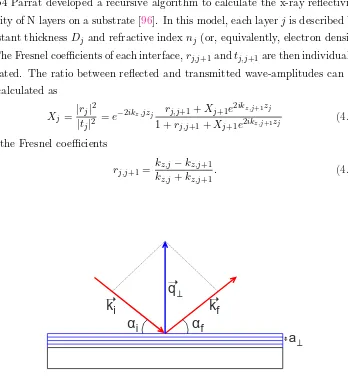
4.2.2 X-ray reflectivity . . . 38
4.2.3 Parrat formalism . . . 39
4.2.4 Grazing incidence diffraction . . . 40
4.3.1 Complex reflectance ratio . . . 43
4.3.2 Complex dielectric tensor . . . 45
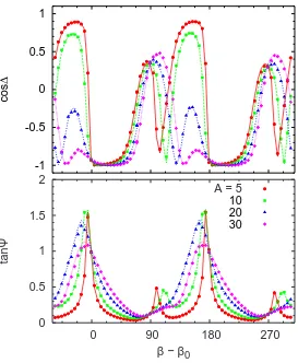
4.3.3 Anisotropic materials: Theβ−scan method . . . 46
4.4 Raman scattering . . . 48
5 F16CuPc thin films 51 5.1 Isotropic F16CuPc thin films on SiO2 . . . 52
5.1.1 Morphology and structure . . . 52
5.1.2 Optical Properties . . . 59
5.2 Films of F16CuPc on MgO . . . 61
5.3 F16CuPc thin films on Al2O3 . . . 62
5.3.1 Structure and morphology . . . 63
5.3.2 Optical properties . . . 68
5.4 Raman scattering on F16CuPc thin films . . . 73
5.4.1 Differences in the spectra of films on different substrates . . 76
5.4.2 Symmetry considerations . . . 76
5.4.3 Mode assignment . . . 80
5.4.4 Angular dependence of the intensities . . . 82
5.4.5 Davydov splittings . . . 87
5.5 Influence of the growth conditions . . . 91
5.5.1 Growth at different deposition temperatures . . . 91
5.5.2 Growth at different layer thicknesses . . . 96
5.6 Conclusions . . . 97
6 DIP thin films 101 6.1 DIP thin films on SiO2 . . . 102
6.1.1 Structure of DIP films on SiO2 . . . 103
6.1.2 Optical properties . . . 108
6.2 DIP thin films on Al2O3 . . . 112
6.2.1 Morphology . . . 112
6.2.2 X-ray Diffraction . . . 115
6.2.3 Growth . . . 119
6.2.4 In-plane structure . . . 121
6.2.5 Optical constants . . . 124
6.3 Conclusions . . . 130
7 Organic heterostructures 133
7.1 DIP on F16CuPc films . . . 134
7.2 F16CuPc on DIP films . . . 137
7.3 Conclusions . . . 140
8 Summary 141
8.1 Thin films on SiO2 and MgO . . . 141
8.2 Thin films on Al2O3 . . . 143
8.3 Organic heterostructures . . . 144
A Al2O3 substrates 145
B Unit cell determination of F16CuPc 149
C Angular dependence of Raman intensities 157
List of Figures 159
List of Tables 165
List of Symbols 167
List of Acronyms 171
Bibliography 173
Acknowledgments 187
Index 189
Introduction
Semiconducting organic materials have attracted interest during the last decades due to their interesting optoelectronic properties. Their application in new flexible
and transparent devices [1, 2], their tuning possibilities, and a potential low cost in the manufacturing lead to an increase of the academic activity in this field. The
advances in the last decade attracted also the interest of the industry, and many companies have nowadays their own development division working on the field of organic electronics. At present, many applications of organic semiconductors
have been demonstrated [3], and several devices that use organic semiconducting materials can already be found in the market. Although those materials
can-not compete in performance with the traditional inorganic semiconductors (with charge carrier mobilities several orders of magnitude higher), they can be used in innovative applications such as large-area light emitting devices, on flexible
substrates [2] or when low cost is required.
Organic materials with semiconducting properties can be classified into two big groups, polymers and low-weight organic molecules [4]. In particular,
low-weight organic molecules show very interesting optoelectronic properties for the development of new applications as transparent devices, waveguides, large-area
flat displays [5, 6], or organic solar cells [7, 8]. In contrast to polymers, small organic molecules form ordered crystalline structures. The close packing of the molecules in the solid enhances the π-orbital overlap in the material, origin of
its semiconducting and transport properties [9, 10]. Hence, similarly to the con-ventional inorganic semiconductors, in order to improve the electronic properties
of the material highly ordered structures are required [1, 11, 12]. Moreover, the
combination of different type of organic molecules is needed in the development
of some devices such as organic solar cells, or organic light-emitting diodes, where at least two organic layers are combined. Therefore, a comprehensive survey of the organic-organic interface is crucial for technological applications.
The use of molecular beam epitaxy for the deposition of organic layers has been an important advance in the study of those systems [11,13,14]. The application of
molecular beam epitaxy in the growth of organic materials has been denoted with the termorganic molecular beam epitaxyor more generallyorganic molecular beam
deposition where no epitaxial relation between the substrate and the overgrown layer is required. The ultra-high-vacuum environment and the well controlled growth conditions this technique offers allow the production of high-quality layers
with an exceptional purity.
However, the growth of organic thin films presents several problems inherently related to the nature of these relatively large molecules. First of all, the unit cells
of these materials are large compared to those of the typical inorganic substrates, and they exhibit a very low symmetry [15, 16]. This frequently leads to the epi-taxial growth of films presenting multiple rotational and translational domains,
since several energetically equivalent orientations of the organic lattice on the in-organic substrate exist. Secondly, the chemical nature of the substrate is crucial.
Strongly interacting substrates usually limit the surface mobility of the molecules during film formation, thus leading to a high density of grains. Moreover,
poly-morphism is favored by the weak intermolecular interactions responsible of the crystal packing. Thus, it is often found that the first few monolayers deposited on the substrate crystallize in a modified structure due to the interaction with
the substrate. Related to this, the morphology of the layer may exhibit different scenarios depending on the growth mode adopted by the layer (Frank–van der
Merwe, Stranski–Krastanov, or Volmer–Weber) [17,18].
In conclusion, situations where the presence of several azimuthal domains, small grain size, and coexistence of different polymorphic forms appear are com-mon in the growth of organic thin layers. Due to these deviations from ideal
growth, the physical properties of the organic layers do not hold compare to their single-crystal counterparts, which can be considered as the upper limit for some
technologically relevant properties such as the charge carrier mobility [1,19].
semiconductors (good hole conducting materials) sincen-type and stable organic
semiconductors are rare [20,21]. However,n−type materials are also needed in the construction ofpn−junctions, as in solar cells [7], and also to implement the well-established complementary logic in organic circuits [22–24]. In this work we study
two organic materials, an n-type compound of the family of the phthalocyanines and a p-type compound, diindenoperylene. Both of them are planar low-weight
molecules.
In this thesis organic films have been grown by organic molecular beam de-position under different growth conditions and on different substrates to study the influence of those parameters on the properties of the layers. We determine
under which deposition conditions the structure of the layers is optimized and which is the influence that the different substrates have on the final structure.
The optoelectronic properties of the films are strongly linked to their degree of structural definition. Therefore, prior to the study of their optoelectronic
proper-ties a full structural characterization is needed. Thus, a multi-technique study of the properties of the films is required. In this work, several techniques allow the independent characterization of the structural and optical properties of layers of
phthalocyanines and diindenoperylene.
The structure of this thesis is as follows. In Chapter2the properties of organic semiconductors are reviewed and the motivation of this work is presented. The
organic compounds studied in this work are also introduced in Chapter2, where a brief summary of the published work on these materials is made. The organic molecular beam deposition technique is described in in Chapter3, where also the
ultra-high-vacuum system used in the growth of the organic layers is introduced. The properties of the substrates used and their preparation are also described in
Chapter3. In Chapter4 the experimental techniques are discussed together with a short introduction to the theoretical background of each of them. Chapters 5
to 7 present and discuss the results obtained in this study. In Chapters 5 and
6 the properties of phthalocyanine and diindenoperylene layers on the different substrates used are presented. It is shown that different degrees of structural
ordering in the layers are obtained depending on the substrate used and on the deposition conditions. It is shown that the final optoelectronic properties of the
heterostructures combining both compounds (phthalocyanine and
diindenopery-lene) are shortly discussed, and some of the problems that may arise from the complexity of these interfaces are emphasized. Finally, in Chapter 8 we sum-marize the main results obtained. Special emphasis is made on the relationship
Organic semiconductors
The present chapter is devoted to organic compounds which present semicon-ducting properties. Asorganic compounds we consider those materials containing
basically carbon, in association with hydrogen, oxygen, and nitrogen. The unique chemistry of carbon allows the construction of very complex molecular structures,
and the possibility to combine them with many other different atoms or atomic groups. This rich variety of structure and electronic properties that organic com-pounds offer is probably the most attractive advantage of these materials. Their
physical properties can be tailored by modifying their molecular structure. The desired optoelectronic properties for a given device can thus be obtained simply
by choosing the appropriate material or by synthesizing a new molecule which meets the requirements needed for a certain application. Furthermore, molecular materials present several other advantages against their inorganic counterparts
which make them suitable for the development of new applications [25,26]. They show very interesting mechanical properties and are suitable for the fabrication of
low-cost electronic circuits.
This chapter is organized as follows. In Section 2.1 a short review of the first studies as well as the last developments on organic semiconductors is made. Also
in this section, the basic properties of organic semiconductors are introduced. Sec-tion2.2summarizes the usual problems found in the growth and characterization of thin films of those materials. Section 2.3introduces one of the molecular
com-pounds used in this work, the phthalocyanines. This compound is used as an example to illustrate the main advantages organic semiconductors offer but also
to present some of the problems that need to be solved for the development of
organic devices. Finally, in Section 2.4 the second organic molecule used,
diin-denoperylene, is presented, and a review of the available work on this molecule is made. We should point out that these two materials were already combined to construct an organic solar cell in 1981 [27].
2.1
Basic properties of organic semiconductors
The semiconducting properties of organic compounds are known for nearly one century. Photoconduction in anthracene crystals was discovered in 1906 by
Pochet-tino [28] while its dark conductivity was studied simultaneously with that of silicon in 1910. In spite of these early work, only few papers appeared in the period from
1940 to 1960 [29–31]. In the 1960s the first books and reviews exclusively dedi-cated to organic semiconductors appeared [32–34]. But it has been during the last
three decades when an important increment of the work on this field occurred in many research laboratories followed by an increase of the interest from industry.
Nowadays, several organic-based devices can already be found in the market,
and many major electronics firms as Kodak, Hewlett-Packard, IBM, Philips, Pio-neer, Siemens, or Sony have their own development division working on this field.
Many other new companies appeared (spin-off companies in many cases) dedi-cated exclusively to the production and development of new organic
semiconduct-ing materials (Covion, Dupont Olight, Universal Display Corporation). Organic electronic devices as multicolor automobile stereo displays (Pioneer MEH-P9000) or single OLEDs (Philips shaver 8894XL) appeared in the market during the
last decade. Nowadays, organic materials are being used as full-color displays in devices such as digital cameras (Kodak EasyShare LS633) or mobile phones to
achieve sharp images that are visible from any angle.
Apart from the enormous tuning possibilities of organic compounds, these
mate-rials present many other advantages against their inorganic counterparts. Organic materials, due to the weak intermolecular interactions (van der Waals type) that
held the molecules together, are tough, and can be used to construct new flexible electronic devices. They are also excellent candidates for the production of large-area full-color displays at low-cost using organic light-emitting devices (OLEDs),
which may eventually replace liquid crystal displays and even the standard cath-ode ray tube of our traditional home televisions. Organic circuits fabricated by
personal information, applications in which low-cost rather than high-performance
is required [35,36].
The semiconducting properties of molecular materials can be explained from the covalent bonding between carbon atoms [4]. The electronic configuration of carbon is 1s22s2 2p2. In an organic molecule simple, double, and triple bonds can
be formed between adjacent carbon atoms. Thus, in the benzene (C6H6) molecule
shown in Figure 2.1 each carbon atom forms sp2 σ-bonds with its neighboring
carbon atoms and with one hydrogen atom. It also forms aπ-orbitalperpendicular to the molecular plane.
Figure 2.1: Schematic representation of the π-orbitals in the benzene (C6H6)
molecule, responsible of its semiconducting properties. In the solid, the overlap
betweenπ-orbitals of adjacent molecules will allow the charge transport through the solid.
The interactions in a double bond split the energy levels into a bonding and an anti-bonding molecular π-orbital (see Figure 2.2). The two electrons occupy
the former larger binding energy orbital or highest occupied molecular orbital (HOMO), while the latter remains empty and is called the lowest unoccupied
molecular orbital (LUMO). Optical or thermal excitation can promote an electron to an unoccupied level. For larger molecules further splitting occurs, and finally electronic bands are formed. Intermolecular interactions in the solid lead also
to additional splitting. However, band formation is not sufficient for the organic materials to behave as semiconductors, there must be a mechanism of charge
π-orbitals from one molecule with those of its neighboring molecules. Therefore a
close packing of the molecules and a crystalline structure free of defects is essential to maximize theπ-orbitals overlap and thus improve the conduction properties of the material. The low molecular symmetry leads to highly anisotropic conduction
parameters since the effective path for charge carrier transport is perpendicular to the molecular plane, direction of maximum π-overlap [33]. Thus, parameters
as the charge carrier mobility must be described by a mobility tensor µij [37].
In general, all the physical properties of these materials may present anisotropic
behavior due to the low symmetry of the molecular constituents and the low-symmetric crystalline structures they form.
Figure 2.2: Schematic view of the splitting of the energy levels due to the inter-actions in the π-orbitals of a molecule leads to the formation of the HOMO and LUMO energy bands. Molecular interactions in the solid lead to further splitting
of the molecular orbitals.
2.2
Organic semiconducting thin films
The complexity and anisotropy of the structure of those materials, involving many atoms covalently bonded forming the molecular unit, and van der Waals type forces holding the molecules together in the crystal, complicates their processing
as well as the study of their properties [4, 38]. For the fabrication of electronic devices such as OLEDs [39, 40], organic field effect transistors (OFETs) [41] or
However, the growth of ordered structures in organic thin films has shown many
difficulties related to the nature of these materials [11, 12]. In contrast to conventional inorganic semiconductors thin film growth, where the ad-molecules are usually single atoms with spherical symmetry, for organics each ad-molecule
can involve more than 50 atoms, covalently bonded forming a unit with very low symmetry. The dimensions of these molecular units are in the nanometer
scale, and thus, deposition on inorganic substrates presents lattice mismatches of one order of magnitude [13]. This situation may lead to the appearance of
several energetically equivalent translational domains of the overgrown film. In addition, the complex crystalline structures formed as the molecules crystallize also contribute to the formation of equivalent translational and rotational domains [17].
The interaction with the substrate plays an important role in the final structure of the organic layer. In particular, the balance between the molecule-molecule and
molecule-substrate interactions may lead to completely different growth scenarios. Low-interacting substrates promote molecular diffusion and thus in some cases well-ordered films can be formed. On the other side, strong-interacting substrates
usually limit the surface mobility during film formation, leading to a high density of grains. In general, the interactions between the organic layer and the substrate
are van der Waals type, and therefore physisorption occurs. However, in the extreme case of a highly reactive surface chemisorption may take place, and the
adsorbed molecules may even dissociate. The interaction with the substrate is crucial also in the final morphology of the layer. Finally, the formation of films with several coexisting polymorphic forms is frequently found in organic thin film
growth.
Thus, many structural imperfections as azimuthal disorder, formation of
multi-ple domains, grain boundaries, dewetted morphologies, and also the tendency to polymorphism have to be overcome by appropriately selecting all the parameters
that influence the growth of the layers [43]. Those concern not only the growth conditions (as substrate temperature, thickness, and growth rate), but also the reactiveness, morphology, and symmetry of the substrate surface. In addition, in
organic heterostructures, needed in many applications as OLEDs or organic solar cells, other issues related with the complex organic-organic interface may appear.
2.3
Phthalocyanines
The wordphthalocyanine comes from the combination of two Greek terms which perfectly define the colorful properties of this material, these are naphtha (rockoil)
and cyanide (dark blue). This material is a blue dye known for many years. The first phthalocyanine was produced accidentally in 1907, when Braun and
Tcherniac observed the precipitation of a highly insoluble product on heating an alcoholic solution of a benzamide [44]. Linstead and coworkers determined in the 1930s the molecular structure of the phthalocyanines [45], and showed
that the different phthalocyanine derivatives known fitted in the molecular scheme shown in Figure 2.3. The parent compound, hydrogenated phthalocyanine, with
chemical formula C32H18N8, has 2 hydrogen atoms in the center of the ring, and 16
surrounding the molecule. Later on, Robertson determined the crystal structure
of several phthalocyanines by x-ray diffraction measurements [46–48].
Phthalocyanines were also involved in the origin of the interest on the semi-conducting properties of organic solids in 1948, when Eley and Vartanyan studied their conductivity. Nowadays, they are one of the best studied systems in
or-ganic chemistry, and several text books devoted exclusively to their chemistry and physical properties have been published [49,50].
Phthalocyanines and particularly metallo-phthalocyanines [42] (where the two central hydrogen atoms have been substituted by a metallic atom) present very
interesting properties which make them an excellent example to illustrate the advantages organic materials offer. Phthalocyanines are easily sublimed and can be crystallized with an exceptional purity. They are highly stable and do not show
degradation up to temperatures above 400◦C. They are not affected by strong acids or bases [50]. Phthalocyanines show very interesting optical properties. The
conjugated π-system, containing 18 electrons in the macrocyclic ring, leads to very intense absorption bands in the visible [49]. Their bluish colorful appearance
arises from the presence of a strong absorption band at the red end of the visible spectrum, near 670 nm.
Several thousands of tons of phthalocyanine are produced every year. Due to their intense coloring properties, they are used as pigments in many industrial
paints (as car paintings) or in inks for color laser printers, they are also used as the data storage layer of many CD’s we use every day [51]. Their sensitivity to ambient
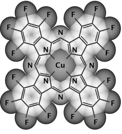
Figure 2.3: Schematic representation of the molecular structure of F16CuPc with
chemical formula C32F16N8Cu. Other phthalocyanine derivatives have similar
structures. The parent compound has 16 hydrogen surrounding the molecule and two hydrogen atoms in the center.
change of conductivity of the material upon gas absorption [52]. They are a very versatile system, more than 70 different phthalocyanines have been synthesized
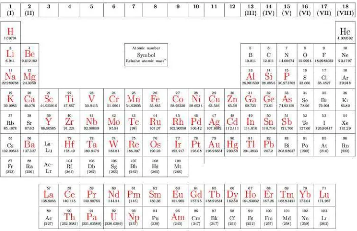
only by changing the central atom. Phthalocyanines containing in the center of the ring the different atom species highlighted in the periodic table of Figure2.4
have been produced [49]. The replacement of the central atom slightly modifies the electronic properties of the material [50, 53], while its molecular structure is, in most cases, unchanged.
Among all phthalocyanine derivatives, copper-phthalocyanine (CuPc) is one of the most studied derivatives, and was one of the first metallo-phthalocyanines to be synthesized in 1927. The compound used in this work is copper
hexadecaflu-orophthalocyanine (F16CuPc), in which the 16 hydrogen atoms surrounding the
molecule have been substituted by fluorine, having thus a molecular weight of
Figure 2.4: More than 70 different phthalocyanines have been synthesized only by changing the central atom. Apart from the parent compound (C32H18N8),
having two hydrogen atoms in the center, phthalocyanines having in the center of the ring the highlighted atoms in the periodic table (more than 70) have been synthesized.
becomesn-type upon fluorination. This is an excellent example of how the mod-ification of the molecular structure can change the properties of the material. In
fact, F16CuPc is one of the most stable n-type organic semiconductors known at
present, and it has been used to construct the first n-channel organic transistor
[54], in complementary logic organic circuits [35, 55, 56], and also in paper-like electronic displays [36].
The first study of the structure of several phthalocyanines was reported by Robertson in 1935 [46]. Monoclinic structures with the space group P21/a (C25h
or 14:b3) were reported for the metal-free, nickel-, copper- and platinum deriva-tives, with two molecules per unit cell in all cases. The results on the metal-free
published on the copper derivative by Brown [58], who obtained similar results
for the cell parameters. The values reported are shown in Table 2.1. CuPc and other phthalocyanines crystallize forming long and narrow needles (up to 1 cm length but only 0.1 cm × 0.01 cm wide). The long axis of the needle coincides with the b-axis of the monoclinic structure [46, 58]. In Figure2.5 the packing of the molecules in the unit cell ofβ-CuPc is shown. Figure2.5(a) shows the packing
on the ac-plane of the crystal, while Figure2.5(b) shows theab-plane.
(a)
c
a
(b)
[image:27.595.190.432.284.553.2]b
Figure 2.5: Packing of the molecules in theβ-CuPc structure reported by Robert-son [46]. (a) Projection on theac-plane and (b) projection on theab-plane, where the unique monoclinicb-axis points in the viewing direction in (a) and is aligned vertically in (b).
In thin films of various phthalocyanines, two structural phases have been re-ported, a metastable α and a stable β forms [59]. The growth of the α-form is
H2Pc [46] H2 Pc [57] β-CuPc [46] β-CuPc [58] F16CuPc [62]
M 514.55 514.55 575.67 575.67 863.9
Space group P21/a P21/a P21/a P21/a P21/a
a(˚A) 19.85 19.870 19.6 19.407 20.018
b (˚A) 4.72 4.731 4.79 4.79 5.106
c (˚A) 14.8 14.813 14.6 14.628 15.326
β 122.25◦ 121.98◦ 120.60◦ 120.56◦ 111.83◦
U (˚A3) 1173 1181 1180 1166 1454
Z 2 2 2 2 2
Table 2.1: Cell parameters reported for metal-free and copper-phthalocyanine by Robertson [46], Brown [58], and Matsumoto [57]. In the last column we show also the unit cell parameters of the compound F16CuPc, derived from powder
diffraction measurements (AppendixB).
transition temperature during growth [60]. Irreversible phase transformations can be induced by a thermal treatment [61]. Other polymorphic structures of CuPc
asγ-,δ-, andχ-modifications have been also reported [42].
The crystal structure of F16CuPc does not appear in the literature. However,
its powder spectrum shows similar lines to that of the CuPc. From the powder spectra the unit cell constants shown in the last column of Table2.1can be derived
[62], details on this study can be found in AppendixB. A similar crystal structure to that of the CuPc with an expanded unit cell is obtained. The larger values of
the unit cell parameters can be related to the substitution of the hydrogen atoms surrounding the molecule by fluorine.
2.4
Diindenoperylene
The second organic molecule studied in this work isdiindenoperylene (DIP), also referred as periflanthene. The molecular structure of DIP is shown in Figure2.6.
It is also a planar molecule, formed by a perylene core with two indeno groups, with chemical formula C32H16. Its molecular weight is 400.48 g/mol and has a
sublimation point above 350◦C in vacuum. Its molecular dimensions are 18.4 ˚A along the long axis and 7 ˚A along the short axis calculated according to the Cambridge crystallographic database [63]. It is a red dye first synthesized in 1934
Figure 2.6: Schematic view of the molecular structure of a DIP molecule with chemical formula C32H16.
it only contains carbon and hydrogen, and a total of 48 atoms, against the 57 atoms that conform the F16CuPc molecule. However, the molecular symmetry is
lower in DIP, which hasD2h symmetry.
In contrast to the huge amount of published work on phthalocyanines, there are
very few studies on DIP available. Besides the published reports on its synthesis [64, 65], it was not until 1951 that several studies reporting powder diffraction
measurements on DIP appeared [66–68]. However, the bulk crystal structure of DIP was not known until recently when Pflaumet al.determined a triclinic struc-ture by x-ray diffraction measurements on DIP single crystals [69]. Nevertheless,
other crystalline structures have been reported from studies of thin films of DIP on several substrates, which differ from its bulk structure [70]. The reported unit
cell parameters are summarized in Table 2.2. Thus, the DIP crystal structure of DIP thin films is not yet well-established. From the reported studies it is
appar-ent that it differs from the bulk phase. Recappar-ently, detailed studies on the structure [71] and the conduction properties [63] of DIP thin films on SiO2 appeared. It
was shown that three different structural phases can be observed in thin films. A
Pflaum,Frey & Karl Hoshinoet al. Hoshinoet al.
Single crystal DIP/NaCl DIP/Perylene
Triclinic Monoclinic Monoclinic
a(˚A) 11.59 8.67 11.0
b(˚A) 12.97 6.96 10.6
c(˚A) 14.88 18.55 17.5
α 98.11◦ 90.0◦ 90.0◦
β 98.10◦ 93.5◦ 106.0◦
γ 114.53◦ 90.0◦ 90.0◦
Z 4 2 2
Table 2.2: Several DIP crystal structures determined on single crystals and thin films. The triclinic structure has been determined in DIP single crystals by Pflaum
et al., with four molecules per unit cell and P1 symmetry [69]. Different
crys-talline structures in thin films with monoclinic symmetry have been reported by Hoshino [70].
modifications are irreversible, and thus the changes are maintained when the tem-perature is lowered again. At temtem-peratures above 160◦C desorption of the DIP layers starts [71].
DIP thin films have shown very interesting conduction properties, which have been related to the high structural definition (particularly to the low mosaicity
measured by x-ray diffraction) of the layers [63]. Very interesting structural results have been recently reported [71] for DIP layers on oxidized silicon wafers. It has been shown that highly ordered films can be obtained, with mosaicities narrower
than 0.01◦ as probed by x-ray diffraction. The high degree of order of those organic layers was also observed by cross-sectional TEM (transmission electron
microscopy) measurements, which allowed the resolution of individual molecular monolayers [72]. Despite the good structural quality of the layers, it has been
shown that their roughness increases rapidly with thickness [73]. DIP has been also used in studies of the metal-organic interfaces. Particularly in the study of the thermal stability of Au contacts on DIP layers [74], and DIP thin films on
polycrystalline Au [75]. DIP has been also used to determine the effects induced in the organic films by the deposition of insulating layers of aluminum oxide on
The exceptional degree of order found in DIP thin films on oxidized silicon
has been one of the main reasons to choose this material in the present work. Moreover, DIP is a p-type organic semiconductor, and thus complementary to the other organic compound studied here, F16CuPc. As we already mentioned,
Organic
Molecular Beam Epitaxy
In this chapter we introduce the deposition technique ofmolecular beam epitaxy
(MBE) used for the growth of the organic thin films studied in this work. MBE is a technique used for the production of high-purity layers based on the evaporation
of material in a ultra-high vacuum (UHV) environment. Heated sources produce the molecular or atomic beams that react with the substrate surface, which is
maintained at a desired temperature. Compared to other evaporation techniques, MBE offers a higher level of control on the growth conditions, especially on the beam fluxes. Growth rates below 1 ML/min can be easily achieved by control
of the temperature of the evaporation sources. The use of beam blocking shut-ters allows the deposition of complex heterostructures with sharp interfaces. In
addition, the UHV conditions provide an environment free of contaminants.
The contents of this chapter are organized as follows. In Section 3.1 the gen-eral concepts of the MBE technique are introduced and the advantages it offers
against other evaporation techniques are discussed. Specific issues related with the application of MBE in the growth of organic layers are also emphasized in Section 3.1. In Section 3.2 some general aspects of thin film growth relevant in
this study are addressed. In Section3.3the different parts of the UHV equipment used in this work are described. Finally, in Section3.4the main characteristics of
the substrates used, as well as their preparation procedure are explained.
3.1
MBE and OMBE
MBE is a technique used for the epitaxial growth of materials. It is based on the reaction between a molecular or atomic beam and a substrate maintained at the
desired temperature (Tg) under UHV conditions [77]. The molecular beams are
usually generated at sources asKnudsen cells or electron beam evaporators, where
the constituent materials are evaporated.
MBE was first used in the late 1960s in the growth of GaAs layers and it has been successfully applied in the epitaxial growth of many inorganic semiconductors
as well as in the growth of metal or insulating layers. MBE presents several advan-tages against other epitaxial growth techniques. Due to the UHV environment in which the growth is realized, epitaxial layers with an extremely high purity can be
obtained. In addition, this technique offers a high degree of control on the growth parameters. The beam fluxes can be precisely controlled by the temperature of
the source. The molecular beams can be individually blocked by beam shutters, and therefore complex heterostructures with atomically sharp interfaces can be
produced [78]. Very low rates can be achieved by controlling the temperature of the source. The high control over the beam flux allows the reproducible deposi-tion of layers at the submonolayer regime and the “in-situ” study of the growth
process at a processable time-scale. Moreover, the UHV environment admit the use of characterization techniques as electron diffraction (LEED and RHEED) or
Auger electron spectroscopy, techniques which are useful not only for the charac-terization of the overgrown films, but also for the control of the substrate surface before deposition, and for growth-monitoring.
The application of MBE in the growth of organic materials has been an
impor-tant advance for the controlled growth of high-purity organic layers [14]. The first reported study of the MBE growth of an organic compound was by Haraet al. in
1989 [79]. They reported the growth of CuPc layers on MoS2. After this early
work many reports and reviews on the application of MBE in organic thin film
growth appeared [13,15,80], and the technique was referred to asorganic molecu-lar beam epitaxy (OMBE). The termorganic molecular beam deposition (OMBD) became more frequently used since epitaxy of organic thin films on inorganic
sub-strates, with an epitaxial relation between the lattices of the deposited layer and the substrate, does not always occur. OMBD can be applied to “small molecules”
organic materials are normally Knudsen cells. The low sublimation temperatures
of organic materials (usually between 100 and 500◦C) simplifies the design of the sources.
The main differences between inorganic and organic MBE originate from the dis-tinct nature of the molecular constituents. While in inorganic MBE the units are
frequently single atoms, in OMBD complex molecules are used. These molecules are extended objects with very low symmetry [11,16]. As we briefly addressed in
Chapter 2, the dimensions of the molecules and the unit cells in which they crys-tallize are larger than the inorganic substrates, and their symmetry is lower. This large lattice mismatch between substrate and organic layer leads to several
possi-ble translational and orientational domains of the organic lattice on the substrate.
A second important difference between inorganic and organic MBE is the weaker interactions involved in the growth process of organic materials. The
molecule-molecule as well as molecule-substrate interactions are usually van der Waals type. The termvan der Waals epitaxy has been used to refer to epitaxial
organic thin films [80] on low-interacting surfaces. Also, the usual temperatures involved in OMBE are lower than in inorganic MBE due to the weaker character of these van der Waals forces [11].
Despite the last developments in the growth of ordered organic layers [81], there
are still many problems which have to be solved before we can profit of all the interesting properties of organic semiconductors [12]. Probably one of the most
attracting properties of these materials is their intrinsic anisotropy [82,83]. How-ever, due to structural disorder, thin films of those materials present commonly isotropic properties [84]. OMBD offers the path for the optimum control of the
growth conditions in a clean environment free of contaminants [11,81]. The under-standing of the influence of the substrate surface, and in particular its reactiveness
and morphology, on the growth of the organic layer is crucial to achieve control on the growth process.
3.2
Thin Film growth
The process of thin film growth takes place at the substrate surface, where the
(1)
(4)
[image:36.595.117.457.108.363.2](3)
(2)
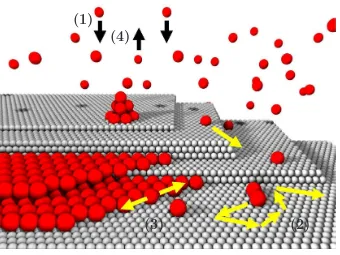
Figure 3.1: Surface processes occurring during film formation in MBE. (1)
adsorp-tion, (2) surface migraadsorp-tion, (3) incorporaadsorp-tion,and (4) desorption. Figure taken from reference [18].
of the impinging molecules occur. This situation is illustrated in Figure3.1.
Sev-eral surface processes are involved in the growth, the most important, exemplified in Figure 3.1are
• adsorption of the impinging molecules on the surface,
• migration and dissociation of the molecules along the surface,
• incorporation of the molecules in crystal sites of the substrate or of the overgrowing layer,
• desorption.
Thus, when a molecule hits the surface, it can migrate before it finds an
incorpo-ration site or it can meet a second molecule to form a dimmer. This dimmer can dissociate or can increase its size by the incorporation of other molecules. Finally,
All these kinetic processes are quantitatively described by several growth
pa-rameters. First of all, themolecular flux Fi describes the number of molecules of
the constituent i impinging on the substrate surface. This flux is determined by the source temperatureTi. Ti also determines the energy of the molecules arriving
on the surface, which is maintained at a temperature Tg (Tg < Ti). The fraction
of molecules which are incorporated, will interact with the substrate until
thermo-dynamic equilibrium is reached at the temperatureTg. The molecules which are
not incorporated, and therefore are desorbed, will leave the surface with an
en-ergy corresponding to the temperatureTe. We can now define anaccommodation
coefficient as
a= Ti−Te
Ti−Tg
(3.1)
which is a measure of the level of thermal equilibrium reached by the arriving
atoms with the substrate. Thus, a = 1 when Te = Tg. A second parameter
frequently used is thesticking coefficient (also referred as condensation coefficient)
of the molecules as
s= Nad
Ntot
(3.2)
whereNadis the number of adsorbed molecules andNtotis the number of molecules
arriving on the surface. Thus, s is the probability that one atom or molecule impinging on the surface sticks. For high substrate temperatures, the sticking
coefficient may have very low values, and even s = 0 for sufficiently high Tg.
However, all the arriving atoms can be accommodated on the surface, and therefore
a= 1, and then gain sufficient energy to leave the substrate.
The adsorption of a molecule on a surface is usually described by a two step process. First, physisorption takes place, where the involved attracting forces are
van der Waals type. The second step is chemisorption, in which electron transfer occurs. Usually two sticking coefficients are defined, one for each type of
adsorp-tion. For the molecules and substrates used in this study, only physisorption of the adsorbates takes place. However, due to the distinct nature of the inorganic substrate and the organic layer, different sticking coefficients have to be defined
for the first deposited organic monolayer (organic on inorganic sticking coefficient,
so−i) and for the subsequent deposited material (organic on organic sticking
The interaction of the film with the substrate may also lead to different
mor-phologies of the overgrown layer. There are three possible growth modes of a crystal on a surface [85] depicted in Figure 3.2. In Frank-van der Merwe growth or layer-by-layer growth (Figure 3.2(a)), the first atoms or molecules on the
sur-face form a closed monolayer on the substrate before the second monolayer starts to nucleate. The subsequent layers continue with the same behavior. The growth
mode illustrated in Figure 3.2(b) is called Stranski-Krastanov or layer plus is-land. In this case the early stages of the growth are similar to the layer-by-layer,
since the first monolayers are closed. However, once a certain critical thickness is reached, islands are formed on top of these first closed layers. Finally, in the third growth mode (Figure 3.2(b)), called Volmer-Weber or island growth, small
clusters nucleate on the substrate surface and grow forming islands.
(a)
(b)
(c)
Figure 3.2: Schematic representation of the growth of a layer in (a) Frank-van
der Merwe (layer-by-layer), (b) Stranski-Krastanov (layer plus islands), and (c) Volmer-Weber (island) the different growth modes. Extracted from reference [85].
In general, layer-by-layer growth takes place when the interaction of the
ad-molecules with the substrate is stronger than the interaction between ad-ad-molecules. Island growth is found in the opposite case, that is, when the interaction be-tween ad-molecules predominates. Finally, the intermediate case, layer plus island
growth, can be originated by several reasons. For instance, in situations where the lattice parameter or molecular orientation of the first monolayers can not be
3.3
UHV system
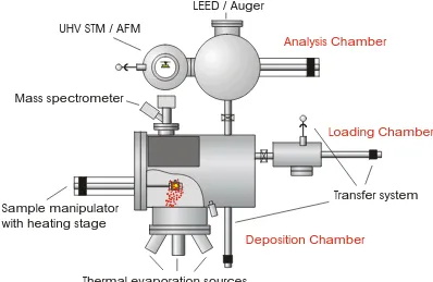
The UHV system used in this study for the deposition of the organic layers is a commercial Omicron system composed of three chambers. An schematic view of
the system is shown in Figure 3.3. A small fast entry load-lock chamber allows the introduction and extraction of samples without breaking the vacuum of the
main chambers. This chamber is provided with a sample storage stage, which is equipped with a heating station. This station has a ceramic heater for tempera-tures up to 500◦C, and four additional positions for sample storage. This heating station is specially useful for the outgassing of the substrates before introduction to the MBE system, thus unnecessary contamination of the growth chamber is
avoided. A transfer rod allows the transportation of samples from this chamber into the MBE deposition section.
The MBE chamber is equipped with four Knudsen cells for the evaporation of
UHV STM / AFM
LEED / Auger
Loading Chamber Analysis Chamber
Deposition Chamber
Mass spectrometer
Thermal evaporation sources Sample manipulator
with heating stage
[image:39.595.115.513.363.622.2]Transfer system
Figure 3.3: Schematic top view of the UHV system used for the evaporation of the organic layers. The system is composed by a growth chamber, an analysis chamber
and a fast entry load-lock chamber. A transfer system allows the transportation of samples between the different chambers without breaking the vacuum (from
materials and a quadrupole mass spectrometer (QMS) which can measure up to
1000 a.u. and thus detect the presence not only of the residual gases but also of the molecular materials evaporated from the Knudsen cells. The base pressure of this section of the system is about 5×10⁻¹⁰ mbar. During growth the deposition
rate and thickness are monitored using a quartz crystal microbalance (QCM). On the sample manipulator of this chamber the sample can be heated up to 800◦C, or cooled down by using liquid-nitrogen. The pressure during growth can be further reduced by using a liquid-nitrogen cooled cryo-shroud.
In the analysis chamber, an AFM system (AFM/STM Omicron system) allows the in-situ surface characterization of the films. The samples can be transferred from the growth stage to the AFM without breaking the vacuum. Also in the
analysis chamber LEED and Auger spectroscopy can be performed. The sample can also be heated up to 800◦C in this chamber. The base pressure of this section is 5×10⁻¹¹ mbar.
The system is pumped by a turbo-molecular pump which can be used to pump separately the three chambers, two ion-pumps (one in the MBE and one in the
analysis chamber) and two titanium sublimation pumps complete the vacuum generation system.
3.4
Substrates used
As substrates for the deposition of the organic layers, three different oxides have been used, i.e., oxidized silicon wafers, single-crystalline Al2O3 (sapphire), and
MgO. Since all three substrates are oxides, their interaction with the molecules is van der Waals type and therefore no chemical reaction is expected. However,
as described below, their surface is very different due to their different crystalline structure, with considerably different morphologies.
Oxidized silicon substrates were chosen as substrates since they are well-known and widely used in the growth of thin films, they can be easily cleaned and present
an atomically flat surface. Si(100) with native oxide (∼ 3 nm) was used. In contrast to the highly reacting clean silicon surface, where diffusion of the ad-molecules is blocked, the oxide layer allows the migration of ad-molecules thus favoring
the formation of well-ordered films. Moreover, oxidized silicon is technologically interesting since the oxide layer serves as the insulating layer between the Si
construction of an organic transistor.
Al2O3 single crystalline substrates are obtained in a highly pure form
(corun-dum and sapphire) and its crystalline structure [86] and surface [87] are well-characterized. Although Al2O3 is rhombohedral, it is commonly described in
terms of hexagonal Miller-Bravais indices [88]. For details on the crystal structure
and morphology of the Al2O3 substrates we refer to Appendix A.
The sapphire substrates used in this study are A-plane oriented, or Al2O3
(1120). In this orientation, the c-axis of the substrate is in the surface plane, and thus is a two-fold symmetry surface having a rectangular unit cell on the plane. The surface of the as obtained substrates has been mechanically polished.
After this polishment procedure it is disordered and presents roughnesses around 2-5 nm. An annealing treatment can be used to reorganize the surface and obtain
an atomically flat substrate. Thus, before introduction in the UHV chamber, the substrates are annealed in air at temperatures above 1000◦C. After this annealing treatment the surface is characterized by the formation of atomically flat terraces that correspond to the (1120) low-index plane. The terraces appear to account for the small misalignment between the physical surface and the crystallographic
A-plane. The magnitude and orientation angles between these two surfaces, the so called miscut angle, can be easily determined with high accuracy by x-ray
diffraction measurements. The magnitude and orientation of the miscut, together with the temperature and duration of the annealing process, will determine the
morphology of the substrate. In AppendixAwe give further details and examples of the morphologies obtained under different conditions.
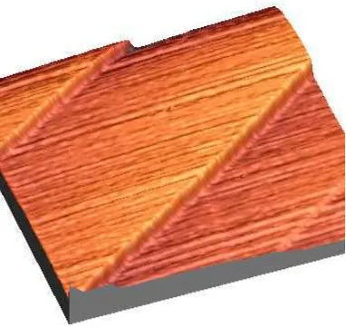
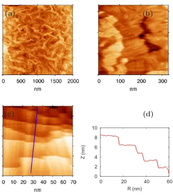
In Figure 3.4 an AFM image of the surface of the substrate before growth is
shown. In this case, the substrate has a miscut of 0.26◦ and an orientation of 49◦ from the c-axis. The annealing treatment was performed at 1400◦C during 15 hours. This lead to terraces of 130 nm wide and 1.8 nm step height. The
surface of the terraces is atomically flat, and is the plane (1120) or A-plane of the Al2O3.
Finally, MgO (100) substrates have also been used in this study. MgO has a
cubic bulk structure with a = 4.203 ˚A. The morphology of the substrates used is shown in Figure 3.5. As can be seen in this AFM image, the surface exhibits
Figure 3.4: AFM image (1×1 µm) of the surface of the Al2O3 substrates before
growth. The terrace surface corresponds to the (1120) planes of the substrate. The step height is around 18 ˚A. The substrate has been annealed at 1500◦C during
18 hours.
image is σrms = 3 nm and therefore relatively high compared to the other
sub-strates used.
The cleaning procedure used to obtain a contamination-free surface of the dif-ferent substrates used is as follows. SiO2 substrates have been cleaned in ethanol
and dried with a stream on nitrogen. Al2O3 and MgO have been cleaned by
suc-cessive ultrasonic baths with organic solvents (acetone and ethanol). Prior to film growth, all the substrates have been kept at 750◦C for at least 12 hours in UHV for outgassing. After these procedures the surface of all substrates is free of any contaminant as probed by AFM measurements performed just before deposition
Experimental techniques
In the present chapter we describe the different techniques utilized to characterize structurally and optically the organic layers. The goal of this work is to
deter-mine the influence of the growth conditions in the structural properties of the layers and to establish their influence in the final optoelectronic properties of the organic films. This is only possible by the combination of techniques of different
areas, which independently characterize the structural and optical properties of the films. Thus, this is a multitechnique study using several techniques which
provide information on the morphology, the crystalline structure, and the optical response of the layers. The techniques used are atomic force microscopy, x-ray
diffraction, spectroscopic ellipsometry and Raman scattering. The combination of all those different techniques allows a better understanding of the properties of the organic layers. While atomic force microscopy bears information on the
morphology of the layers and on their in-plane structure at the nanometer to micrometer scale, x-ray diffraction probe the crystalline structure of the layers
in a macroscopic scale. The comparison of the structural results obtained with these techniques with the Raman scattering data, permits a better understanding
of the molecular packing and ordering in the layers. Furthermore, ellipsometric measurements allow the location of electronic transitions and the quantification of the anisotropy of the layers, which is related with the degree of structural order
present. With the interdisciplinary nature of this work we aim to a better under-standing of the interrelation between the structural and optical properties of the
organic layers.
In Section4.1we present the details on the atomic force microscope used to
char-acterize the morphology of the substrate used and also of the overgrown layer. In Section 4.2 the basic principles of x-ray scattering are presented together with the different geometries used for the structural characterization of the layers, and
also the theoretical methods used to interpret the results. In Section4.3, spectro-scopic ellipsometry is introduced. In this section the experimental aspects of the
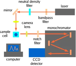
measurement are presented. Finally, Section4.4introduces the Raman scattering technique.
4.1
Atomic force microscopy
4.1.1 Scanning Probe Microscopes
The invention of the scanning tunneling microscope (STM) in 1985 [89] and the
atomic force microscopy(AFM) in 1986 [90] by Binniget al.1 redefined the concept of microscopy and gave rise to the new family of instruments known as scanned probe microscopes (SPMs). SPMs are instruments used in the study of the surface
properties of materials at the atomic to micron level. Although all SPMs contain some common components, they can work in a still growing list of different modes
which probe different properties of the surface. Thus, STM, the first instrument to atomically resolve real-space images of surfaces [89], is based on the measurement of a current that “tunnels” from a sharp conducting tip which probe the surface
of a conducting sample. AFM has become one of the most popular SPMs. In an AFM, a very sharp tip of few microns long and often less than 10 nm in diameter
is located at the free end of a cantilever. The cantilever deflection is measured as the tip is scanned over the sample (or the sample is scanned under the tip, as is
the usual case). The measured deflection allows to generate a map of the surface topography. AFM measurements can be performed on conducting samples as well as on semiconductors and insulators. Other SPMs, as magnetic force microscope
(MFM), scanning near-field optical microscopy (SNOM) are some examples of the many SPMs which use different interactions to probe different properties of
the surface. AFM and STM are also used to modify the surface properties of the sample in nanolithography. These techniques can change the surface by modifying
it atom by atom.
1
4.1.2 Design and operation of an AFM
Most of the SPMs use the same elements to control the sample and the tip, however
we concentrate on the usual components of an AFM. Usually the sample is scanned under the tip driven by a piezoelectric material that changes its dimensions in
response to an applied voltage. A segmented tube design allows movement in the
xy-plane (surface plane) as well as in thez-axis (perpendicular to the surface). The deflection of the cantilever as the sample is scanned is usually detected by optical
techniques. A laser beam reflected on the free end of the cantilever is focused on a position-sensitive photodetector (PSPD) by using one or more mirrors. This
setup allows the precise detection of small vertical displacements of the cantilever (in the sub-˚angstr¨om scale), as well as lateral deflection of the cantilever (using a
four quadrant PSPD). All these components are shown in Figure4.1. In addition, the associated electronics allow the control and alignment of the different parts of the instrument, while the measured data is acquired by a computer.
PSPD PSPD PSPD PSPD PSPD
Figure 4.1: Schematic of a tip scanning a surface in an AFM. A laser beam reflected on the free end of the cantilever is focused on a four-quadrant PSPD. This allows
the precise detection of small cantilever deflections.
AFM measurements can be performed in two different modes which differ on the
distance between the tip and the surface of the sample. The cantilever deflection is due to the forces between the tip and the surface of the sample as their relative
![Figure 2.5: Packing of the molecules in the βthe unique monoclinicson [-CuPc structure reported by Robert-46]](https://thumb-us.123doks.com/thumbv2/123dok_es/5326949.98905/27.595.190.432.284.553/figure-packing-molecules-unique-monoclinicson-structure-reported-robert.webp)