Polycrystalline thin films of antimony selenide via chemical bath
deposition and post deposition treatments
Y. Rodrı´guez-Lazcano, Yolanda Pen˜a, M.T.S. Nair *, P.K. Nair
Department of Solar Energy Materials, Centro de Investigacio´n en Energı´a, Universidad Nacional Auto´noma de Me´xico, Temixco, Morelos-62580, Me´xico
Received 31 December 2004; received in revised form 8 July 2005; accepted 18 July 2005 Available online 18 August 2005
Abstract
We report a method for obtaining thin films of polycrystalline antimony selenide via chemical bath deposition followed by heating the thin films at 573 K in selenium vapor. The thin films deposited from chemical baths containing one or more soluble complexes of antimony, and selenosulfate initially did not show X-ray diffraction (XRD) patterns corresponding to crystalline antimony selenide. Composition of the films, studied by energy dispersive X-ray analyses indicated selenium deficiency. Heating these films in presence of selenium vapor at 573 K under nitrogen (2000 mTorr) resulted in an enrichment of Se in the films. XRD peaks of such films matched Sb2Se3. Evaluation of band gap from optical spectra of such films shows absorption due to indirect transition occurring in the range of 1 – 1.2 eV. The films are photosensitive, with dark conductivity of about 210 8(Vcm) 1and photoconductivity, about 10 6(Vcm) 1under tungsten halogen lamp illumination with intensity of 700 W m 2. An estimate for the mobility life time product for the film is 410 9cm2V 1. D2005 Elsevier B.V. All rights reserved.
PACS:68.55.Nq
Keywords:X-ray diffraction; Chemical deposition; Antimony selenide; Photoconductivity
1. Introduction
Antimony(III) selenide has a ribbon-like polymeric structure in which each Sb-atom and each Se-atom is bound to three atoms of the opposite kind that are then held together in the crystal (orthorhombic, a = 11.62 A˚ , b = 11.77 A˚ , c = 3.962 A˚ ) by weak secondary bonds[1]. Optical band gaps due to both direct and indirect transitions in the range of 1 to 1.13 eV and thermal energy gap of 1 – 1.32 eV are reported for the material[1,2]. This makes it suitable for use as an absorber material in polycrystalline thin film solar cells [3]. A photoelectrochemical solar cell, employing antimony selenide thin film as photoanode, has shown short-circuit current of ¨0.45 mA/cm2
and open circuit voltage of¨0.37 V[4].
Polycrystalline thin films of the material have been prepared by vacuum evaporation[5], spray pyrolysis[6]and electrodeposition [7] methods, but the films obtained by chemical bath deposition are reported as amorphous [2,8]. In general, the films of V2VI3 compounds obtained by
chemical bath method are amorphous, showing high resistivity (¨108 V cm) and optical band gaps that are larger than those reported for the material in the bulk [9]. Quantum confinement effect arising from the small grain size in thin film semiconductors[9,10]is considered as the cause for the latter. Heating the films has been found to enhance crystallinity, thus permitting structural character-ization of the material by X-ray diffraction (XRD) [9]. In this paper we report that thin films obtained from chemical baths of soluble tartrato-, citrato- or thiosulfato-complexes of antimony and sodium selenosulfate are constituted by antimony oxide in addition to antimony selenide, but the former could be converted to crystalline Sb2Se3 when
heated at 573 K in presence of Se-vapor. The structural, optical and electrical properties of the films are reported.
0040-6090/$ - see front matterD2005 Elsevier B.V. All rights reserved. doi:10.1016/j.tsf.2005.07.238
* Corresponding author. Tel.: +52 55 56229731; fax: +52 55 56229742. E-mail address:mtsn@cie.unam.mx (M.T.S. Nair).
2. Experimental details
2.1. Materials employed
Antimony trichloride, SbCl3, and aqueous ammonia,
NH3(aq), (30%) of Fermont chemicals, selenium powder of
Alfa chemicals, and potassium antimony tartrate, triethanol-amine, sodium citrate, and sodium thiosulfate of Baker Analyzed Reagents were utilized in the preparation of the chemical baths. Corning microscope glass slides of 1 mm thickness were used as substrates. These were cleaned well using detergent solution and water and dried prior to their use as substrates.
2.2. Deposition of thin films
Antimony(III) chloride does not dissolve in water, instead, precipitates as oxochloride, SbOCl. Clear solutions are formed in high concentrations of acids or alkalis, which when diluted precipitate oxosalts or hydroxide, respectively. The presence of strong ligands such as tartrate that form soluble complexes prevents the precipitation of basic salts in aqueous solutions. In the present study, we have used one or more of the ligands – citrate, triethanol-amine and thiosulfate – to form soluble complexes of antimony in the deposition bath using SbCl3as the starting
material. The other starting material, potassium antimony tartrate, is a soluble complex tartratoantimonate(III), [Sb2(C4O6H2)2]2 . The dissociation equilibria involving
these complexes produce antimony(III) (aq) ions in the bath. Sodium selenosulfate was used as a source of selenide. This was prepared in the laboratory by refluxing 4 g of selenium powder and 12.5 g of sodium sulfite in 100 ml deionized water for 4 h, which resulted in a solution that was approximately 0.4 M in Na2SeSO3.
Chemical baths of three different compositions, a), b) and c), were prepared:
a) To 25 ml of 0.1 M solution of potassium antimony tartrate was added with stirring 2 ml of approx. 3.7 M triethanolamine (50% dilution of as supplied reagent) followed by 20 ml of 30% ammonia (aq), 10 ml of 0.4 M sodium selenosulfate and the rest deionized water to take the volume to 100 ml.
b) To 1 g of antimony trichloride (SbCl3) was added with
stirring 37 ml of 1M solution of sodium citrate—a white precipitate formed initially dissolves in an excess of the reagent. Sequential addition, with stirring, of 20 ml of 30% ammonia (aq), 24 ml of approximately 0.4 M sodium selenosulfate and sufficient volume of deionized water took the volume to 100 ml.
c) To 500 mg of antimony trichloride was added 2.5 ml of acetone to dissolve it. This was followed by the addition of 20 ml of 1 M sodium citrate, 15 ml of 30% aqueous ammonia, 10 ml of 1 M sodium thiosulfate, 20 ml of 0.1 M sodium selenosulfate (prepared by diluting the 0.4 M
solution above) and deionized water to take the volume to 100 ml.
In all the cases the solutions were clear and devoid of any precipitate at the beginning. Clean glass substrates were introduced vertically in the bath, supported against the wall of the beaker. Baths a) and b) with the substrates were placed in a Polyscience digital temperature controlled circulation bath maintained at 300 K and bath (c) was placed in a refrigerator (283 K). The depositions were allowed to proceed for different durations ranging from 1 to 6 h in the case of baths a) and b) and from 3 – 18 h in the case of bath c). At the end of these durations, the coated substrates were taken out of the baths, washed well with distilled water and dried by blowing hot air. Both sides of the substrates were coated with brown colored films, characteristic color of antimony selenide. The thin film deposited on the side of the substrate, which faced the wall of the beaker was chosen for characterization—the film from the other side was removed with cotton swabs moistened with dilute HCl. The thicknesses of the films were, for bath a): 0.1 Am (2 h) – 0.4Am (4 h); bath b): 0.2
Am (1 h) – 0.7Am (5 h) and bath c): 0.2 Am (3 h) – 0.4Am (18 h). An Alfa Step 100 (Tencor Inc., CA) was utilized for the measurement of thin film thickness.
2.3. Post-deposition treatments on the films
The thin films of approximate thickness 0.4 Am were heated to different temperatures in a vacuum oven (T-M High Vacuum Products) in a nitrogen atmosphere of 100 mTorr at 573 K for 1 h to facilitate structural and compositional modifications. To heat the films in presence of selenium, samples of size 2.52 cm2 and weighed quantities 5 or 50 mg of selenium powder were placed adjacent to each other in a petri dish. The latter, covered with its lid, was placed in the vacuum oven and the chamber was evacuated to a pressure of 10 mTorr and simultaneously heated to 393 K to eliminate any trace of moisture from the samples. Subsequently, nitrogen was introduced into the chamber to a pressure of 2000 mTorr and the oven temperature was raised to 573 K. The heating lasted for 1800 s.
2.4. Characterization
XRD patterns of the films were recorded on a Rigaku D-Max X-ray diffractometer using Cu – Ka radiation. The
silver paint electrodes was printed on the films. The photocurrent response in the samples was measured with the samples in the dark for the first 20 s, and under an intensity of illumination of 700 W m 2 of tungsten – halogen light during the next 20 s. During the last 20 s the decay of the photo-generated current was recorded. A computerized system using a Keithley 619 electrometer and a Keithley 230 programmable voltage source was used for recording the data.
3. Results and discussion
3.1. Structure and composition
The XRD patterns of theas-preparedfilms of 0.4Am in thickness do not show well-defined peaks. Upon annealing at 573 K for 1 h under a nitrogen atmosphere of 100 mTorr, the XRD patterns of the films recorded at room temperature show peaks which match those of Sb2O3(PDF 43-1071) in
intensity and 2h positions [11], as given in Fig. 1. In the case of film deposited from bath c), dominant peaks of Sb2Se3 (PDF 75-1462) [11], for example those due to
diffraction from (120), (211), and (221) planes at 2h of 16.87-, 28.2-, and 31.16-, respectively may be identified. Since all the films appeared brownish, and not transparent as expected for Sb2O3, the films heated in nitrogen contain
crystalline phase of Sb2O3and Sb2Se3; the latter having not
transformed into crystalline state upon heating at 573 K. This is in accordance with previously reported conclusions
[12].
Composition analyses of the films, done using the electron microprobe analysis, indicated that the Sb : Se mole ratio in the films did not comply with the value of 1 : 1.5, expected for single phase Sb2Se3thin films. The Sb : Se ratio
in the thin films prior to annealing in nitrogen were found to be: 1 : 0.5 for the films deposited from baths a) and b), and 1 : 0.7 for that obtained from bath c). After the annealing in nitrogen, these values changed to approximately 1 : 0.4, in all cases, thereby suggesting a loss of selenium. These results, together with those obtained on XRD, show that the thin films deposited from all the three baths contain Sb2O3,
which readily transforms to crystalline phase upon anneal-ing at 573 K, where as the Sb2Se3 phase does not. The
tendency of antimony to form basic oxo-salts and hydroxide in aqueous solutions is responsible for the incorporation of the oxide phase.
In the case of an Sb : Se mole ratio of 1 : 0.5 (films from baths a) and b) observed prior to heating), the ratio of the oxide phase to selenide phase in the films is 2 : 1 and for Sb : Se mole ratio of 1 : 0.7 (films from bath c), this ratio is 1 : 1. In order to convert the oxide phase to selenide (Sb2O3+ 3SeYSb2Se3) and to help in the crystallization
10 20 30 40 50 60
(6
22
)
(4
40)
(33
1
)
(4
00
)
(222)
(1
11)
Sb2O3 (PDF 43-1071)
2θ (deg)
(321)
(020)
(2
14)
(411)
(3
12)
(402)
(013
)
(212)
(112
)
(302)
(301)
Sb2Se3 (PDF 75-1462) c)
Intensity (arb. units)
b)
(201)
(200
)
a)
Fig. 1. XRD patterns of the films of thickness approximately 0.4 Am, obtained from baths a), b) and c) after they have been heated for 1 h at 573 K under nitrogen (100 mTorr). The standard patterns are given for comparison.
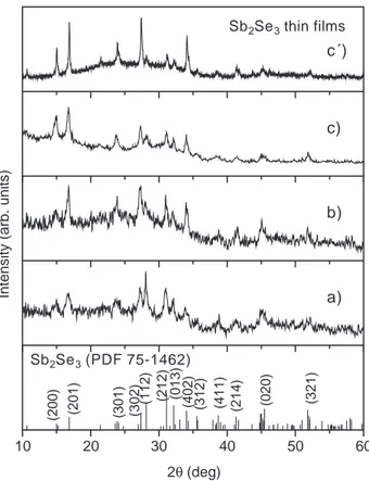
10 20 30 40 50 60
a) b)
Sb2Se3 (PDF 75-1462)
Intensity (arb. units)
2θ (deg)
c) Sb2Se3 thin films
(321)
(020)
(214)
(411)
(312)
(402)
(013)
(212)
(112)
(302)
(301)
(201)
(200)
c´)
process, films obtained from the three baths were heated at 573 K for 1800 s in Se-vapor evolved from 5 mg (6.3310 5 mol) of Se-powder placed along with the samples under a nitrogen pressure of 2000 mTorr. To make an upper estimate of the selenium requirement one can
assume a film thickness of 0.4Am for Sb2O3(formula mass,
291.5 g/mol; mass density, 5.84 g/cm3) and its conversion to Sb2Se3. Se-vapor of about 0.2410 5mol cm 2would be
required over the thin film surface, which is available from the Se-source utilized.
The XRD patterns of the films obtained from the three baths and heated in the presence of the Se-vapor are given in
Fig. 2. All the peaks in the patterns match well those reported for Sb2Se3 in PDF 75-1462. The peaks due to
Sb2O3,seen inFig. 1, are absent in the patterns. It was seen
in the composition analyses that the Sb : Se mole ratio approach 1 : 1.5 in the three cases. Scherrer formula may be utilized to estimate the average crystalline grain size. The values estimated for the different peaks are in the 15 – 30 nm range. It was observed that if 50 mg of Se-powder is utilized during the heating at 573 K for 1800 s, the XRD patterns become well defined, as illustrated in the XRD pattern cV) in
Fig. 2 for the film obtained from bath c). The crystalline grain diameter, evaluated from the peak at 2h= 16.87- due to diffraction from (120) planes, is about 30 nm.
3.2. Optical and electrical properties
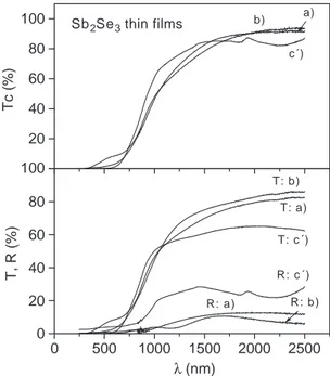
The optical transmittanceT(%) and specular reflectance
R (%) spectra of the films, of approximately 0.4 Am in thickness obtained from baths a) and b) heated in presence of 5 mg of selenium and that from bath c) as given in the XRD pattern cV) are given inFig. 3. The transmittance data were corrected assuming reflection loss at the air – film
0 500 1000 1500 2000 2500
0 20 40 60 80 100 20 40 60 80 100
R: c´)
R: a) R: b) T: c´)
T: a) T: b)
T, R (%)
λ (nm) Sb2Se3 thin films
c´) a) b)
Tc (%)
Fig. 3. Optical transmittance, reflectance, and transmittance corrected for reflectance loss (Tcorr) of the Sb2Se3films of labels a), b) and cV) described inFig. 2.
1.0 1.5
0 1 2 3 4
0.8 1.2 1.6
0 1 2 3 4
1.0 1.5 2.0
0 1 2 3 4 5 Sb2Se3
thin film s a)
1.11 1.19
(
α
h
ν
)
1/2
(10
2 cm
-1/2
eV
1/2
)
b)
1.22 1.02
hν (eV)
1.21
1.32 c´)
interface, Tcorr (%) = 100 T (%) / [100 R (%)] and are in Fig. 3asT(%). The slow decrease of the transmittance with decrease in wavelength is characteristic of indirect band gap. The optical absorption coefficients (a) at different wavelengths were calculated using the formulaa= (1 /d) ln 100 /Tcorr(%). InFig. 4, values of (ahm)2are plotted against
photon energy (hm) for the three cases of films. Straight line regions are observed over the photon energy range 1 – 1.7 eV. The smaller value indicated for the intercept in each case is the band gap energy minus the phonon energy and the larger, the sum of the two. Possible distribution of the crystalline grain diameter does not permit the exact evaluation of the band gap in thin films, but a value for the band gap in the 1.0 – 1.2 eV range appears to be a reasonable estimate for the crystalline Sb2Se3 thin films.
The reported value for the optical band gap of crystalline Sb2Se3is about 1.1 eV[1].
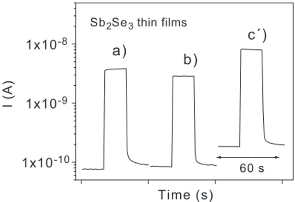
Fig. 5shows the photocurrent response of the crystalline Sb2Se3 films, obtained from the three different baths and
heated in presence of selenium, the XRD patterns and optical transmittance of which were given inFigs. 2 and 3 -a), b), and cV). A bias, 100 V has been applied in each case. The electrical conductivity of the films in the dark is in the range of (2 – 4)10 8 (V cm) 1, and upon illumination, there is an increase in the conductivity by more than an order of magnitude. The highest dark conductivity, 410 8 (Vcm) 1, and photoconductivity, 210 6(Vcm) 1, are observed in the case of the Sb2Se3thin film obtained from
bath c) and heated at 573 K in Se vapor.
In order to evaluate the product of mobility (l) and free carrier life-time (s) of photo generated charge carriers, photocurrent response for the film cV) was recorded with monochromatic radiation of 636.5 nm, obtained using an Oriel interference filter. The intensity of the radiation was 37 W m 2, as measured by an Eppley pyranometer. Thus, the incident photon density was 1.21020 photons m 2s 1.Fig. 3shows that at the wavelength used, 96% of the radiation is absorbed in the thin film. Considering the film thickness, 0.4 Am, an estimated value for the rate of optical absorption in the bulk of the film is, 51026 m 3 s 1. The increase in
conductivity upon illumination, 3.210 7 (V cm) 1, is,
Dr=qGls, and hence an estimate for the mobility – lifetime product (ls) is: 3.710 9 cm2 V 1. The best values for single crystal Si are around 1 cm 2V 1, with a carrier life time of about 1 ms and electron mobility, 103 cm2 V 1s 1. However, in polycrystalline thin films both these parameters are many orders of magnitude lower, arising from mobility lowering due to inter-grain electric potential due to oxygen chemisorption and life time reduction due to additional recombination processes at the film surface and intergrain region. Thus, the value of the mobility – lifetime product obtained in the present case is realistic. The value may be improved further through heat treatment designed for that purpose.
4. Conclusions
Thin films deposited from chemical baths constituted from antimony salts and sodium selenosulfate have been found to be containing crystalline oxide phase, Sb2O3, along
with antimony selenide, the presence of which cannot be clearly detected in XRD patterns, even after heating at 573 K in a nitrogen atmosphere. Composition analysis has suggested that the oxide phase might constitute half or more of the material of the thin film. Heating the films at 573 K in the presence of Se, evolved from Se-powder, transforms the entire film into Sb2Se3. These films show an indirect band
gap of 1 – 1.2 eV. The films are photosensitive. An estimate for the mobility – lifetime product of the polycrystalline Sb2Se3thin film is, 3.710 9cm2V 1.
Acknowledgements
The authors are grateful to Ma. Luisa Ramon and Leticia Ban˜os for recording the XRD patterns and to DGAPA-UNAM and CONACYT-Me´xico for the financial support awarded for this work.
References
[1] O. Madelung, Semiconductors other than Group IV elements and III – V compounds, in: R. Poerschke (Editor – in – Chief), Data in Science and Technology, Springer, Berlin, 1992, p.50.
[2] R.S. Mane, C.D. Lokhande, Mater. Chem. Phys. 65 (2000) 1. [3] P.K. Nair, M.T.S. Nair, V.M. Garcı´a, O.L. Arenas, Y. Pen˜a, A. Castillo,
I.T. Ayala, O. GomezDaza, A. Sa´nchez, J. Campos, H. Hu, R. Sua´rez, M.E. Rinco´n, Sol. Energy Mater. Sol. Cells 52 (1998) 313. [4] R.N. Bhattacharya, P. Pramanik, Sol. Energy Mater. 6 (1982) 317. [5] H.T. El-Shair, A.M. Ibrahim, E. Abd El-Wahabb, M.A. Afity, F. Abd
El-Salam, Vacuum 42 (1991) 911.
[6] K.Y. Rajpure, C.H. Bhosale, Mater. Chem. Phys. 62 (2000) 169. [7] A.P. Torane, K.Y. Rajpure, C.H. Bhosale, Mater. Chem. Phys. 61
(1999) 219.
[8] P. Pramanik, R.N. Bhattacharya, J. Solid State Chem. 44 (1982) 425. [9] V.M. Garcı´a, M.T.S. Nair, P.K. Nair, R.A. Zingaro, Semicond. Sci.
Technol. 12 (1997) 645. 1x10⁻¹⁰
1x10⁻⁹ 1x10⁻⁸
Sb2Se3 thin films
60 s c´) b)
a)
I (A)
Time (s)
Fig. 5. Photocurrent response of Sb2Se3thin films a), b) and cV) described in
[10] M. Moskovits, in: G. Soles (Ed.), Chemical Physics of Atomic and Molecular Clusters, North Holland, Amsterdam, 1990, p. 397. [11] Powder Diffraction File, Joint Committee on Powder Diffraction
Standards, International Center for Diffraction Data, Swarthmore, PA, Cards 43-1071 and 75-1462.