Semiconductor thin films by chemical bath
deposition for solar energy related applications
P.K. Nair
*
, M.T.S. Nair, V.M. Garcı´a, O.L. Arenas, Y. Pen
8
a,
A. Castillo, I.T. Ayala, O. Gomezdaza, A. Sa´nchez, J. Campos,
H. Hu, R. Sua´rez, M.E. Rinco´n
Department of Solar Energy Materials, Centro de Investigacio&n en Energı&a, Universidad Nacional Autonoma de
Me&xico, Temixco, Morelos 62580, Mexico
Received 1 October 1996; received in revised form 20 May 1997
Abstract
In this paper we present the basic concepts underlying the chemical bath deposition technique and the recipes developed in our laboratory during the past ten years for the deposition of good-quality thin films of CdS, CdSe, ZnS, ZnSe, PbS, SnS, Bi
2S3, Bi2Se3, Sb2S3,
CuS, CuSe, etc. Typical growth curves, and optical and electrical properties of these films are presented. The effect of annealing the films in air on their structure and composition and on the electrical properties is notable: CdS and ZnS films become conductive through a partial conver-sion to oxide phase; CdSe becomes photosensitive, SnS converts to SnO
2, etc. The use of
precipitates formed during deposition for screen printing and sintering, in polymer composites and as a source for vapor-phase deposition is presented. Some examples of the application of the films in solar energy related work are presented.(1998 Elsevier Science B.V. All rights reserved.
Keywords: Thin films; Growth curves; Optical and electrical properties
1. Introduction
Chemical bath deposition technique is well suited for producing large-area thin films for solar energy related applications. In this paper we would share our
*Corresponding author.
0927-0248/98/$19.00(1998 Elsevier Science B.V. All rights reserved
experience in this technique, acquired at the Laboratorio de Energia Solar (presently Centro de Investigacio´n en Energı´a) during the past 10 yr, with researchers in this field and others who would be interested to initiate work in this research area.
Chemical bath deposition is a technique in which thin semiconductor films are deposited on substrates immersed in dilute solutions containing metal ions and a source of hydroxide, sulfide or selenide ions. The earliest reported work dates back to 1919 and dealt with the deposition of PbS thin films [1]. The basic principles underlying the chemical bath deposition of semiconductor thin films and early research work in this area have been presented in a 1982 review article [2], which has inspired many researchers to initiate work in this area. The subsequent progress in this area is contained in a 1991 review article [3], which lists literature on more than 35 compounds prepared by this technique and related references. Recipes for the chemical bath deposition of a number of such compounds are given in a recent paper [4]. The number of possible materials to be produced through the technique is bound to multiply in subsequent years. This is due to the feasibility of producing multilayer films by this technique—the annealing of which promotes interfacial diffusion of metal ions and the production of new materials with improved thermal stabilities. For example, interfacial diffusions in chemically deposited PbS—CuS and ZnS—CuS coat-ings result in materials such as PbxCuySzand ZnxCuySzwith p-type conductivities and are stable up to a temperature of 300°C [5]. Annealing of Bi
2S3(bismuthinite)—CuS
(covellite) coating at temperatures of 250—300°C leads to the formation of a new compound, Cu
3BiS3(wittichenite), with p-type conductivity [6].
Among the first applications of chemically deposited semiconductor thin films, we find PbS and PbSe photodetectors [7]. Even though chemically deposited CdS films were developed during 1960s, the photodetector applications of CdS were confined to screen-printed and sintered layers [8]. However, chemically deposited CdSe thin films were found appropriate for photodetector applications [9]. In the late 1970s and early 1980s the motivation in the work on chemically deposited thin films has been their prospective solar energy applications. One of the earlier developments toward this was in solar absorber coatings [10], followed by specific application of such coatings in evacuated all-glass tubular collectors [11]. Application of the chemically deposited films in solar control coatings was suggested in 1989 [12]. Subsequently the perfor-mance evaluation of such coatings was reported [13].
The use of chemically deposited semiconductor films to develop photo-electrochemical solar cells was of basic interest, most importantly, in the case of CdS and CdSe thin films [2,14,15]. Recent work on chemically deposited CdSe and Sb
2S3
films with an incorporated WO
3component has shown improved conversion
efficien-cies and stabilities in photoelectrochemical solar cell configuration [16].
The integration of chemically deposited semiconductor thin films in thin-film solar cell has only a short history. In 1990, a thin layer of chemically deposited CdS thin film was integrated into a structure Mo—CuInSe
2—CdS—ZnO producing approximately
11% of conversion efficiency [17]. This was followed by improved cell design resulting in record efficiencies of'17% [18], in which the chemically deposited CdS film of
&0.05lm continued to play the role of an inevitable component. The incorporation
identified in 1979—80 as an essential step towards improving the solar cell stability [19]. Theoretical calculations done in 1982 [20] predicted that the thickness of the CdS film should be as small as possible to increase the cell efficiency. The chemical deposition technique, which excels in providing complete surface coverage at very small film thicknesses was therefore chosen to produce this very thin film with excellent success [21].
The use of chemically deposited n-CdSe or n-Sb2S3films with incorporated WO3 phase as an active absorber material in Schottky barrier solar cells has been proven factible. For example,»
0#of 0.72 V;I4#of 14.1 mA cm~2; FF of 0.7 and conversion
efficiency of 5.5% have been demonstrated in ITO-(n)CdSe(5lm)-Pt/Ni/Au(130 A_) Schottky cells [16,22,23]. Similarly, the fabrication of heterojunction solar cells using chemically deposited Sb
2S3thin films on (p)Si/(p)Ge/(p)InP wafers has been
demon-strated [16,22,24].
The photoaccelerated chemical deposition on PbS thin films was reported in 1991 [25] in which the illuminated region in a growing thin film showed accelerated deposition. The application of this effect in producing images in PbS thin film [26] and Bi
2S3thin film [27] has been reported. The potential use of the photoacceleration
effect in attaining high deposition rate is evident.
The above range of prospective applications, particularly, in the area of solar energy conversion and energy efficiency has prompted renewed interest in chemically deposited semiconductor thin films. The technique is ideally suited for the production of large area thin films as required for solar energy applications. In this paper we shall outline the technique for the preparation of a number of chemically deposited semiconductor thin films. The importance of post-deposition treatment in the modifi-cation of chemically deposited thin films for various applimodifi-cations and the prospects for producing new solar energy materials through interfacial diffusion of metal ions will be discussed. The use of the precipitate produced in the deposition bath during thin-film deposition, for the production of semiconductor coatings by other deposition techniques will also be presented.
2. Experimental
2.1. Chemical bath deposition
In the above-mentioned event, if the precipitation is controlled through the use of suitable complexing agents such as triethanolamine for the metal ions (so as to reduce the amount of free metal ions [30]) and the amount of sulfide, selenide, or hydroxo ions in the bath is controlled through setting up of appropriate chemical equilibria [2,3], thin-film deposition can take place. A further condition to be satisfied is the availability of nucleation centers over the substrate. Such centers are normally formed through the adsorption of metal hydroxo species over the surface. The hydroxo group would be substituted by the sulfide or selenide ions which would thereby form an initial layer of the metal chalcogenide [31]. The deposition of the thin film takes place through the condensation of the metal and sulfide/selenide ions on this initial layer, which acts as a catalytic surface.
The following compositions for the chemical deposition baths have been developed in our laboratory over many years. They have been tested for their reproducibility and have been found to be very reliable for the deposition of thin films in the thickness range 0.05—0.5lm. The given volumes of the constituents are the quantities required to prepare 100 ml of the deposition bath. The usual substrates are microscope glass slides, 75 mm]25 mm]1mm, cleaned in a detergent solution and rinsed well in running tap water. These are mounted nearly vertical on the wall of a 100 ml beaker containing the bath. Up to six substrates may be placed in a 100 ml beaker in this way. Deposition on a large-area commercial sheet glass may be made by slowly laying them down on a shallow tray containing the deposition bath. The sheet glass would be separated from the bottom of the tray by spacers in such a way that an approximately 5 mm thick layer of deposition bath separates the bottom surface of the sheet glass and the bottom of the tray. The thin-film deposition would take place at the bottom surface of the sheet glass. Coatings on sheet glass of 60 cm]60 cm are routinely made in our laboratory by this technique using approximately 2000 ml each of the depos-ition bath. Relatively low-cost reagents, of purity not more than 98%, are usually sufficient for the preparation of the deposition baths.
CdS thin film[32]: 30 ml of 0.1 M Cd(CH
3COO)2 ) 2H
2O, 8—12 ml of 1 M sodium
citrate, 15 ml of 1.5 M NH
4OH, 5—10 ml of 1 M thiourea, and the rest deionized water
to make the volume up to 100 ml. The deposition is allowed to proceed at 50—70°C for up to 12 h. Very smooth and uniform coatings of CdS are formed except at long durations of deposition.
CdSe thin films[33,34]: 30 ml of 0.1 M Cd(NO
3)2 ) 4H
2O, 12 ml of 1 M sodium
citrate, 1.2 ml of 30% (&15 M) NH
4OH, 0.4 g of N,N-dimethylselenourea dissolved
in 30 ml of freshly prepared 0.01 M Na
2SO3, and the volume made up to 100 ml with
water. Depositions may be made at room temperature (24 h) or at temperatures up to 60°C (8 h); at prolonged deposition there is risk of the film peeling from the glass substrates.
ZnS thin films[35]: 5 ml of 1 M zinc sulfate, 4.4 ml of NH
3/NH4Cl (pH 10), 5.4 ml of
50% triethanolamine, 2 ml of 1 M thioacetamide, and the rest deionized water to make up to 100 ml by volume. Depositions are made at 50°C for about 6 h or at room temperature for about 20 h to obtain ZnS films of 0.2lm thickness.
the volume made up to 100 ml with deionized water. Depositions may be made at room temperature or in an oven at temperatures up to 60°C.
SnS thin films[37]: 1 g SnCl
2 ) 2H
2O dissolved in 5 ml of acetone, 12 ml of 50%
triethanolamine, 8 ml of 1 M thioacetamide, 10 ml of 4 M NH4OH and the rest water to make up the volume to 100 ml. The depositions may be made at temperatures up to 80°C to obtain thin films of thickness 0.7lm.
PbS thin films[38]: 5 ml of 1 M Pb(CH3COO)2) 3H
2O, 20 ml of 1 M NaOH, 5 ml
of 1 M thiourea, 5 ml of 1 M triethanolamine, and the rest water. The quality of films is best when depositions are done at room temperature.
Bi
2S3thin films[39,40]: 10 ml ofK0.5 M Bi(NO
3)3 ) 5H
2O solution, 8 ml of 50%
triethanol-amine, 4 ml of 1 M thioacetamide, and the rest water. The depositions are made at room temperature; there is risk of peeling of the film from the substrate at intermediate durations (5—7 h), but are seen to be adherent when the films are allowed to remain in the bath for more than 24 h. Improved adhesion of the films are possible when the films are deposited over a substrate layer of ZnS [35].
Bi
2Se3 thin films [41]: 7 ml of 0.5 M Bi(NO3)3 solution, 7 ml of 50%
tri-ethanolamine, 20 ml of 0.07 M N,N-dimethylselenourea solution prepared freshly in 0.01 M Na2SO3, and the rest water. Films of 0.2lm may be deposited in about 9 h at 40°C or in about 60 h at room temperature. The films adhere well to glass substrates.
CuS thin films[42]: 5 ml of 1 M CuCl
2.3H2O, 4 ml triethanolamine, 8 ml of 30%
NH
4OH, 10 ml ofK1 M NaOH, 6 ml of 1 M thiourea, and the rest water. Depos-itions are made at room temperature for best results; the films peel from glass substrates during prolonged deposition, but it may be prevented by using a ZnS substrate film [35].
Cu
2~xSe thin films: 10 ml of 0.5 M CuSO4) 5H
2O solution, 1.5 ml of 30%
NH
4OH, 12 ml ofK0.4 M Na
2SeSO3solution (prepared by reflexing 4 g of selenium
powder in 100 ml of 1 M Na
2SO3solution for about 3 h), and the rest water. At room
temperature, films of approx. 0.2lm thickness are deposited in 7 h. The value of xmay depend on the exact bath composition and may even gradually change with the duration of deposition.
Sb2S3thin films: 0.65 g SbCl3dissolved in 2.5 ml of acetone, 25 ml of 1 M sodium thiosulfate, and the rest water to make up the volume to 100 ml. The depositions were done at 10°C in a refrigerator.
The compositions of deposition baths for many other compound semiconductor thin films developed in other laboratories are summarized in Ref. [3].
2.2. Characterization
3. Results and discussion
3.1. Growth of thinfilms
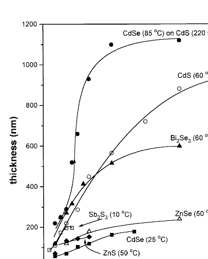
In general, the growth of good-quality semiconductor thin films by the chemical bath deposition technique proceeds at a slow pace. The technique is ideally suited for producing uniform films with thickness in the 0.05—0.3lm range in most cases. Film thickness up to a micron is possible in some cases. Thickness up to a few micron in chemically deposited CdSe and Sb
2S3 thin films have been reported from other
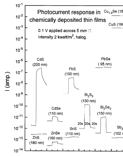
[image:6.466.100.307.291.549.2]laboratories [16]. Higher deposition rates and higher film thicknesses are usually accompanied by powdery deposits and a lack of specular reflection. Fig. 1 shows a few examples of the films deposited in our laboratory. All the films shown in the figure are specularly reflective. The bath compositions are stated in Section 2.1.
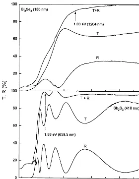
Fig. 2 illustrates the quality of the films: the transmittance,¹(j)%, and the specular reflectance,R(k)%, add up to nearly 100 at wavelengths longer than the threshold for optical absorption across the band gap. Arrows in the figure indicate the values listed for the optical band gap 1.03 eV (1204 nm) and 1.88 eV (659.5 nm) for Bi
2Se3and
Sb2S3, respectively [41,43].
Fig. 2. The near-normal reflectance (R%) and transmittance (T%) curves of Sb
2S3and Bi2Se3thin films indicating the presence of interference peaks. The sum ofR(%)#¹(%) is nearly 100% at long wavelengths,
indicating that the films possess nearly smooth surfaces. Arrows indicate the positions of absorption edges reported in Refs. [41,43].
3.2. Quantum confinement effect
The effect of crystallite size on the optical band gap of semiconductor thin films has been discussed by many researchers [44]. It is known that for an electron in a quantum well of width ¸, the quantized energy levels E
n are given by [45]
E
n"12(h/2p)2p2n2(m
%)~1/¸2. The ground-state energy is given by E
1"12(h/2p)2
p2(m
%)~1/¸2, wherehis the Planck’s constant andm
%is the effective mass of electron.
In the case of a polycrystalline semiconductor with crystalline grain width ¸, this leads to an enhancement of bandgap, (E
semiconductor crystal [46]:
(E
')1#"(E
')"6-,#12(h/2p)2p2(m~1
% #m~1
) )/¸2!(1.8/e¸), wherem
)is the effective mass for hole and the last term represents the screening term
in a medium of permittivity e. (E
')1# approaches (E')"6-, for ¸'50 nm, but takes values considerably higher than the bulk value for ¸(5 nm. For example, in chemically deposited CdSe films with grain sizes(5 nm, optical band gap of up to 0.7 eV higher than the bulk value (of 1.74 eV) has been reported [47].
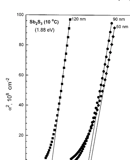
Fig. 3 illustrates this effect in the case of Sb
2S3thin films chemically deposited at
10°C. The plots of square of the optical absorption coefficient (a) versus the photon energy (hl) indicate direct band gaps for this film of about 0.7 eV higher than the bulk value (1.88 eV) for the band gap [43]. The grain size of these films are less than 5 nm; the X-ray diffraction patterns did not indicate any diffraction peak. These results for Sb2S3films are in agreement with those reported by other workers [48].
3.3. Preferential orientation of thefilms
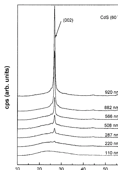
[image:8.466.99.310.300.559.2]Preferential orientation of the crystallites perpendicular to the plane of the sub-strate is a common feature observed in the case of chemically deposited CdS and CdSe
Fig. 3. The very small crystallites in chemically deposited thin films usually give rise to variation in band gaps due to quantum confinement effects; the case of Sb
Fig. 4. Preferential orientation of the crystalline grain, with thec-axis perpendicular to the plane of the substrates is observed in the case of chemically deposited thin films in the thickness range 110—920 nm.
thin films. Fig. 4 shows the typical case of CdS thin films deposited at 60°C, using citrate as a complexing agent as described in Section 2.1. The orientation is so pronounced that only the diffraction peak corresponding to the (0 0 2) planes is noticeable. The figure also shows that at very small film thicknesses the films appear to be amorphous or possess very small crystallites.
3.4. Photocurrent response
Fig. 5 shows the photocurrent response of a number of chemically deposited thin films. Except for CdS, the films do not exhibit large changes in the current upon illumination. Most films are highly resistive in the dark; the electrical conductivities in the dark range from 10~8to 10~6)~1cm~1. Exceptions are CuS and Cu
2~xSe thin
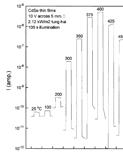
Fig. 7. Variation in the photosensitivity of the films produced by annealing of a CdSe film (&150 nm) in air
for 1 h each at different temperatures.
techniques as well [50]. The optical characteristics such as the one presented in Fig. 6 have been found to be ideal for application of these films in solar control glazing [51].
3.5. Effect of air annealing on the photo response curves
Air annealing leads to significant changes in the chemical, structural, electrical, and optical properties of chemically deposited semiconductor thin films. Notable exam-ples are the following:
CdSe thin films: The as-prepared thin films possess very poor photosensitivity:
S"(I
1)!I
$)/I$, whereI1)andI$are the photocurrent and dark current, respectively.
The CdSe thin films (&0.18lm thickness) in Fig. 7 were deposited at room temper-ature using N—N,dimethylselenourea as the source of selenide ions [33,34]. The photosensitivity increases from about 0.5 in as-deposited films to approximately 106 after the film has been annealed in air at 375—425°C for 1 h. This increase in
$&&&&&&&&&&&&&&&&&&&&&&&&&&&&&&&&&&&&&&&&&&&&
Fig. 6. Transmittance (¹%) and near-normal reflectance (R%) curves of chemically deposited CuS thin
films and Cu
xSe thin films, indicating the high near-infrared reflectance and low infrared transmittance
caused by the high electrical conductivities (&103)~1cm~1) of the films shown in Fig. 5. Arrows indicate
photosensitivity arises from the combined effect of grain size growth and chemisorp-tion of oxygen in the intergrain region as discussed in earlier papers [33,34]. The mechanism of enhancement of charge carrier mobility in polycrystalline thin-film semiconductors as a function of grain size and illumination have been the subject of many earlier studies [52,53]. In short, the chemisorbed oxygen at the intergrain region builds up repulsive potential for the transport of electrons, leading to very low electron drift mobilities and hence produces only very small electric currents. Illu-mination produces electron—hole pairs, of which the holes neutralize the repulsive potential at the grain boundaries and leads to an exponential increase in the electron mobility. This results in a high photocurrent under illumination which combined with the very low current in dark produces a high photosensitivity in the films.
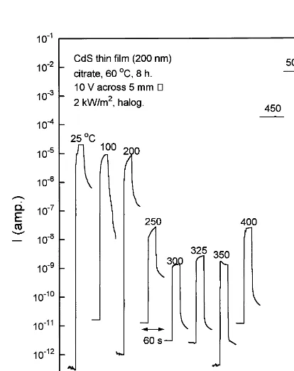
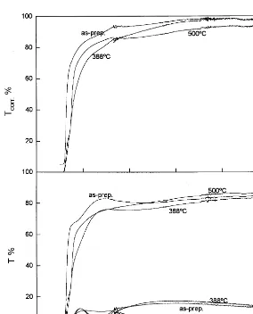
CdS thin films: In sharp contrast with the effect of air annealing on the photo-sensitivity of CdSe thin films, the photophoto-sensitivity of the CdS thin films degrades under the same annealing process. Fig. 8 shows that the photosensitivity of as-prepared films is nearly 108, but annealing at temperatures 300—400°C lowers it to 103—104. Annealing at higher temperatures improves the electrical conductivity drasti-cally, as reported previously [31]. The increase in conductivity arises from the formation of a top layer of CdO, which is highly n-type due to incomplete oxidation
Fig. 8. Effect of annealing in air for 1 h each at different temperatures of a CdS thin film (200 nm) on the photocurrent response curves; the high electrical conductivities (&50)~1cm~1) of the film obtained after
[image:12.466.102.309.287.548.2]which renders the CdO layer excess in Cd. X-ray photoelectron spectroscopy studies indicated that the CdO surface layer resulted from the CdS film [31], and the X-ray diffraction studies showed that the conversion could not be completed during the air annealing process—the presence of the underlying CdS film could be detected along with the CdO component. Assuming that the CdO film thickness is of about 100 nm (over the CdS film) in the case of the film annealed at 500°C in Fig. 8, the electrical conductivity is seen to be approximately 100)~1cm~1. Same range of conductivity is observed in CdO films produced by the oxidation of chemically deposited Cd(OH)
2
films [54]. Annealing the CdS films, prepared by the citrate method, in an inert atmosphere is yet to be studied. It may be possible to identify the optimum annealing conditions which would result in improvement in the grain size and hence enhance the photoconductivity in these films without decomposition to oxide.
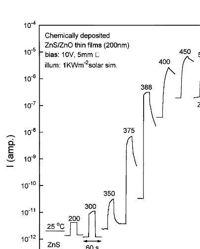
[image:13.466.104.306.291.542.2]ZnS thin films: Fig. 9 shows that the ZnS thin films of about 200 nm deposited at 25°C are very resistive; sheet resistance is of nearly 1012)/hand electrical conductiv-ity (dark/photo) is nearly 10~8)~1cm.~1Air annealing for 1 h at 388°C increases the photosensitivity toK104and annealing at 450°C for 1 h increases the photoconduc-tivity to'0.05)~1cm~1. The formation of a ZnO layer has been indicated by X-ray diffraction studies. The formation, however, is not complete. XRF studies have shown
the presence of about 30% of the initial sulfur content in the films after they were annealed at 450°C—500°C for up to 2 h. Thus, the ZnO is formed as a surface layer. The high conductivity arises from the incomplete oxidation, ZnO
1~x, similar to the
[image:14.466.61.345.190.542.2]case of CdO films. Fig. 10 shows that the ZnS—ZnO thin film maintains a high optical transmittance&80% in the near-infrared region and shows a shift in the optical band gap toward lower values. Thea2versushlplots for the film indicate band gap values of about 3.7 eV for the as-prepared and 3.4 eV for the ZnS—ZnO film produced by air annealing at 500°C for 1 h.
Fig. 10. The optical transmittance and reflectance spectra of a chemically deposited ZnS thin film, showing that the as-prepared and annealed (ZnS/ZnO) films possess high optical transmittance (¹
#033.%); ¹
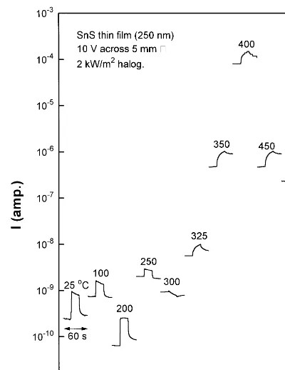
Fig. 11. Conversion of chemically deposited SnS thin films (250 nm) to SnO
2films (400—500°C) by air annealing.
SnS thin films: The as-prepared films in this case are very resistive. Annealing at about 300°C leads to the partial conversion of SnS to SnO
2~x; the nonstoichiometry
leads to high electrical conductivities. The proportion of SnO2~xin the film increases with temperature. Fig. 11 shows that at 400°C the conductivity of the film is the highest, about 0.5)~1cm~1. At this annealing temperature the SnS thin film, which originally appears orange-red in transmitted daylight becomes nearly transparent [55]. Annealing at temperatures above 400°C retains the film transparent, but leads to a better stoichiometry, SnO
2, which increases the resistance of the films.
3.6. Conversion of chemically depositedfilms to n-type by ion exchange reactions and diffusion of indium
In earlier papers we have discussed that immersion of CdS thin films in a dilute solution (0.05 M) of HgCl
2for a few minutes and annealing in air at 200°C for a few
Fig. 12. Conversion of chemically deposited CdSe thin films to n-type through deposition of a 20 nm indium film on the CdSe film (150 nm) and subjecting it to air annealing at 325°C for 1 h. A chemical etch for 6 h in a 1 M HCl solution removes the top In
2O3 layer, which exposes the underlying CdS : In layer.
well [56]. The increase in conductivity has been attributed to the incorporation of chlorine in the film. The drawback of this type of conversion to n-type is loss of the conductivity at higher annealing temperatures (300°C or above).
Recently, we reported another technique to convert the chemically deposited CdS [57,58] and CdSe thin films to n-type [59]. Fig. 12 illustrates the basic mechanism involved. A 20 nm thick indium film is evaporated over a chemically deposited CdSe thin film of about 150 nm thickness [59]. The quantity of indium required for this is about 15 mg to cover an area of 150 cm2 of the film surface. Annealing at 300—350°C produces an In
2O3 surface layer, which may
be removed by etching in 1 M HCl solution. The underlying film is indium-doped CdSe, i., CdSe : In. Fig. 13 shows that the conductivity of such a film is high: nearly 1)~1cm~1as compared to that of the CdSe film (10~7)~1cm~1) annealed in air under the same conditions. The conductivity was found to be stable during desiccated storage.
Fig. 13. Photocurrent response of annealed CdSe—In films, showing that a conductive In2O3 layer is formed on the film, which can be etched away in 1 M HCl solution. The underlying film after a 6 h etch is devoid of the In
2O3film (Fig. 12), but possesses a dark conductivity of 3)~1cm~1, nearly seven orders of magnitude higher than that of a CdSe film annealed under the same conditions.
precipitated in the medium, resulting from a reaction of the type
yPbS (crystalline)#xInPIn
xSy(amorphous)#yPb (crystalline).
This reaction takes place when the films are annealed at 300°C, and produces a composite material. The conductivity of this film is high: 500)~1cm~1and sheet resistance is about 100)~2.
3.7. Conversion of chemically deposited thinfilms to p-type by ion exchange reactions and interfacial diffusion
The conversion of chemically deposited CdS thin films to p-type by topotaxial reaction in a CuCl solution of pH 3.7 at 90°C for about 10 s has been developed as a method to produce CdS—Cu
2S solar cells in the 1980s [60]. The incorporation of
copper ions in chemically deposited CdSe thin films by immersion in a dilute solution of CuCl
2(0.005 M) has been reported before [56] from our group. The presence of
Cd
xCuySezcomposition in the surface layer, as evidenced in the XPS studies, gives rise
Fig. 14. XRD patterns illustrating that annealing in nitrogen of a PbS (200 nm)—In (20 nm) film results in the formation of metallic lead crystallites and the dispersion of indium in the matrix; the presence of which is detected in the X-ray flourescence spectra.
immersion for about 1 min of a ZnSe thin film in a 0.025 M CuCl
2solution reduces
the sheet resistance from about 1012)/h to 103)/h through the formation of a Zn
xCuySezcomposition on the surface layer [61].
Production of thermally stable thin films of p-type conductivity of about 300)~1cm~1 (sheet resistance of about 100)/h) is possible through interfacial diffusion of metal atoms in ZnS—CuS or PbS—CuS multilayers [5]. The films are stable in the temperature range 150—350°C under air annealing. More interesting results were obtained when Bi2S3—CuS films were annealed. The formation of a new com-pound Cu3BiS3(wittichenite) was suggested in a previous paper [62] and detailed results are presented in a recent paper [6]. Fig. 15 illustrates the mechanism of formation of the new film. Annealing the Bi
2S3—CuS films at temperatures of
200—300°C results in the interfacial diffusion of metal ions and formation of the new compound through the reaction
Bi
2S3#6CuSP2Cu
3BiS3#3S.
The excess sulfur may be removed by immersion in a suitable solvent. The conductiv-ity of the resulting film is '100)~1cm~1. This indicates that many chemically deposited thin films involving Cu
2~xSe, CuSe, CuS and CuxS may be subjected to
Fig. 15. The formation of a new material, Cu
3BiS3 (mineral sample; wittichenite) during annealing at 200—280°C of a chemically deposited Bi
2S3—CuS thin film (X-ray source, Cu Ka). 3.8. Use of the precipitate as a precursor for other coating techniques
The real challenge in the optimization of a chemical bath deposition technique is to reduce the particulate precipitate in the bath obtain in high thin-film yield. Neverthe-less, even in the best optimized bath, precipitate presents itself as a major product of the condensation process. The precipitate may be filtered and reacted with acids to produce the starting materials for deposition. But, in many cases the precipitate may be rinsed well, dried and stored to serve as precursor for other deposition techniques. Following are the three specific examples:
Fig. 16. X-ray (Cu Ka) diffraction pattern of a screen-printed and sintered (450°C) CdSe/ZnO layer prepared using CdSe precipitate and 30% by weight of ZnCl
2as flux (flux-to-pigment ratio, FPR"0.3)
dispersed in propylene glycol.
(anhydrous) and sufficient quantity of propylene glycol to produce a screen printing paste. The paste was screen printed on to glass substrates using a 120 T polyester screen (approx. mesh: sieve opening 44lm and filament diameter 30lm). The coating was dried in an air oven at 110°C for 1 h and sintered at 350—450°C in air for 1 h each. The XRD pattern in Fig. 16 for the coating sintered at 450°C shows well-defined peaks of CdSe and ZnO. A possible mechanism is that at temperatures above the melting point of ZnCl2, it melted and covered the CdSe pigment. At the sintering temperature ZnCl2combined with atmospheric oxygen forming ZnO. XRF studies have indicated that the chlorine content of the film has been significantly reduced in the sintered film—up to 10% of its original value in the dried screen printed coating. Fig. 17 illustrates the high photosensitivity achieved in the screen printed film prepared as above. The best photosensitivity, &108, is obtained for a sintering temperature of 450°C. Photosensitivity of even higher than this (for example, 109 under air mass one solar radiation) has been obtained in chemically deposited CdS thin films [66,67]. However, the fast decay of photocurrent of the screen printed CdSe/ZnO coatings is not matched by them.
Fig. 17. Photocurrent response (10 s dark, 10 s illumination, and 10 s dark) of the screen-printed CdSe/ZnO coating as a function of sintering temperature.
[image:21.466.120.290.341.554.2]Fig. 19. Variation of sheet resistance in CuS—poly acrylic acid composite coatings with temperature of annealing.
90 000), with propylene glycol used as a solvent. The conductivity percolation is seen at 40% w/w of CuS powder in the total weight of the composite. Sheet resistance of nearly 100)/h is obtained at a wt% of about 55% CuS. Higher wt% of the precipitate makes the surface of the coating rough. The results shown are for coatings annealed at 200°C. Fig. 19 shows that the conductivity does not degrade considerably when annealed at a temperature up to 250°C. Above this, there is chemical conversion of the CuS component to digenite, Cu
9S5, (JCPDS 26-0476) as illustrated in Fig. 20
and a transition of the coating to an insulator. The conversion may take place through the release of sulfur into the polymer matrix, for example, 15CuSP6CuS#Cu
9S5#4S. The resulting changes in chemical bonding have been studied by FTIR and discussed in Ref. [68].
Fig. 20. Partial conversion of the CuS (covellite) precipitate in the composite coatings to Cu
9S5(digenite) when the coatings are annealed at 300°C.
the temperature dropping to nearly 150°C at the far end. The geometry of the vapor phase deposition set up is discussed in Ref. [69].
Fig. 21 shows that the film deposited at a substrate temperature of 345°C during 5 h from the bismuth sulfide precipitate maintained at 500°C presents well-defined peaks. Even though there is a general agreement of the peak positions with that of standard Bi
2S3(bismuthinite, JCPDS 17320), the intensity ratios observed in the film vary from
that of the powder sample. This indicates preferential orientation of the crystallites. Fig. 22 shows the plot of the square of the product of the optical density (o.d)"(ad)/2.303 (whereais the absorption coefficient anddthe thickness of the film) and the photon energyE"hc/j(wherehis the Planck’s constant;cthe velocity of light; andjthe wavelength of radiation). The thin films possess a wide range of direct optical band gaps from 1.0 to 2.0 eV, depending on the temperature of the substrate. The range of photosensitivity,S"(I
1)!I
$)/I$"(p
1)!p
$)/p$(whereI1)andp1)are
the photocurrent and photoconductivity, respectively, and I$ and p$are the dark current and dark conductivity, respectively) varies widely as shown in Fig. 23. High electrical conductivity is typical of films deposited at higher substrate temperatures. Thus, the optical and electrical properties of the films may be varied depending on the chosen substrate temperature to suit specific applications of the films.
3.9. Chemically deposited semiconductor thinfilms for solar energy related applications
Fig. 21. XRD patterns of bismuth sulfide thin films deposited with substrate temperature of 345°C using bismuth sulfide precipitate as source, source temperature, 500°C at 4000 Pa. Standard patterns for Bi
Fig. 23. Photocurrent response of bismuth sulfide thin films deposited from vapor phase at different substrate temperatures using bismuth sulfide precipitate as the source. The values of photosensitivity
Sare given.
of the world; and (ii) it is available in a relatively dilute form, typically 20 MJm~2/day, as compared with nearly 30 MJ/kg obtainable from coal or petroleum. Collection of solar energy over a large area is inevitable. Chemical bath deposition is considered to be excellent in producing semiconductor thin films over large areas for such applications.
(i)Application in solar control coatings: In previous papers we have described the application of various chemically deposited semiconductor thin films for this purpose [12,13]. The basic purpose of this application is to reduce space cooling expenses in buildings and in automobiles by selectively controlling the amount of visible and infrared radiation entering through glazings. Chemically deposited CuS thin films have been found to possess near-ideal solar control characteristics: transmittance in the visible region of 20—50%, low transmittance, 10—20%, in the infrared region, low reflectance,(10%, in the visible region so as to avoid glare, and relatively higher reflectance,'15%, in the near-infrared region [70]. The coatings can be made on
$&&&&&&&&&&&&&&&&&&&&&&&&&&&&&&&&&&&&&&&&&&&&
sheet glass, acrylic, or polyester sheet and foils with equal ease [71]. To impart versatility and improvement of adhesion of the film to glass substrate, substrate films of chemically deposited PbS [72], SnS [73], ZnS [35], Bi
2S3[74], and ZnS—NiS [75]
have been proposed. A major problem in the application of these films was the need for a protective coating. The use of an aromatic polyurethene-based commercial transparent varnish was tried with limited success [76].
We have recently concluded that the best way to use chemically deposited solar control coatings is in the form of a laminated glazing. In this configuration, coatings were made on 3 mm thick commercial sheet glass and then laminated using a commercially available laminating polymer sheet of 0.4 mm thickness. This is a proprietary copolymer [77] of polyvinyl butyryl-acetate — alcohol with other ingredients added in order to prevent degradation of the polymer by the ultraviolet component of solar radiation. The lamination, of glass# coating— polymer—clear sheet glass, was done in an autoclave at 140°C under 2 kg cm~2 pressure for about 3 h.
Fig. 24 illustrates the transmittance and reflectance spectra of two different coatings CuS and PbS-CuS, where the individual coating thicknesses are of the order of 0.1lm. The spectra were recorded for incidence from the side of the coated glass — the recommended mode of incidence to minimize entry of the ultraviolet component of solar radiation into the polymer. The calculation of integrated reflectance (R) and transmittance (¹) in the visible (vis) and infrared (ir) were calculated for air mass two solar spectrum as described in Ref. [12]. The implication of these values in the solar control parameters of the glazing is discussed in Ref. [13]. The visible transmittance, ¹
7*4, of 51% and visible reflectance,R7*4, of 12% of the laminated CuS coatings are
suitable for use in automobile glazing and combination of¹
7*4"21%,R
7*4"18%,
and R
*3"28% of the laminated PbS—CuS coating are suitable for architectural
glazing applications.
(ii) Application as solar absorber coatings: Chemically deposited SnS—CuS [78], PbS—CuS and Bi
2S3—CuS [79] coatings have been investigated by us for application
Fig. 24. Optical transmittance and reflectance of CuS and PbS—CuS coatings deposited on 3 nm thick commercial window glass and laminated with a clear window glass (3 mm) using commercial-grade laminating polymer [77]. Laminating process: 140°C under 2 kg/cm2pressure for 2 h.
(iii) Photodetector and photovoltaic applications: Fig. 25 shows the dependence of the photoresponse curve of chemically deposited CdSe thin films as a function of the intensity of illumination. The dependence of the photocurrent on the intensity is nearly linear. The photo generation of such magnitude in the depletion layer of a Schottky barrier or p—n, p—i—n junction leads to the build up of photo voltage. We consider that the possibility of creating new materials through interfacial diffusion of atoms in chemically deposited multilayer stacks as demonstrated in PbS—CuS, ZnS—CuS and Bi
2S3—CuS films [5,6] is very high. Table 1 suggests a list of possible
Fig. 25. Photoresponse curves of a CdSe thin film annealed in air at 450°C at different illumination levels (0.01%), 0.2 W m~2 and to 100%, 2.12 kW m~2 illustrating near-linear dependence of photocarrier generation on the intensity of illumination—a basic feature on which photovoltaic effect depends.
Table 1
Suggestions for the development of new solar cell/solar energy materials which may be prepared through the interfacial diffusion of ions in multilayer chemically deposited thin films during annealing. The data have been extracted from Ref. [43]
Material Structure Band gap (eV) Hole mobility
(cm2/Vs) CuSbSe
2 Orthorhombic 0.83 5
AgSbS
2 Monocl. 1.73 1500
AgSbSe
2 Rock salt 0.58
AgBiS
2 Rock salt 0.9
Cu
3SbS4 Zincblende 0.46
Cu
3SbSe4 Zincblende 0.31 50
Ag
2SnSe3 0.81 910
Cu2SnSe3 0.96 870
Cu2SnS3 0.91 605
[image:28.466.26.385.424.564.2]Ref. [43], which may be produced by solid-state reaction of the type
2CuS#SnSPCu
2SnS3(E'"0.91 eV),
PbS#SnS
2PPbSnS
3(E'"1.05 eV),
Bi2S3#Ag
2SP2AgBiS
2(E'"0.9 eV),
Sb2S3#Ag
2SP2AgSbS
2(E'"1.73 eV),
etc., where the CuS [42], SnS [37], PbS [38], Bi
2S3[39] Ag2S [81] Sb2S3[48] films
are produced by chemical bath deposition. In the case of SnS and SnS
2, it has been
reported that by controlling the bath composition and temperature either of the composition may be obtained [82]. Further, new materials may also be created by combining chemical deposition technique with thermal evaporation or sputtering of metals, for example, Sb
2S3#3CuS#3CuP2Cu
3SbS3, etc. We consider that
cre-ation of new thin-film materials by the above approaches is vital for the further advancement of the chemical bath deposition technique and integration of the films produced in this way into solar energy technologies.
3.10. Toxicity considerations
The chemical deposition technique involves the use of dilute solutions of com-pounds involved in the reaction. This offers minimum toxicity and occupational hazards since the vapor phase of the reactants are avoided. It is well known that toxicity hazards associated with lead, cadmium, mercury, selenium, etc, are severe when inhaled [83]. An analysis on the toxicity hazard in the production of chemically deposited PbS thin films is given in Ref. [84] where it was established that the chemical bath technique does not entail the usual health hazards associated with lead pollution. Further, the unreacted ions can be precipitated in the bath as sulfides or selenides and the solid can be separated and stored for use as discussed above in Section 3.8 or recycled to produce starting material. The formation of multinary compounds by interfacial diffusion and recrystallization in multilayer films as given above can be considered as an environmentally sound process since very few effluents are produced. Overall, the-large area capability and the ease of scaling up with complete control of material handling in solid or liquid phase offers perspective toward the industrial production of coatings and devices by the chemical bath deposition technique.
4. Conclusions
Acknowledgements
The authors are grateful to Leticia Ban8os of the Instituto de Investigaciones en Materials, UNAM, for recording the XRD patterns. Financial support for this work was received from CONACYT, Me´xico through 1816-E9211 and from DGAPA-UNAM through IN-502594 and IN-501495. One of us (V.M.G) is grateful to the Universidad Autonoma de Zacatecas for financial support.
References
[1] O. Houser, E. Beisalski, Chem-Ztg. 34 (1910) 1079.
[2] K.L. Chopra, R.C. Kainthla, D.K. Pandya, A.P. Thakoor, in: G. Hass, M.H. Francombe, J.L. Vossen (Eds.), Physics of Thin Films, vol. 12, Academic Press, New York, 1982, p. 201.
[3] C.D. Lokhande, Mater. Chem. Phys. 27 (1991) 1—43. [4] I. Grozdanov, Semicond. Sci. Technol. 9 (1994) 1234.
[5] L. Huang, P.K. Nair, M.T.S. Nair, R.A. Zingaro, E.A. Meyers, J. Electrochem. Soc. 141 (1994) 2536. [6] P.K. Nair, L. Huang, M.T.S. Nair, Hailin Hu, E.A. Meyers, R.A. Zingaro, J. Mater. Res. 12, 1997,
(in Press).
[7] D.E. Bode, in: G. Hass, R.E. Thun (Eds.), Physics of Thin Films, vol. 3, Academic Press, New York, 1966, p. 275.
[8] A.G. Stanley, Cadmium Sulfide Solar Cells, in: R. Wolf (Ed.), Applied Solid State Sciences, vol. 5, Academic Press, New York, 1975, p. 251.
[9] S.V. Svechnikov, E.B. Kaganovich, Thin Solid Films 66 (1980) 41.
[10] G.B. Reddy, V. Dutta, D.K. Pandya, K. L Chopra, Sol. Energy Mater. 15 (1987) 383; 15 (1987) 153.
[11] C. Estrada-Gasca, G. Alvarez-Garcı´a, R.E. Cabanillas, P.K. Nair, Renewable Energy 2 (1992) 477; J. Phys. D 25 (1992) 1142.
[12] P.K. Nair, M.T.S. Nair, A. Ferna´ndez, M. Ocampo, J. Phys. D 22 (1989) 829. [13] C. Estrada-Gasca, G. Alvarez-Garcı´a, P.K. Nair, J. Phys. D 26 (1993) 1304. [14] R.A. Boudreau, R.D. Rauh, J. Elctrochem. Soc. 130 (1983) 513.
[15] M.E. Rinco´n, M. Sa´nchez, A. Olea, I. Ayala, P.K. Nair, Photoelectrochemical behavior of thin CdS, coupled CdS/CdSe semiconductor thin films, Solar Energy Mater. Solar Cells (1997), These pro-ceedings.
[16] O. Savadogo, Chemically and electrochemically deposited thin films for solar energy materials, Solar Energy Mater. Solar Cells (1997) These proceedings.
[17] Bluent Basol, Vijay Kapur, IEEE Trans. Electron Dev. 37 (1990) 418.
[18] T.R. Tuttle, M.A. Contreras, J.S. Ward, A.L. Tennant, K.R. Ramanathan, J. Keane, R. Noufi, in: C.M. Lampert et al. (Ed.), Proc. SPIE, vol. 2531, SPIE, Bellingham, 1995, p. 194.
[19] M.A. Mickelsen, W.S. Chen, Appl. Phys. Lett. 36 (1980) 371.
[20] A. Rothwarf, Proc. 16th IEEE Photovoltaic Specialists Conf., San Diego, CA, IEEE, New York, 1982, p. 791.
[21] B.M. Basol, V.K. Kapur, A. Halani, C. Leidholm, in: K.A. Summers (Ed.), Annual Report, Photovol-taic Subcontract Program FY 1991, Golden, NREL, p. 50.
[22] O. Savadogo, K.C. Mandal, Appl. Phys. Lett. 63 (1993) 12. [23] O. Savadogo, K.C. Mandal, J. Electrochem. Soc. 141 (1994) 2871. [24] O. Savodogo, K.C. Mandal, J. Phys. D 27 (1994) 1070.
[25] P.K. Nair, V.M. Garcı´a, A.B. Hernandez, M.T.S. Nair, J. Phys. D 24 (1991) 1466. [26] P.K. Nair, O. Gomezdaza, M.T.S. Nair, Adv. Mater. Opt. Electron. 1 (1992) 139.
[27] P.K. Nair, M.T.S. Nair, O. Gomezdaza, R.A. Zingaro, J. Electrochem. Soc. 140 (1993) 1085. [28] J. Basset, R.C. Denney, G.H. Jeffery, J. Mendham, in: Vogel’s Textbook of Quantitaive Inorganic
[29] D.R. Lide, (Editor-in-Chief), CRC Handbook of Chemistry and Physics 76th Ed., CRC Press, Boca Raton, 1995-96, pp. 8-58.
[30] J. Bjerrum, B.V. Agarwala, S. Refn., Acta Chem. Scand. A 35 (1981) 685. [31] N.R. Pavaskar, C.A. Menezes, A.B.P. Sinha, J. Electrochem. Soc. 124 (1977) 743. [32] M.T.S. Nair, P.K. Nair, R.A. Zingaro, E.A. Meyers, J. Appl. Phys. 75 (1994) 1557.
[33] M.T.S. Nair, P.K. Nair, H.M.K.K. Pathirana, R.A. Zingaro, E.A. Meyers, J. Electrochem. Soc. 140 (1993) 2987.
[34] V.M. Garcı´a, M.T.S. Nair, P.K. Nair, R.A. Zingaro, Semicond. Sci. Technol. 11 (1996) 427. [35] P.K. Nair, M.T.S. Nair, Semicond. Sci. Technol. 7 (1992) 239.
[36] C.A. Estrada, P.K. Nair, M.T.S. Nair, R.A. Zingaro, E.A. Meyers, J. Electrochem. Soc. 141 (1994) 802. [37] M.T.S. Nair, P.K. Nair, Semicond. Sci. Technol. 6 (1991) 132.
[38] P.K. Nair, M. Ocampo, A. Fernandez, M.T.S. Nair, Sol. Energy Mater. 20 (1990) 235; V.M. Garcı´a, M.T.S. Nair, P.K. Nair, Sol. Energy Mater. 23 (1991) 47.
[39] M.T.S. Nair, P.K. Nair, Semicond. Sci. Technol. 5 (1990) 1225.
[40] P.K. Nair, J. Campos, A. Sa´nchez, L. Ban8os, M.T.S. Nair, Semicond. Sci. Technol. 6 (1991) 393. [41] V.M. Garcı´a, M.T.S. Nair, P.K. Nair, R.A. Zingaro, Semicond. Sci. Technol. 12 (1997) (May issue), in
press.
[42] P.K. Nair, V.M. Garcı´a, A.M. Ferna´ndez, H.S. Ruiz, M.T.S. Nair, J. Phys. D 24 (1991) 441. [43] O. Madelung, in: Semiconductors other than Group IV elements, III—V compounds, Springer, Berlin,
1992.
[44] M. Moskovits, in: G. Soles (Ed.), Chemical Physics of Atomic and Molecular Clusters, North Holland, Amsterdam, 1990, p. 397.
[45] For example, M.N. Rudden, J. Wilson, Elements of Solid State Physics, Wiley, Chichester, 1980, p. 59. [46] L. Brus, J. Chem. Phys. 90 (1986) 2555.
[47] G. Hodes, A.A. Yaron, F. Decker, P. Motisuke, Phys. Rev. B 36 (1987) 4215. [48] K.C. Mandal, O. Savadogo, Sol. Energy Mater. Sol. Cells 26 (1992) 117.
[49] K. Okamoto, S. Kawai, Jpn. J. Appl. Phys. 12 (1973) 1130; J.J. Loferski, J. Schewchun, S.D. Mittleman, E.A. DeMeo, R. Arnott, H.L. Hwang, R. Beauliew, G. Chapman, Sol. Energy Mater. 1 (1979) 157. [50] H.S. Randhawa, R.F. Bunshah, D.G. Brock, B.M. Basol, O.M. Staffsudd, Sol. Energy Mater. 6 (1982)
445.
[51] M.T.S. Nair, P.K. Nair, Semicond. Sci. Technol. 4 (1989) 191.
[52] J.W. Orton, B.J. Goldsmith, J.A. Chapman, M.J. Powell, J. Appl. Phys. 53 (1982) 1602. [53] M.V. Garcı´a-Cuenca, J.L. Morenza, J.M. Cordina, J. Phys. D 20 (1987) 951.
[54] R.L. Call, N.K. Jaber, K. Seshan, J.R. Whyte, Sol. Energy Mater. 2 (1980) 373. [55] P.K. Nair, M.T.S. Nair, R.A. Zingaro, E.A. Meyers, Thin Solid Films 239 (1994) 85.
[56] M.T.S. Nair, P.K. Nair, H.M.K.K. Pathirana, R.A. Zingaro, E.A. Meyers, J. Electrochem. Soc. 140 (1993) 2987.
[57] P.J. George, A. Sa´nchez, P.K. Nair, M.T.S. Nair, Appl. Phys. Lett. 66 (1995) 3624. [58] P.J. George, A. Sa´nchez-Juarez, P.K. Nair, Semicond. Sci. Technol. 11 (1996) 1090. [59] V.M. Garcı´a, P.J. George, M.T.S. Nair, P.K. Nair, J. Electrochem. Soc. 143 (1996) 2892.
[60] M. Savelli, J. Bougnot, in: B.O. Seraphin (Ed.), Solar Energy Conversion and Topics in Applied Physics, vol. 31, Springer, Berlin, 1979, p. 213.
[61] C.A. Estrada, R.A. Zingaro, E.A. Meyers, P.K. Nair, M.T.S. Nair, Thin Solid Films 247 (1994) 208. [62] P.K. Nair, M.T.S. Nair, H.M.K.K. Pathirana, R.A. Zingaro, E.A. Meyers, J. Electrochem. Soc. 140
(1993) 754.
[63] K.L. Chopra, S.R. Das, in: Thin Film Solar Cells, Plenum, New York, 1982, p. 233.
[64] H. Matsumoto, K. Kuribayashi, H. Uda, Y. Komatsu, A. Nakamoto, S. Ikegami, Sol. Cells 11 (1984) 367.
[65] O. Gomezdaza, V.M. Garcı´a, M.T.S. Nair, P.K. Nair, Appl. Phys. Lett. 68 (1996) 1987—1989. [66] P.K. Nair, M.T.S. Nair, J. Campos, L.E. Sansores, Sol. Cells 22 (1987) 213.
[70] M.T.S. Nair, P.K. Nair, Semicond. Sci. Technol. 4 (1989) 599. [71] H. Hu, P.K. Nair, Surface Coating Technol. 81 (1996) 183. [72] P.K. Nair, M.T.S. Nair, Semicond. Sci. Technol. 4 (1989) 807. [73] M.T.S. Nair, P.K. Nair, J. Phys. D 24 (1991) 450.
[74] M.T.S. Nair, G. Alvarez-Garcia, C. Estrada-Gasca, P.K. Nair, J. Electrochem. Soc. 140 (1993) 212. [75] A.M. Fernandez, M.T.S. Nair, P.K. Nair, Mater. Manufr. Process 8 (1993) 535.
[76] A.M. Fernandez, P.K. Nair, Thin Solid Films 204 (1991) 459.
[77] Vitro Vidrio Plano-Industria Quimica M, S.A. de C.V., Tlaxcala-Puebla, Tlaxcala C.P.90780 AP 942 Me´xico.
[78] P.K. Nair, M.T.S. Nair, J. Phys. D 24 (1991) 83.
[79] V.M. Garcia, M.T.S. Nair, P.K. Nair, Solar Energy Mater. 23 (1991) 47. [80] B. Window, Solar Energy 31 (1983) 159.
[81] A.J. Varkey, Solar Energy Mater. 21 (1991) 291.
[82] R.D. Engelken, H.E. McCloud, C. Lee, M. Slayton, A. Ghreishi, J. Electrochem. Soc. 134 (1987) 2696. [83] N.I. Sax, Dangerous properties of Industrial Materials, 6th ed., Van Nostrand, Reinhold, New York,
1984, p. 612, 1693, 1751, 2390.