DOI 10.1007/s10948-010-0811-z O R I G I N A L PA P E R
Study of Vacancies and Pd Atom Decoration on the Electronic
Properties of Bilayer Graphene
D.H. Galvan·A. Posada Amarillas·
R. Núñez-González·S. Mejía·M. José-Yacamán
Received: 7 April 2010 / Accepted: 18 June 2010 / Published online: 21 July 2010 © Springer Science+Business Media, LLC 2010
Abstract We have investigated the scenario of graphene when irradiated with high energetic protons and subse-quently decorated with Pd atoms on one of the layers. The-oretical analyses were performed on graphene 2L (two lay-ers) with vacancies (carbon 3 and 13) (sample A), graphene 2L with vacancies and the two carbon atoms intercalated in between the two carbon layers (sample B), graphene 2L with the vacancies intercalated and subsequently with two Pd atoms on one of the layers, the top layer (called surface) (sample C), and, last but not least, graphene 2L with vacan-cies intercalated and decorated with six Pd atoms on the sur-face (sample D). For the four cases enunciated, energy bands were performed which provided information about the semi-metallic behavior, showing more semi-semi-metallic character for the first case, while less metallic behavior occurs for the
D.H. Galvan (
)Centro de Nanociencias y Nanotecnología, Universidad Nacional Autónoma de México, Apartado Postal 2681, C.P. 22800, Ensenada, B.C., Mexico
e-mail:[email protected] A. Posada Amarillas
Departamento de Investigación en Física, Universidad de Sonora, Apartado Postal 5-088, C.P. 83190, Hermosillo, Sonora, Mexico R. Núñez-González
Departamento de Matemáticas, Universidad de Sonora, C.P. 8300, Hermosillo, Sonora, Mexico
S. Mejía
Facultad de Ciencias Físico-Matemáticas, Universidad Autónoma de Nuevo León, San Nicolas de los Garza, Nuevo León, C.P. 66451, México
M. José-Yacamán
Department of Physics and Astronomy, University of Texas at San Antonio, San Antonio, TX 78249, USA
second and third one. Moreover, sample D showed a mini gap (between the conduction and valence bands) of the or-der of 0.02 eV and manifest semiconductor behavior. Total and projected density of states were performed in order to provide information about the contributions from each se-lected atom to the total DOS in the vicinity of the Fermi level in order to analyze the effect on the electronic behav-ior. Pd d orbitals contribute with ∼6% to the total DOS, while graphene (carbon atoms) p orbitals contribute with ∼5%. Furthermore, a strong hybridization is manifest be-tween these two multiple degenerate orbitals.
In addition, Crystal Orbital Overlap Population (COOP) between metal (M–M) contributions were calculated in or-der to inquire the existence (or absence) of magnetic insta-bilities. Pd atoms showed an itinerant ferromagnetic behav-ior which induces it to the graphene 2L samples.
Keywords Graphene·Tight-bind·Energy bands·Density of states·Crystal orbital overlap population
1 Introduction
The study of radiation damage was extensive in the past because of the interest in fission reactors. Recently, a re-newed interest in radiation damage studies has been driven by the need to expand new sources of energy and avoid en-vironmental effects of hydrocarbons. Indeed, the ment of advanced nuclear reactors is linked to the develop-ment of materials capable to operate under higher irradiation fluxes [1–6].
Graphite, a two-dimensional allotrope of carbon on a honeycomb lattice, has been used extensively as a basis for the discussion of carbon nanotubes [9]. Moreover, graphene is characterized by Dirac electrons [7] which is a 2D zero-gap semiconductor with very interesting electronic proper-ties.
Graphene showed unusual properties derived from its re-duced dimensionality as well as its small size, which yielded an enormous potential for use in ultra-fast electronic transis-tors and switches.
In this work, we proceed as a continuation of a study per-formed in our group [10] when graphene was irradiated with a high energetic proton beam. In this case, the irradiated graphene was decorated with Pd atoms in order to investi-gate their effect on the electronic and magnetic properties.
It has been shown before [11–13], that irradiation of HOPG (Highly Oriented Pyrolitic Graphite), using a high flux electron beam, produces breaking of the basal plane, disordering and even some tilt in the sample as well as cre-ation of vacancies in different areas. In this case the main radiation damage is produced by the electron beam.
2 Theoretical Calculations
The calculations were carried out by means of the tight-binding method [14] within the extended Hückel [15] frame-work using YAeHMOP computer package [16, 17]. It is good to stress that the extended Hückel method is a semi-empirical approach for solving the Schrödinger equation for a system of electrons, based on the variational theorem. In this approach, explicit electron correlation is not considered except for the intrinsic contributions included in the parame-ter set for each atom in question and which were obtained from S. Alvarez et al. [18] or from the most accurate ab initio calculations. The calculations were performed in the supercomputer Altix 350 located in Mexico City, and using the input files according to each specific case (Table1).
Table 1 Atomic parameters used in the extended Hückel tight-binding calculations,Hii(eV) andς(valence orbital ionization potential and exponent of Slater-type orbitals). The d orbitals for Pd are given as a linear combination of two Slater-type orbitals. Each exponent is fol-lowed by a weighting coefficient. A modified Wolfsberg–Helmholtz formula was used to calculateHij[28]
Atom Orbital Hii ςi1 C1 ςi2 C2
C 2s −21.4 1.62
2p −11.40 1.62 0.0000 0.0000 0.0000
Pd 5s −7.32 2.19
5p −3.75 2.15
4d −12.02 5.98 0.5535 2.613 0.6701
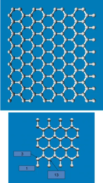
Fig. 1 (a) Super cell generated from an infinite single sheet of car-bon atoms which arose from crystalline graphite. (b) A graphite single sheet made of 40 carbon atoms is depicted. Notice that carbons 3 and 13 were removed in order to create the vacancies. Then a duplication of a single sheet is used in order to create the AA configuration
These calculations were performed on a system selected as a repeated cluster originated from a super cell. The super cell was generated from an infinite single sheet of carbon atoms, as depicted in Fig.1(a), which arose from crystalline graphite using the following primitive vectors:a=2.456 Å,
c=6.696 Å, space group 194 [19].
The density of vacancies is of the order of∼2.5% with re-spect to the total of atoms in the unit cell. Moreover, these two carbon atoms were displaced from the original location and then located at a distance of 1.67 Å (half way between the two layers) from the top layer following an intercala-tion between the two sheets. The second layer was created by a duplication of the 40 carbon atoms sheet (with no va-cancies) in the AA configuration. The former configuration was made with the purpose of simulating a real scenario if graphene 2L were subjected to proton irradiation.
A natural candidate to generate magnetism in coated graphene is Pd, due to its very polarizable bands. Further-more, Pd is not intrinsically magnetic due to its close shell configuration ([Kr]364d10) of the d orbitals. Although, in bulk, the s and d bands of Pd hybridize and exhibit Pauli paramagnetism with a high density of states in the vicinity of the Fermi level.
With these considerations in mind, our goal is to con-sider two layer (2L) graphene with two vacancies (carbon 3 and 13) intercalated in between the two layers and decorated with Pd atoms on one of the layers, in order to inquire the changes occurring in the electronic and magnetic properties due to the addition of Pd atoms.
3 Results and Discussion
3.1 Band Structure Calculations
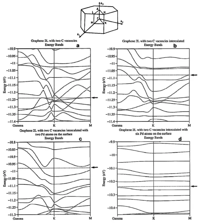
Band structure calculations for samples A to D are depicted on Figs.2(a) through2(d) respectively. The inset in Fig.2 depicts the Wigner–Seitz cell for a hexagonal configuration used in the band structure calculations. The Fermi level is in-dicated by a horizontal dotted line and inin-dicated by a small arrow, separating the valence band (VB) from the conduc-tion band (CB). Energy in eV vs.k-values (in the reciprocal space) were plotted for each case, ranging fromΓ (0 0 0)to M(1/2 0 0)to K(1/3 1/3 0)of(4/√3)∗(π/a).
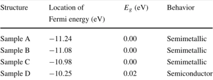
Table2provides information regarding the location of the Fermi level (eV), value of the forbidden energy gapEg(eV), and electronic behavior of the different scenarios under in-vestigation. For each figure the vertical axis is the total en-ergy in eV vs.kpoints in reciprocal space (horizontal axis). Figure2(a) provides information regarding energy bands for sample A. Notice that a set of multiple degenerate bands cross the Fermi level, which is located at−11.24 eV. Obvi-ous to say, that the system presents a semi-metallic behav-ior. Figure2(b) yields energy bands for sample B. The two carbon atoms were displaced from its original location and were placed at 1.64 Å from the lower layer. Notice some dif-ferences were encountered when compared with Fig. 2(a). The Fermi level was shifted to−11.08 eV with respect to the lower level. Moreover, the system behaves as less semi-metallic due to only two degenerate bands being interlaced
and crossing the Fermi level. The difference could be at-tributed to the interaction of the two carbon atoms with the two carbon sheets and then displaced form the network and intercalated in between the two layers.
In addition, Fig.2(c) yields information regarding sam-ple C. Separation in between two Pd atoms is of the order of 2.84 Å (in the same plane) and these two atoms were lo-cated at 0.98 Å (perpendicular) from the surface. Note that the Fermi level has been displaced to−10.98 eV. Further-more, the system continues to present a semi-metallic be-havior like case B. The difference encountered could be at-tributed to the interaction of the two Pd atoms with them-selves and then with one of the carbon layers. Moreover, Fig.2(d) corresponds to sample D. The differences encoun-tered with respect to sample A are the following. The Fermi level was displaced to−10.25 eV while a mini gap (between the valence and conduction bands) was manifest. The mini gap was of the order of∼0.02 eV, indicating that the system behaves like a small gap semiconductor. This result implies that the 6 Pd atoms strongly influence the system, changing from semi-metallic to semiconductor behavior.
Performing an analysis to the slopes of the curves cross-ing the Fermi level, it is possible to see that in Figs.2(a) to2(d), two curves cross the Fermi level indicating the semi-metallic behavior. Moreover, the slope of each figure is neg-ative and increases going from sample A to D. On the other hand, Fig.2(d), sample D, none of the curves crosses the Fermi level, providing an indication of semiconductor be-havior, whereas the slope of one of the curves in the vicin-ity of the Fermi level is negative and bigger than the slopes of the curves from samples A to C. A conclusion could be drawn from this analysis: while the slope of the curves in-creases, the semi-metallic behavior decreases until the sys-tem becomes a semiconductor.
In addition, we considering the concept of the effective massm∗:
1/m∗=−2d2E(k)/dk2. (1)
Here=h/2π, the reduced value, whileh=6.626×10⁻²⁷ erg-sec is the Planck constant. It is necessary to stress that
d2E(k)/dk2 is related to the concavity of each curve
un-der consiun-deration. Henceforth, notice that the concavity in-creases for samples A to D, implying thatm∗decreases in that order.
Fig. 2 (a) Band plots for sample A. Notice that the Fermi level crosses two multiple degenerate bands, providing the semi-metallic behavior The inset depicts the Wigner–Seitz cell for a hexagonal configuration. (b) Band plots for sample B. Notice that two multiple degenerate bands cross the Fermi level, providing the semi-metallic behavior. (c) Band plots for sample C. Two multiple degenerate bands cross the Fermi
level. Notice that the slope of the curves crossing the Fermi level are bigger than those from sample A. This fact yields an indication that the system is less metallic. (d) Band plots for sample D. Notice that there is no crossing of bands of the Fermi level. A mini gap of the order of
∼0.02 eV between the conduction and valence bands is manifested
network; the one remaining is apz in the perpendicular di-rection of the hexagon which is free to interact with orbitals belonging to foreign atoms. As explained before, Pd d and s orbitals hybridize between themselves. Once the Pd (two or six atoms) is located in the center of each hexagon of the car-bon network, we see interaction with thepzorbitals forming
a new hybridization which provides the final behavior of the sample in question.
Table 2 Location of the Fermi level (eV), value forEg(eV) and elec-tronic behavior for different configurations of graphene
Structure Location of Eg(eV) Behavior Fermi energy (eV)
Sample A −11.24 0.00 Semimetallic
Sample B −11.08 0.00 Semimetallic
Sample C −10.98 0.00 Semimetallic
Sample D −10.25 0.02 Semiconductor
addition of carbon and Pd atoms to create samples A to D make the Fermi level shift up or down in energy according to the specific case in question. From the energy band analysis it was not possible to identify which set of bands contribute most to the total DOS, nor which atoms are for the most responsible for this effect; henceforth, total and projected DOS in the vicinity of the Fermi level was performed.
3.2 Total and Projected DOS
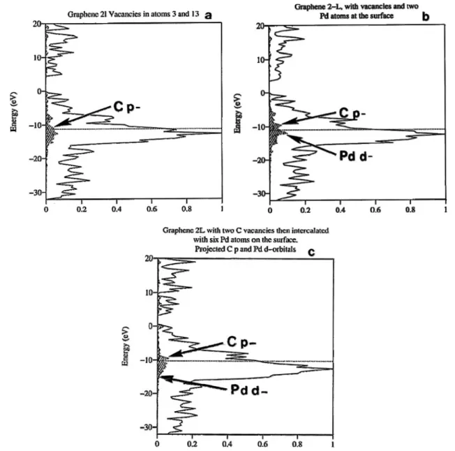
Total and projected DOS for samples B, C and D are de-picted in Figs.3(a) to3(c). Solid lines in the figures repre-sent the total DOS, while dotted and shaded lines reprerepre-sent the projected orbitals from the selected atoms in question. A horizontal dotted line indicates where the Fermi level is located. The vertical axis corresponds to energy (eV) while the horizontal axis corresponds to the % contribution to the total DOS. It is necessary to stress that in each graph the highest peak is selected as 100% contribution and all other peaks are rescaled with respect to it. In order to make the analysis simpler, only a finite number of carbon atoms were selected and projected. If all the carbon contributions were added together, the total DOS will be reproduced com-pletely. Afterwards, only the projection of specific orbitals from the atoms that contribute most to the total DOS located in the vicinity ofEf were selected, because the electric and magnetic properties are made manifest by those contribu-tions.
Figure3(a) yields the total and projected DOS obtained for sample B. Notice that graphene p orbitals contribute with ∼6% to the total DOS. On the other hand, Fig.3(b) corre-sponds to sample C. Comparing this result with the results obtained for sample A, some differences were encountered, especially on the shape of the total DOS. Likewise, graphene p orbitals and Pd d orbitals were projected to see the inter-action between these orbitals. Graphene p orbitals contribute ∼6% while Pd d orbitals with the same symmetry contribute with∼5% to the total DOS. Most of all, a clear hybridiza-tion (overlap) between these orbitals is manifest.
On the other hand, Fig. 3(c) corresponds to sample D. Again, some differences were encountered when compar-ing to sample B. Graphene p orbitals contribute with∼6%
while Pd d orbitals contribute with∼1%. Also, notice that the Fermi level crosses a valley in the DOS manifesting a mini gap of the order of∼0.02 eV. Unfortunately the mini gap is so small that it appears as a continuous line in the total DOS.
A very important question regarding the opening of a mini gap, case D, should be addressed. As we explained before, when a single sheet of carbon atoms is created,pz orbitals from each carbon atom point up or down. Thesepz orbitals interact with the orbitals of the same symmetry, of the two carbon atoms that were intercalated. These interac-tions are severe enough so as to induce instabilities in the system, in such a way as to enhance the possibility of open-ing mini gaps in certain high symmetry points in the First Brillouin Zone (FBZ). Moreover, when Pd atoms (two or six) are placed on the top layer, more interactions are cre-ated between the Pd and thepz orbitals from each carbon that form the honeycomb network. All of these interactions enhance the probability for the appearance of mini gaps in certain points in the FBZ.
3.3 Crystal Orbital Overlap Population
Another objective of this study is to find a correlation be-tween the occurrence (or absence) of a ferromagnetic transi-tion in terms of chemical bonding. A technique has been de-veloped by Landrum et al. [20]. They showed that the pres-ence of M–M (M=metal) antibonding states at the Fermi level serves as a finger print to indicate the possibility for the existence of ferromagnetic instabilities.
Crystal Orbital Hamiltonian population (COHP) analy-sis [23] is a partitioning of the band structure energy in terms of orbital-pair contributions. The COHP provides a quanti-tative measure of bond strength and is appropriate for a first-principle calculation.
Landrum et al. [20] showed that using the concept of Crystal Orbital Hamiltonian Population (COHP) is equiv-alent to the use of the Crystal Orbital Overlap Population (COOP) technique used when extended Hückel theory is performed. COOP provides the total overlap population, which is not identical to the bond order, but scales like it [22]. Positive regions refer to bonding, while negative re-gions indicate antibonding. The amplitude of the curves de-pends on the number of states in that specific interval, the magnitude of the coupling overlap, and the size of the co-efficients in the molecular orbital under consideration. An-other simpler way to explain COOP is as follows: COOP could be understood as the orbitals (from each atom that form the solid) working together to make bonds in the crys-tal.
Fig. 3 (a) Total (solid line) and projected (hatched line) DOS for sample B. Indicated with an arrow is the contribution from carbon p orbitals. (b) Total (solid line) and projected (hatched line) for sample C. Indicated with arrows are carbon p and Pd d orbitals. A careful analysis has been performed for those contributions in the vicinity of
the Fermi level. (c) Total (solid line) and projected (hatched line) for sample D. Indicated with arrows are carbon p and Pd d orbitals. Notice that the Fermi level falls in a valley of the DOS. An energy gap of the order of∼0.02 eV is obtained
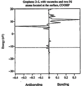
highest peak on the graph is considered 100%. Again, the Fermi level is indicated by a horizontal dotted line. From Fig. 4, notice that the Fermi level crosses a region of an-tibonding M–M contribution. As a result, there exists a driving force which induces the creation of ferromagnetism in the compound. The method used in the calculation did not include spins (α(up) andβ (down)) effects, from a formal point of view. It is necessary to underline the following: fer-romagnetism is a chemical phenomenon arising only in sys-tems with a critical electron concentration, one which causes the Fermi level to fall in a region of antibonding states. The resulting instability originates with lowering of the original
symmetry. Moreover, Landrum et al. [20] demonstrated that a driven force for the creation of ferromagnetism was the re-moval of M–M antibonding states from the vicinity ofEF as a result of the exchange splitting. The exchange splitting as well as the differential spatial extent of the two spin sub-lattices arises because of differential shielding ofα andβ
electrons.
Fig. 4 COOP for sample C. Notice that the Fermi level falls in a region with antibonding behavior, yielding information on the existence of a ferromagnetic instability
be expected as the result of the hybridization of the bands as predicted by Chen et al. [25]
On the other hand, graphene is more electronegative than Pd, hence carbon π bands are shifted up in energy. In the cases under consideration, Pd d orbitals hybridize strongly with graphene pz orbitals but the Stoner condition [26, 27] is not satisfied, henceforth the system does not magne-tize until a local interaction parameter is considered mak-ing Pd bands strongly polarized and a total magnetization is observed in the Pd unit cell indicating a ferromagnetic in-stability producing a strong itinerant magnetism in coated graphene.
4 Conclusions
From the calculations described herein, the following con-clusions about graphene decorated with Pd atoms can be drawn. The calculated energy bands for samples A, B and C showed semi-metallic behavior, while for sample D they yielded a small gap semiconductor.
From total and projected DOS, it was possible to identify the contribution from each orbital of each atom in the cases enunciated in the former paragraph. Afterwards, a careful analysis of the main contributions to the total DOS in the vicinity ofEf indicates that a strong hybridization occurred between Pd d orbitals with graphenepzorbitals as was pre-dicted by Chen et al. [25]
Nevertheless, COOP on graphene 2L (c) provides evi-dence of the existence of itinerant ferromagnetism induced into the graphene layers.
Acknowledgements D.H.G. acknowledges Prof. R. Escudero for providing the subject for investigation. The authors would like to acknowledge Y. Flores and the people from Supercomputo-DGSCA UNAM for their technical support. D.H.G. acknowledges E. Aparicio, J. Peralta and M. Sainz for assistance in the preparation of this manu-script. This work was supported by grants of NSF and the Welch foun-dation. The work is part of ICNAM Program at the University of Texas and CONACYT.
Appendix A
The Extended Hückel Molecular Orbital calculation (EHMO) is the simplest approximation Linear Combina-tion of Atomic Orbitals Molecular Orbital (LCAO-MO) ap-proximation (2). The cij are called the molecular orbital coefficients. They may be either positive or negative and the magnitude of the coefficient is related to the weight of that AO in the MO. EHT uses only the valence orbitals of each atom in the molecule or solid, namely one s and three p orbitals for main elements, plus five d orbitals for the tran-sition elements. These AO are assumed to be real functions and normalized such that the probability of finding an elec-tron in øi when integrated in all space is unity (2a). The MOs are normalized and orthogonal (i.e. orthonormal) (2b).
α=
cαøj, α=MO(α), øj=AO(j ) (2)
øi|øi =
ø∗iøidτ=1 (2a)
α|β =
α∗βdτ=δαβ (2b)
in bracket notation.
In the eigenvalue equation (3) the energyεαmeasures the effective potential exerted on an electron located in theαth molecular orbital (MO)α .
Hα=εαα (3)
εα= α|H|α (3a)
The coefficients are chosen such that the energy is mini-mized (3a).
The system of linear equations obtained is express in a compact form in (4). The theory of simultaneous equations requires that the determinant (5) vanishes.
[Hij−εαSij]cij=0 (4)
|Hij−εαSij| =0 (5)
To solve (4) the EHMO method introduces some assump-tions.
of the isolated atom in the appropriate state (Valence State Ionization Potential).
Hii= −VSIP(øj) (6)
This value can be derived from spectroscopy or com-puted from accurate methods (ab initio).
(ii) The off-diagonal elements of H are evaluated accord-ing to the Wolfsberg–Helmholtz relation (6) whereK
is an adjustable parameter.
Hij=KSij(Hii+Hij)/2 (7)
(iii) Basis set: the atomic valence orbitals are approximated with Slater-type orbitals (STO), of single type for s
andp, double zeta ford orbitals:
øs,p=rn−le(−ς r)Y (θ, ω) (8)
ød=rn−l[C1e(−ς1r)+C2e(−ς2r)]]Y (θ, ω) (9)
wheren=principal quantum number;r=distance of the electron from the nucleus;Y (θ, ω)=angular part of the wavefunction; ς, ς1, ς2, C1,C2 are tabulated computer constants.
References
1. Banhart, F.: Rep. Prog. Phys. 62, 1181 (1999)
2. Ajayan, P.M., Ebbesen, T.: Rep. Prog. Phys. 60, 1025 (1997) 3. Banhart, F., Füller, T., Redlich, Ph., Ajayan, P.M.: Chem. Phys.
Lett. 269, 349 (1997)
4. Thrower, P.A., Mayer, R.M.: Phys. Status Solidi A 47, 11 (1978) 5. Burden, P.A., Hutchison, J.L.: J. Cryst. Growth 158, 185 (1996) 6. Koike, J., Pedraza, D.F.: J. Mater. Res. 9, 1899 (1994)
7. Novoselov, K.S., Geim, A.K., Morozov, S.V., Jiang, D., Zhang, Y., Dubonos, S.V., Grigorieva, I.V., Firsov, A.A.: Science 306, 666 (2004)
8. Novoselov, K.S., Geim, A.K., Morozov, S.V., Jiang, D., Katsnel-son, I.V., Grigorieva, I.V., Dubonos, S.V., Firsov, A.A.: Nature 438, 197 (2005)
9. Saito, R., Dresselhaus, G., Dresselhaus, M.S.: Physical Properties of Carbon Nanotubes. Imperial College Press, London (1998) 10. Galvan, D.H., Posada-Amarillas, A., Mejia, S., Wing, C.,
José-Yacamán, M.: Fullerene, Nanotub. Carbon Nanostruct. 18, 1 (2010)
11. Berger, C., Song, Z., Li, X., Wu, X., Brown, N., Naud, C., Mayou, D., Li, T., Hass, J., Marchenkov, A.N., Conrad, E.H., First, P.N., de Heer, W.A.: Science 312, 1191 (2006)
12. Burden, P.A., Hutchison, J.L.: Carbon 35, 567 (1997) 13. Banhart, F.: J. Appl. Phys. 81, 3440 (1997)
14. Whangbo, M.-H., Hoffmann, R.: J. Am. Chem. Soc. 100, 6093 (1978)
15. Hoffmann, R.: J. Chem. Phys. 39, 1397 (1963)
16. Landrum, G.A.: The YAeHMOP package is freely available at: http://overlap.chem.Cornell.edu:8080/yaehmop.html. F orbitals are included in the calculations as version 3.0×, using W.V. Glassey’s routine
17. Glassey, W.V., Papoian, G.A., Hoffmann, R.: J. Chem. Phys. 111, 893 (1999)
18. Alvarez, S.: Tables of Parameters for Extended Hückel Calcula-tions. Universitat de Barcelona, Barcelona (1993)
19. Hoffmann, U., Wilm, D.Z.: Elektrochem. 42, 42 (1936)
20. Landrum, G.A., Dronskowski, R.: Angew. Chem. Int. Ed. 1560, 39 (2000)
21. Castro-Neto, A.H.: Nat. Mater. 6, 176 (2007)
22. Hoffmann, R.: Solids and Surfaces: A Chemist’s View of Bonding in Extended Structure, VCH, New York (1988)
23. Dronskowski, R., Blöchl, P.E.: J. Phys. Chem. 97, 8617 (1993) 24. Egelhoff, W.F., Tibbetts, G.G.: Phys. Rev. B 19, 5028 (1979) 25. Chen, L.S., Wu, R.Q., Kioussis, N., Blanco, J.R.: J. Appl. Phys.
81, 4161 (1997)
26. White, R.M.: Quantum Theory of Magnetism, McGraw-Hill, New York (1970)