Mechanisms driving the catastrophic optical damage in high power
laser diodes
J.Souto
1, J.L.Pura
1, M.Rodríguez
1, J.Anaya
2, A.Torres
1, J.Jiménez*
11
GdS Optronlab, Universidad de Valladolid, Ed. i+d, Paseo de Belén, 1, 47011 Valladolid, Spain
2CDTR, H.H.Wills Laboratory, University of Bristol, BS81TL Bristol, UK
ABSTRACT
The catastrophic optical damage (COD) of laser diodes consists of the sudden drop off of the optical power. COD is generally associated with a thermal runaway mechanism in which the active zone of the laser is molten in a positive feedback process. The full sequence of the degradation follows different phases: in the first phase, a weak zone of the laser is incubated and the temperature is locally increased there; when a critical temperature is reached the thermal runaway process takes place. Usually, the positive feedback leading to COD is circumscribed to the sequential enhancement of the optical absorption in a process driven by the increase of the temperature. However, the meaning of the critical temperature has not been unambiguously established. Herein, we will discuss about the critical temperature, and the physical mechanisms involved in this process. The influence of the progressive deterioration of the thermal conductivity of the laser structure as a result of the degradation during the laser operation will be addressed.
Keywords: Laser diodes, degradation, thermal conductivity, thermal stresses
1. INTRODUCTION
Because of the demand of increasing optical power from laser diodes, reliability remains to be a strong challenge for the use of these devices in many applications. The understanding of the degradation mechanisms of high power laser diodes is critical to improve their power and lifetime. The failure of the laser diodes is due to the generation of extended defects in the active parts of the laser structure during the laser operation1,2; in high power laser diodes the thermal management
is a critical issue because of the important amounts of wasted power in a small volume. Degradation of laser diodes during operation constitutes a serious drawback for both laser manufacturers and end users. Extended defects in the quantum well (QW), waveguide and claddings resulting from the fabrication process are responsible for infant mortality, known as the rapid degradation mode. However, the generation of extended defects during operation is difficult to screen, and it leads to the catastrophic optical damage (COD), a harmful degradation event, since it takes place without previous warning. The COD consists of the sudden drop off of the optical power. COD involves a thermal runaway mechanism in which the active zone of the laser can reach very high temperatures, ending by melting3.
The extended defects are formed because of the atomic bond breaking, which evidences that the yield strength of the active materials is reached during the laser operation. Hence, stresses have to be produced, which should be responsible for the generation and subsequent propagation of networks of dislocations. Degraded devices present dark line defects (DLDs), which are regions of the active zone of the laser with very low or null light emission. The DLDs are locally generated, either at the front facet, or inside the cavity; then they propagate along the cavity driven by the optical field4,5. The physical
mechanism leading to the formation of such lines and the associated loss of output optical power is described in the literature5, but there is not a consensus about the origin of the COD, and about the technological factors that can strengthen
the laser diodes. Usually, the COD is described in a sequence of different processes, in the first step the process is incubated, this step is certainly related to the long term degradation1,6, in which point defects are generated in a slow process. The
local accumulation of these defects will form “weak” zones in the active region. These “weak” zones react to the laser field leading to the COD process. In fact, the “weak” zones are defect rich zones, which when interacting with the electric current and/or laser light can trigger the catastrophic degradation. In the presence of defects an initial temperature increase can occur, obeying to different physical mechanisms, e.g. non radiative recombination at defects, or local Joule heating due to local resistance changes; note that the presence of defects can contribute to both mechanisms.
Thickness (µm) Doping x% A1xGa1_xAs
150 CuW heat sink
3.000 AuSii soldering
0.120 P 0
0.050 P 55->0
0.890 P 55
0.080 P 65->55
0.500 P 65
0.130 P 26->65
0.012 10
0.130 N 65->26
0.500 N 65
0.080 N 55->65
1.000 N 55
1.500 N 0->55
ilk
130 N 0
When the “weak” region accumulates sufficient energy it reaches a critical temperature, for which a sudden increase of the optical absorption takes place, resulting in the thermal flash that has been observed by means of a thermocamera in lasers operating in pulsed mode5,7. This COD triggering has been reported to occur for facet temperatures between 120ºC and
200ºC, depending on the laser structure and the nature of the active region. This is the so-called critical temperature for COD4,7-9.
One needs to understand how such a temperature is reached at certain regions of the laser active zone, and why the critical temperature constitutes a turning point for the optical absorption of the laser light. Once the critical temperature is reached the DLDs propagate very fast (microseconds scale); on the other hand, the propagation is driven by the laser field as it propagates along the waveguide, for both broad and narrow emitters. Furthermore, the damage is mainly concentrated in the QW, which is destroyed, but it can also touch the guide layers. We present here an analysis of the critical temperature in QW laser diodes using finite element methods for solving the heat transport equation in a laser diode structure.
2. LASER STRUCTURE
The studied devices are broad area AlGaAs/GaAs graded-index separate-confinement heterostructures (GRINSCH) that emit at 808 nm. The core of the device consists of a 12 nm QW layer of Al0.10Ga0.90As sandwiched in between two 130 nm
barrier layers with graded aluminium concentration growing from 0.26 to 0.65 as the distance from that central layer increases. The main parameters used for the calculations were taken from the literature10. The complete multilayer structure
is schematically shown in Table 1. A more detailed description of the lasers is given in previous works10,11.
Table 1. Laser diode structure.
3. THERMOMECHANICAL MODELING
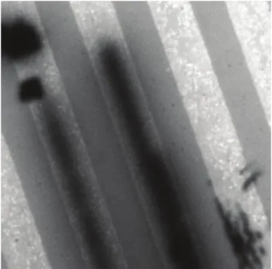
The COD process can be subdivided in two consecutive steps. First a critical temperature is reached; once this situation is met, a sharp temperature increase is produced in a process fed by the thermal bandgap shrinkage with the concomitant laser light absorption, leading to temperatures close to the melting point. During this step the defects grow very quickly forming extended motifs, with the corresponding laser output power drop. These defects are revealed by cathodoluminiscence (CL) imaging and they normally give a true dark contrast11, which permits to distinguish them from
other defects, which though giving dark contrast are still able to emit light (Fig.1).
In previous works, we have developed a thermo-mechanical model for studying the role of local heating on high power lasers10,12,13. This model, which can be applied to different laser structures, relies on the assumption that the origin of the
13316 13318 13320 133 22 133.24 133 26 z (isn)
follow. Alternatively, one can consider that the point defects might induce local electricalresistance changes, which would enhance the temperature by local Joule heating. The origin of the local temperature increase is out of the present scope, though it is a very relevant point to consider in forthcoming analyses.
In our model, the heat transport from this local heat source in the laser multilayer structure is solved by finite element methods (fem). Thereafter, one resolves the thermo-mechanical equation resulting from the local stresses induced by the previously determined temperature gradients in a structure formed by layers with different properties, both thermal and mechanical.
Figure 1. CL image of the QW emission showing fully dark lines along the ridges.
A key factor for these studies is the evaluation of the thermal conductivity suppresion associated with the nanoscale dimension of the QW14,15. We have followed the analytical model proposed by Liang and Li14 in order to include the
relevant surface scattering and size confinement effects. This model is in line with experimental studies of thermal conductivity on AlAs/GaAs superlattices (SL)16-19. In particular, the application of this model to the available data leads to
estimated interface roughnesses raging from ~2.5-5 Å, that correlate well with the expected 1-2 monolayer thickness for the transition layer in high-quality SLs20. These values for the roughnesses will therefore be chosen as the initial parameters
for the QW in the laser prior to the degradation. The additional suppression of the thermal conductivity due to disorder and dislocations generated during the laser operation within the active region21,22 will have to be considered when the
degradation of the device sets in. The effect of the disorder within the layer will be tackled in this model by considering increased roughness, as that change in the roughness parameters would also lead to poorer thermal conductivity.
Figure 2. Temperature profile across the laser structure for a heat source of 6 MW in the mirror facet, for three different interface roughness (2.5 Å, 7.5 Å and 10 Å), showing the peak temperature in the QW, and the lower temperature in the guiding layers.
(guides and claddings). This inhomogeneous temperature distribution is the consequence of the differences in the thermal conductivity of the different layers constituting the laser structure, and the thermal barriers at the interfaces, and of the suppression of the thermal conductivity associated with the nanoscale dimension of the QW14,15. In this calculation, the
dependence of the thermal conductivity and other physical parameters with T was explicitly considered.
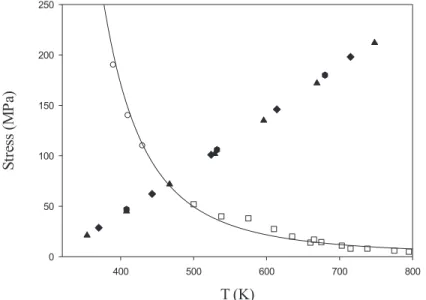
In the frame of our thermo-mechanical model the critical temperature is the temperature at which the QW generates dislocations due to the thermal stresses induced by the local heating. This has been discussed in previous articles10,12,13,
and the results are summarized in Fig. 3, where one represents the shear stresses for different values of the maximum T (temperature of the heat source in the QW), for a range of heat powers and various properties of the laser structures. The results are roughly aligned along a line that crosses the bulk GaAs yield strength vs T plot. As depicted in Fig. 3, the crosshatch occurs at about 480 K, which suggests that around this temperature, at which the yield strength is reached, the dislocations start to form under the mechanical stresses induced by the local heating. Therefore, in a first approach this can be considered to be the critical temperature.
T (K)
400 500 600 700 800
St
re
ss (
M
P
a)
0 50 100 150 200 250
Figure 3. Shear stress vs QW temperature for different laser power densities and different interface roughnesses. The open circles and squares represent the experimentally determined yield strength of bulk GaAs. The filled symbols correspond to the computed temperature-Tresca stress values for 2.5 Å (triangles), 7.5 Å (diamonds) and 10 Å (hexagons) roughnesses. The intersection between the calculated temperature-stress data and the measured yield strength of bulk GaAs represens the onset of plasticity, which occurs somewhat below 500K for the different scenarios represented.
4. DISCUSSION
The critical temperature has been experimentally measured with different techniques, as microRaman spectroscopy, thermo-reflectance, micro-photoluminescence, thermal imaging by using a thermocamera… If the first method is considered, measuring the temperature in a laser under operation uses large probes (ϕ≥1μm), and so the estimated temperature should be an average over a region at least two orders of magnitude larger than the QW thickness, where the highest temperature is reached. Hence, one can argue that those measurements are severely underestimating the peak temperature reached in the QW. Furthermore, in micro-Raman measurements the Raman signal arising from the QW is not observed because of the very small scattering volume. Therefore, the temperature measurement in the front facet of the laser corresponds to the temperature of the guides and claddings averaged over the probe beam23.
2 4 6 8 10 12 14
Power (MW /cm2)
2 4 6 8 10 12 14
Power (MW /cm2)
600
500
H
400
300
ái
2 4 6
Power (MW /cm2)
8 10 1','
the QW, Fig.4b. The measurements with the thermocamera give higher temperature than the spectroscopic techniques24,25,
because of the T4 law dependence of the radiation, which enhances the weight of the emission from the hottest region, the
QW, with respect to the other layers. Fig. 4c shows the temperature averaged over the thermocamera pixel size making use of the T4 emission law and the average temperature distribution derived from the temperature distribution calculated by
finite elements. In any case, the experimentally measured critical temperature is well below the peak temperature in the QW. This has consequences on the interpretation of the the critical temperature, as well as on our current understanding of the COD mechanisms.
Figure 4. a) Average temperature estimated from the calculated temperature distribution, when an optical probe (e.g.Raman) is used for temperature measurements. b) Peak temperature calculated at the QW. c) The same as (a) but using the T4 law,
which reproduces with more fidelity the thermocamera measurements. The data are obtained for different interface roughness, for increasing the interface roughness the thermal conductivity across the laser structure is decreased. Note the important discrepancies between the three graphs for the same laser power density and the same interface roughness.
According to the initial estimation described in Fig.3, the onset for the plastic deformation occurs for a temperature of ~480K, which is not too far from the critical temperatures reported in the literature. However, in our calculations this is the peak temperature (QW temperature), while the measured average temperatures correspond to the adjacent guides. Assuming peak temperatures of around 500K, the temperature of the adjacent layers is too low to match the experimental critical temperature. This suggests the need to revise the criteria followed to define the critical temperature. In previous papers we have estimated the starting of the COD when the shear thermal stresses overpass the yield strength of bulk GaAs. However, this approach is probably not fully correct, if one considers the hardening due to the reduced dimensions of the QW26, which will displace the onset of plasticity to significantly higher stresses. Furthermore, this criterion could
still be too conservative, if one considers that a strong optical absorption is necessary to increase the local temperature at the QW to values that would correlate to those experimentally measured. Therefore, a sufficient volume of dislocations would be required to absorb that substantial part of the optical power. As the number of dislocations grows, the laser absorption would increase accordingly, and so would the temperature at the QW. This suggests that the critical temperature would be reached well after the mechanical flow regime starts.
5. CONCLUSIONS
ACKNOWLEDGEMENTS
This work was funded by the Spanish Government (Grant: MAT2010-20441-C02-01-02) and Junta de Castilla y León (VA293U13).
REFERENCES
[1] Waters, R.G. “Diode laser degradation mechanisms: a review”, Prog. Quantum Electron. 15, 153-174 (1991).
[2] Tomm, J. W. and Jiménez J., [Quantum Well Laser Array Packaging], MacGraw-Hill, New York (2006).
[3] Henry, C. H., Petroff, P. M, Logan, R.A. and Merritt, F. R. “Catastrophic damage of AlGaAs double-heterostructure material”, J. Appl. Phys. 50, 3721-3732 (1979).
[4] Hempel, M., La Mattina, F., Tomm, J. W., Zeimer, U., Broennimann, R. and Elsaesser, T. “Defect evolution during catastrophic optical damage of diode lasers”, Semicond. Sci. Technol. 26, 075020 (2011)
[5] Nakwaski, W. “Thermal analysis of the catastrophic mirror damage in laser diodes”, J. Appl. Phys. 57, 2424-2430 (1985).
[6] Jiménez, J. “Laser diode reliability: crystal defects and degradation modes”, Comptes Rendus Physique 4, 663-673 (2003)
[7] Tomm, J. W., Ziegler, M., Hempel, M. and Elsaesser, T. “Mechanisms and fast kinetics of the catastrophic optical damage (COD) in GaAs-based diode lasers”, Laser and Photonics Reviews 5, 422-441 (2011).
[8] Moser, A. and Latta, E.E.,“Arrhenius parameters for the rate process leading to catastrophic damage of AlGaAs- GaAs laser diodes”, J. Appl. Phys. 71, 4848-4853 (1992).
[9] Bettiati, M., “High optical strength GaAs-based laser structures”, Microelectr. Reliability 53, 1496-1500 (2013).
[10]Martín-Martín, A., Avella, M., Iñiguez, M. P., Jiménez, J., Oudart, M. and Nagle, J., “Thermomechanical model for the plastic deformation in high power laser diodes during operation”, J. Appl. Phys., 106, 073105 (2009).
[11]Hortelano, V., Anaya, J., Souto, J, Jiménez, J., Perinet, J. and Laruelle F., “Defect signatures in degraded high power laser diodes”, Microelectr. Reliability 53, 1501-1505 (2013).
[12]Martín-Martín, A., Avella, M., Iñiguez, M. P., Jiménez, J., Oudart, M. and Nagle J., “A physical model for the rapid degradation of semiconductor laser diodes”, Appl. Phys. Lett. 93, 171106 (2008).
[13]Martín-Martín, A., Iñiguez, M. P., Jiménez, J., Oudart, M. and Nagle J., “Role of the thermal boundary resistance of the quantum well interfaces on the degradation of high power laser diodes”,J.Appl. Phys. 110, 033113 (2011).
[14]Liang, L.H.and Li, B., “Size-dependent thermal conductivity of nanoscale semiconducting systems”, Phys. Rev. B 73, 153303 (2006).
[15]Gesikowska, E. and Nakwaski, W., “An impact of multi-layered structures of modern optoelectronic devices on their thermal properties”, Opt. Quant. Electron. 40, 205-216 (2008).
[16]Luckyanova, M.N, Johnson, J.A., Maznev, A.A., Garg, J., Jandl, A., Bulsara, M.T., Fitzgerald, E.A., Nelson, K.A. and G. Chen, “Anisotropy of the Thermal Conductivity in GaAs/AlAs Superlattices, Nano Letters, 13, 3973-3977 (2013).
[17]Capinski, W.S., Maris, H.J., Ruf, T., Cardona, M., Ploog, K. and Katzer, D.S. “Thermal-conductivity measurements of GaAs/AlAs superlattices using a picosecond optical pump-and-probe technique”, Phys. Rev. B 59, 8105-8113 (1999).
[18]Yu, X.Y., Chen, G., Verma, A. and Smith, J.S., “Temperature dependence of thermophysical properties of /GaAs/AlAs periodic structure”, Appl. Phys. Lett. 67, 3554-3556 (1995).
[19]Yao, T., “Thermal properties of AlAs/GaAs superlattices”, Appl. Phys. Lett. 51, 1798-1800 (1987).
[20]Ruf, T., Spitzer, J., Sapega, V. F., Belitsky, V. I., Cardona, M. and Ploog K., “Interface roughness and homogeneous linewidths in quantum wells and superlattices studied by resonant acoustic-phonon Raman scattering”, Phys. Rev. B 50, 1792-1806 (1994).
[21]Beechem, T., Graham, S., Hopkins, P. and Norris, P., “Role of interface disorder on thermal boundary conductance using a virtual crystal approach”, Appl. Phys. Lett. 90, 054104 (2007).
[23]Tang, W.C, Rosen, H.J, Vettiger, P. and Webb, D.J., “Raman microprobe study of the time development of AlGaAs single quantum well laser facet temperature on route to catastrophic breakdown”, Appl. Phys. Lett. 58, 557-559 (1991).
[24]Tomm, J.W., Ziegler, M., Hempel, M. and Elsaesser, T., “Mechanisms and fast kinetics of the catastrophic optical damage (COD) in GaAs-based diode lasers”, Laser and Photonics Review, 5, 422-441 (2011).
[25]Hempel, M., Tomm, J.W., Hortelano, V., Michel, N., Jiménez, J., Krakowski, M. and Elsaesser, T., “Time-resolved reconstruction of defect creation sequences in diode lasers”, Laser and Photonics Reviews 6, L15-19 (2012).