Custom Architectures for Fuzzy and Neural Networks Controllers
Acosta Nelson & Tosini Marcelo
INCA/INTIA – Departamento de Computación y Sistemas – UNCPBA – Tandil
Email: nacosta@exa.unicen.edu.ar
Abstract: Standard hardware, dedicated microcontroller or application specific circuits can implement fuzzy logic or neural network controllers. This paper presents efficient architecture approaches to develop controllers using specific circuits. A generator uses several tools that allow translating the initial problem specification to a specific circuit implementation, by using HDL descriptions. These HDL description files can be synthesized to get the FPGA configuration bit-stream.
Keywords: computer aided control system design, fuzzy & neural networks control, integrated circuit.
1. INTRODUCTION
The term CAD (Computer Aided Design) is applied to a design process based on sophisticated computer graphic techniques used to help the designer in analytic problem resolutions, development, cost estimations, and so on. The graphic power facilitates the scheme description; but the main revolution is the inclusion of some tools such as simulators and module generators. These tools give assistance to all the design processes.
EDA (Electronic Design Automation) is the name of a set of tools to help the electronic design. Hardware design essential problem is the high cost of the development cycle: design, prototype generation, testing, and back to design. To avoid repetition of prototype generation in the design cycle, simulation and verification of circuits can be introduced. These tools make unnecessary building a physical prototype to verify the circuit operation.
CAD tools are mainly used for hardware design in the following steps: a) Description of the idea, by using an electric scheme, a block diagram, or an HDL (Hardware Description Language) description. b) Circuit simulation and verification, with different types of simulation (events, functional, digital or electrical). c) Circuit manufacture. d) PCB (Printed Circuit Boards) manufacture. e) ASIC (Application Specific Integrated Circuits) accomplishment. f) On board test and verification. At the end of the 1980s, the use of development tools (automatic synthesis, place and route) and technologies (microprocessor programmability) produced the drastic project cost reduction. The FPGA (Field Programmable Gate Array) and the HDL allow simplifying the design process.
The most used HDLs are VHDL (Very high speed integrated circuit HDL), Verilog, Handle C and Abel (Advanced Boolean Equation Language). By using HDL, the circuit design shows some advantages: 1) The implementation technology independence facilitates the migration to a newer technology. 2) It increases modular reusability. 3) It facilitates the automatic circuit generation. 4) It makes easy understanding the high-level code.
ASIC produces the highest speed circuits, but large series are required for a reasonable cost. Applications (like image processing, real-time control, audio and video compression,
data acquisition, and so on) that need high throughput and high number of input/output ports leave processors out of run. The FPGA adopts the advantages imposed by the microprocessors: programming capacity, low development cost, debugging capabilities, and on chip emulation, at a best cost/speed ratio. High-performance low-cost digital controllers are used from domestic equipment to high-complexity industrial control systems.
Custom controller designers are using these technologies to develop projects. The development cycle is defined as follows: a) System description (HDL). b) Simulation. c) Design testing. d) Synthesize the design in some specific FPGA device. e) Emulation using a FPGA platform. f) When the controller is made, it can be implemented on ASIC or FPGA.
Fuzzy logic (FLC) and neural networks (NNC) controllers can be implemented by standard hardware. To increase the throughput a dedicated microcontroller can be used. Another possibility is to use specific circuits HDL based (ASIC, FPGA, PLD): this approach is considered in this paper. FLC and NNC architecture are shown and analyzed using several examples and two FPGA families.
Section 2 formalizes the fuzzy control algorithm, and it deals with the computing scheme by using rule-driven engine approach. Section 3 shows the architecture details. In section 4, the neural networks approach is used to define the architecture controller. Section 5 shows the architecture details. Section 6 shows the conclusions and future works.
2. INTRODUCTION TO DIGITAL FLC
A fuzzy logic controller (FLC) produces a nonlinear mapping of an input data vector into a scalar output. It contains four components: a) The rules define the controller behavior by using IF-THEN statements. b) The fuzzifier maps crisp values into input fuzzy sets to activate rules. c) The inference engine maps input fuzzy sets into output fuzzy sets by applying the rules. d) The defuzzifier maps output fuzzy values into crisp values.
FLC can be implemented by software running on standard hardware or on a dedicated microcontroller [01] [02] [03] [04]. Controllers for high rates can be implemented by specific circuits [05] [06] [07] [08]. In order to process a high number of rules, optimization techniques must be applied; for example: a) reduction of the number of inference computing steps [09]; b) parallel inference execution and c) active rules processing. The Watanabe controller design has a reconfigurable cascadable architecture.
In [10] neural networks are used to determine the active rule set in adaptive systems by attaching a weight to each rule. Analog circuits are attractive for fuzzy chips as they implement arithmetic operations easily, but suffer noise disturbance and interference. On the other hand, digital fuzzy controllers are
-9-robust and easy to design, but require large circuit areas to perform arithmetic operations.
The architecture goal is to present an alternative scheme to compute the controller functions by using an inference engine that only computes the relevant rules. This approach reduces the number of registers and instructions required; so it minimizes the algorithm computing time.
3. FUZZY LOGIC PROCESSOR
An FLC (fuzzy logic controller) maps crisp inputs into crisp outputs. It includes four components: rules, fuzzifier, fuzzy-logic inference engine and defuzzifier. The fuzzifier maps the crisp values into fuzzy sets, this operation is necessary to activate the rules. The fuzzy inference engine maps the input fuzzy sets into the output fuzzy sets, it drives the set of rules to determine how to combine them. The defuzzifier maps the fuzzy inference engine output to a crisp value; this value means, in control applications, the control action. The application rules generation is not focused in this work.
A. ACTIVE RULES
The “bank of rules” represents a set of control rules. The fuzzy association (A, B) relates the output fuzzy set B (of control values) with the input fuzzy set A (of input values), where the pair represents associations as antecedent-consequent of IF-THEN clauses. Each input variable value is fuzzyfied by applying the membership functions. These output values are different from zero only for a few fuzzy sets, depending on the MF (membership function) shape. Only the non-zero values will fire rules, so most output consequent sets will be empty. By using this principle, it is possible to develop architecture to compute only the fired (not empty) consequent rules. It will drastically reduce the total number of operations, and consequently, the computing time [07].
The proposed algorithm is based on the following features:
x The MF determines which rule will be activated, so the set of rules are fired by a sensitive context.
x The operations use ALU internal registers, which are addressed by index registers. In some applications, this technique allows to reduce the number of I/O control lines.
x Different ALUs are used to compute the lattice and arithmetic operations.
x Only parts of the decoding functions are accessed.
x Only the significant arithmetic and lattice operations are computed.
x The control microprogram can be linear (without jumps) to reduce the control area.
B. PROPOSED ALGORITHM
First, the following notations are introduced:
x n and m are the number of input and output variables respectively.
x i and k are the identification of an input and output variable respectively.
x p and r are the number of input and output membership functions.
x j is the identification of an input variable MF.
x q is the maximum number of simultaneously fired rules.
This algorithm works with a unique reset signal to force all the registers in the register banks to zero state: RegV(i,0..log2 pi),
IdfV(i,0..log2 pi), ADF, SOP(0..log2 rk), N, and D. The
computing algorithm of the fk functions is:
i:0 d i d n-1, j:0 d j d pi-1:
IF Aij(xi) z 0 THEN
RegVi[ ptri@ = Aij( xi );
IdfVi[ ptri@ = AIDF(i j)( xi );
For every k,
For every combination
(ind1, ind2, ..., indn),
where indi points to one of the non-zero MF of xi, and,
For every output MF number pdf:
ADF = FAMk ( IDF[vi]1[ind1@+
IDF[vi]2[ind2@+
... + IDF[vi]n[indn@ );
SOP[ ADF @ = max( SOP[ ADF @,
min( REG[vi]1[ind1@,
REG[vi]2[ind2@,
..., REG[vi]n[indn@ ) );
ind: 0 d ind d q-1, compute
VVVind = B( ADF, SOP[ ind @ );
Nk = Nk + VVVkh;
Dk = Dk + SOPkh;
Fk = Nk / Dk;
C. FLC ARCHITECTURE
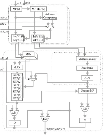
The computing circuit is independent of the MF implementation. In this paper a memory approach is used as an example. An architecture diagram is shown in Fig. 1.
Two big blocks construct the architecture diagram: a) A multi-plane fuzzifier for 2 input variables, a multi-plane each. b) An inference and defuzzifier block for a unique output variable. The MIN and Address Maker are multi-plane operations because they need information about all input variables.
Note that clock and reset signals are not shown in the architecture diagram. The applications need define: a) the memory block widths (like ADF, D and N), b) the register bank data and address widths (like RegVi, IdfVi and SOP).
Architecture details:
x Memory blocks:
q REG[vi] store the MF value of the input variables.
q IDF[vi] store the MF identifiers.
q SOP store the inference engine outputs,
q ADF is a pointer to the output fuzzy set,
q N holds the numerator value, and
q D holds the denominator value.
x Circuit blocks:
q Address Calculation: determines the pointer to REG and IDF register.
q MIN and MAX: compute the minimum and maximum values.
q Address Maker: determines the active rule for the inference engine.
q MF[vi] are the membership functions for each input variable value.
q MF-IDF[vi] are the membership function identifiers for each input variable value.
q Rule Bank holds the set of rules.
q Output-MF is the output MF for the input variable.
q ADD and DIVISION operations. Note that the division operation is not detailed.
x Control signals:
q SelVi is a pointer to REG/IDF registers.
q AB_PTR selects the address between SelVi (at inference time) and the computed address (at fuzzifier time).
-10-q IND addresses the SOP registers in the defuzzification stage.
q ADF_IND selects the address between IND (at defuzzification time) and ADF (at inference time). D. RESULTS
The FLC architecture has been used to develop a wide variety of applications. The selected implementation platforms were the Virtex or the xc4000 Xilinx FPGA families. The original design was generated in an automatic way by using a FLC generator [06] [11] [12] that produces VHDL in RTL (Register Transfer Level). The Xilinx Foundation v4 was used to generate the configuration bit-stream. In this paper 3 implementations are described.
In the Bart Kosko parking a truck in a load zone FLC [13] [14], the main features are: a) 2 input variables (with 7 and 5 MF). b) 1 output variable (with 7 MF). c) 35 rules (with 2 antecedents
and 1 consequent). d) 22 microinstructions at a maximum frequency. The FLC runs: a) in the Virtex at 18 MHz, so it produces a throughput of 818 K FIPS (Fuzzy Inferences Per Second) and 28 M FRPS (Fuzzy Rules Per Second). b) In the xc4000 at 12 MHz, 545 K FIPS and 19 M FRPS.
In the inverted pendulum FLC [15], the main features are: a) 2 input variables (both with 7 MF). b) 1 output variable (with 7 MF). c) 49 rules. d) 16 microinstructions. The pendulum runs: a) in the Virtex at 21 MHz, 131 K FIPS and 64 MFRPS. b) In the xc4000 at 11 MHz, 687 K FIPS and 33 M FRPS.
In the Aptronix autofocus [16] FLC, the main features are: a) 3 input variables (with 3 MF). b) 3 output variables (with 3 MF). c) 20 rules. d) 14 microinstructions. The autofocus runs: a) in the Virtex at 23 MHz, 1642 K FIPS and 32 M FRPS. b) In the xc4000 at 14 MHz, 1 M FIPS and 20 M FRPS.
MF(x)
var1
add MF-IDF(x)
Address Computing
0 1
RegV1(0) RegV1(1)
IdfV1(0) (1) idfV1
MIN
MAX
SOP(0) SOP(1) SOP(2) SOP(3) SOP(4) SOP(5) SOP(6) SOP(7)
1 0 ADF
add
D iv D
Output MF
N
OutputValueVar1 selV 1
A B_ptr
adf_ind
ind
var2
selV 2
Address maker
[image:3.595.134.484.255.709.2]Rule bank
Fig. 1.-Multi-resource architecture
-11-4. INTRODUCTION TO DIGITAL NEURAL NETWORKS Artificial neuronal networks (ANN) can be classified into two groups based on the degree of parallelism obtained in the diverse developments.
There are developments with high degree of parallelism that implement the architecture of the network with all their neuronal interconnections. Those developments are limited to small networks consisting generally of one hidden level with less than 10 neurons.
On the other hand, there are developments of low (or null) level of parallelism that completely implement the functionality of a single neuron plus a control unit. That unit successively feeds the neuron with sets of weights and input values to obtain a valid output result. This last alternative allows implementing time multiplexed hardware circuits with a high advantage in area to risk of a reduced performance.
Time Multiplexed neural networks are commercially available whereas other designs are taken ahead by many research and academic groups.
The two main categories consist of neurocomputers based on standard integrated circuits and ASIC. The first ones are accelerator boards that optimize the speed of calculation in conventional computers (PC like or workstation). In these cases, where standard components are used, the designers can be concentrated totally in the development of a particular technology. In the second, several alternatives and technologies of implementation can be chosen for the neuronal accomplishment of chips, like digital, analog or hybrid neurochips.
The direct implementation in circuits generally alters the exact operation of the original processing elements (analyzed or simulated). It is due to the limitation in precision. The influence of this limited precision is of great importance for the correct operation of the original paradigm. Because of this many designers have dedicated much time to study these topics. In order to obtain implementations on great scale, several neurochips must be interconnected to create systems of greater complexity, with advanced communication protocols.
5. NEURAL NETWORK ARCHITECTURE
The developed ANN has two essential features. By one side, a data route is highly used by segmented components (multiplier, adder, data/results memory), which allows a high performance of the data circuit, with the consequent speed increase. On the other side, the possibility of microprogramming the data route, allows a great flexibility to implement different ANN architectures: feedforward, cyclic, acyclic, and so on. The general circuit building blocks are depicted in Fig. 2 [17].
As it may be seen, the proposed ANN datapath is a circular pipeline of a multiplier, an accumulator, an activation function module and data memory; all of them pipelined as well.
[image:4.595.327.551.45.172.2]The multiplier has two 8-bit inputs, one 16-bit output, with a total of 360 registers and 64 basic 1-bit multipliers. Although this 8-bit configuration for internal data can be easily rearranged, a new configuration of more bits will increase the resources (cost) needed for the implementation of the multiplier with a quadratic factor. The 8-bit data route allows a new result in each clock cycle, being of 16 cycles the latency for each computation. The accumulator output is wired to the activation function circuit.
Fig. 2: Developed ANN building blocks. A. THE ACTIVATION FUNCTION
A common approach for this activation function in ANN is the sigmoid function of eq. (1).
(1) In the software implementations there is not a major drawbackon computing eq. (1). However, from the hardware standpoint, there is a high cost on implementing both a lookup table for the exponential function, and the division operation. Instead, a usual approximation in the hardware world is [18]:
¸ ¸ ¹ · ¨
¨ © §
1
1 2 1 ) (
x x x
y (2)
This approach, although simpler than the one of eq. (1), still needs the module and the division computation. In this work a third proposal is used. It consists of an approximation of eq. (1) with several polynomial functions in powers of 2, conforming a piecewise linear function [19] [20]. Particularly, the input for the developed circuit was a 16-bit integer [-32768..32767], and its output is a signed 8-bit integer [-128..127]. Table 1 shows the six input ranges with their corresponding output ranges.
INPUT OUTPUT 0..1023 0..31 1024..2047 32..63 2048..4095 64..95 4096..5119 96..111 5120..6143 112..115 6144..7167 116..119 7168..8191 120..123 8192..12287 124..127 12288..32767 127 Table 1: Polynomial functions in power of 2 for the
approximation of the exponential function.
In Fig. 3 a comparison among the three described approaches for the activation function is depicted (eq. (1), (2), and Table 1). It may be seen that the third implementation is closer to eq. (1) than the proposal of eq. (2). Then, this option was used for the present application. The selected approach, as well as the remaining presented components were described in VHDL. Then, it is immediate to replace for instance the module in the data route to change the activation function of the ANN. In a following section, it will be shown how easy it is to change the synaptic weights and the data/results memory from the parameters defined for a specific ANN.
[image:4.595.349.530.458.586.2]-12-Fig. 3: Three approaches for the sigmoid activation function [eq. (1) (continuous line), eq. (2) (discontinuous
line), table1 (doted line)] B. PRECISION ANALYSIS
[image:5.595.67.282.46.159.2]As in any digital circuit, in this case there is a trade off between precision and physical parameters like area and computing speed. Then, it seems interesting to analyze the behavior of the ANN when trained with different data series and different internal precision (number of bits). An exhaustive study of this was left for a near future. Nevertheless, the ANN was studied in simulation using representations for the weights and data of 20, 16, 12 and 8 bits. The results obtained for this last case were considered acceptable for the present application, as shown in Fig. 4.
Fig. 4: The simulated ANN output with double precision (in gray) vs. 8 bits precision (in black). C. PROGRAMMING THE ANN
The proposed architecture is programmed according to two main parameters to be selected previously. Once this step is fulfilled, a microprogram should be written to control the computations of the particular design.
D. PARAMETER DEFINITION
The first parameter to consider is the number of cells of the data/results row (L), according to:
L = max (N – 1) (3)
where N is the number of neurons in two contiguous level. This L
row must always be able to store the outputs of the just computed level (data) plus the results of computing each neuron in the present level. The second parameter is the size of the weight’s memory (Swm), which will store all of ANN weights.
Example 1: a classical feedforward ANN of nine neurons in the hidden layers and four inputs and three outputs is described according to Fig. 5.
E. MICROPROGRAM CREATION
From two levels of abstraction, a software tool (assembler) was developed to analyze the precedence relationships in the computations needed in the network under design. The highest level of abstraction generically describes which kind of neural
[image:5.595.343.528.73.188.2]network is under development. The present supported types are feedforward and Hopfield, synchronic and asynchronic [21].
Fig. 5: Parameters definition of an ANN Example II: the feedforward ANN of Fig. 5 is defined as:
Net <name> Description type feedforward Input : 4 Output : 3 Hidden : 4 , 5 End <name>
Example III: a given Hopfield ANN (Fig. 6) is defined as: Net <name> Description
type sync Hopfield Nodes : 3
End <name>
Fig. 6. Hopfield ANN.
The synchronous or asynchronous feature of the Hopfield ANN is achieved by the microprogram. In the first case the neurons are all updated in each clock cycle. In the second, the neurons are updated sequentially. This high level description only allowed the generation of simple and remarkably regular neural nets, but did not permit to outline more specific details about the neurons interaction of a particular design. Then, a lower level of description was needed, in which neuron dependencies were explicitly stated. This was achieved by programming as shown in Example IV.
Example IV: a more detailed description of a feedforward ANN with 4 inputs, 2 outputs and a hidden layer of 3 neurons, in a lower level of abstraction (Fig. 7)
Net <name> Description type Feedforward
Nodes: A, B, C, D, E, F, G, H, I Weights: w1..w18
Input Nodes: A, B, C, D Output Nodes : H, I Relation
E = A * w1 + B * w2 + C * w3 + D * w4 F = A * w5 + B * w6 + C * w7 + D * w8 G = A * w9 + B * w10 + C * w11 + D * w12 H = E * w13 + F * w14 + G * w15
I = E * w16 + F * w17 + G * w18 End Relation
End <name>
[image:5.595.72.270.340.434.2]-13-Fig. 7. Feedforward ANN.
From this description, the assembler can settle down the introduced parameters L (equation (3)) and Swm which will be 6
and 18 cells respectively for this example. The microprogram generation is based on these specifications, which map into a set of microinstructions that the control unit successively stores in the corresponding register. This register has 2*L bits, coding one
among the four possible operations for each cell of the data/results row. They are presented in Table 2.
Rotation (C) The cell receives the row output value No operation (N) The cell is not modified
Shift (S) The cell receives the value from its prior one (left)
[image:6.595.342.534.43.151.2]Datum load (L) The cell is loaded with the value from the activation function or the input data Table 2: Microinstructions of the microprogram.
The resulting microprogram of Example VI is partially shown in Table 3. The microprogram puts the resulting values of computing each neuron in the data row, in a position such that this value operates with the corresponding weight when going out of the row. To achieve this, weights are stored in a circular buffer of ROM memory. In this way, the ANN behaves like a systolic system, multiplying a value from the data/results row and a corresponding synaptic weight in each clock cycle. This product (a partial result) is stored until every input to each neuron is processed. Once the output of a processed neuron is obtained, it is crossed through the activation function and the result is stored in the data row, in the cell pointed by the current microinstruction. This procedure is illustrated in Fig. 8.
C Microinst Row state Operation Comments 0 NNNNNL _ _ _ _ _ A _ initial data
load 1 NNNNLN _ _ _ _ B A _
2 NNNLNN _ _ _ C B A _ 3 NNLNNN _ _ D C B A _
4 NNCSSS _ _ A D C B Acc = A * w1 A is recycled 5 NNCSSS _ _ B A D C Acc += B * w2 B is recycled 6 NNCSSS _ _ C B A D Acc += C * w3 C is recycled 7 NLCSSS _ E D C B A E = Acc += D
* w4
D is recycled and E is
loaded ... ... ...
11 SLSSSS _ F E D C B F = Acc += A * w4
shift and F is loaded 12 SSSSSS _ _ F E D C Computation of
G
[image:6.595.111.234.57.154.2]global shift ... ... ...
Table 3: Part of the microprogram of Example VI.
Fig. 8: Data flow in the ANN. F. RESULTS
Two alternatives of the presented architecture were implemented: STANDARD; the displayed design. OPTIMIZED; optimized version of the design. Redundant multiplexors in data memory are reduced or eliminated. This alternative reduces the size of the data memory and control unit.
With the Xilinx Foundation tool an important difference in synthesis and implementation speed was observed. In fact, the F3.1i version was around 40% superior in average to the F2.1i version.
With reference to the number of decisions per second (DPS) it was observed that, independently of the circuit frequency, DPS value is inversely proportional to the complexity of the neuronal network (in terms of inputs and hidden neurons).
The number of CLBs increases sensibly in circuits with more inputs or hidden neurons. This is due to the increase in the data memory cells but mainly by the increase in complexity in the control unit (as well by the higher number of control signals that must handle).
The operating frequency for all the versions tends to diminish when increasing the size of the circuit. This effect is not itself related to the datapath, since it is the same for all implementations. In fact, it is related to two factors: first, the increase of the circuit size which goes in detriment of more optimal locations and connections (place and routing) and forces to use tracks of smaller speed. Secondly, the synthesis of control units of higher number of signals increases the depth of logic in the design increasing the clock period of the circuit.
Fig. 9 shows several implementations of the architecture with F3.li version of Xilinx Foundation tool. All circuits have only one hidden level with two neurons and 16-bit precision datapath.
Inputs CLB Flops Frec. (MHz)
Logic
deep DPS 10 182 270 12,032 10 802133,3 12 207 280 12,839 12 755235,3 14 218 288 13,265 10 698157,9
16 230 296 11,369 11 541381
18 222 304 10,199 11 443434,8
20 257 313 8,773 10 350920
22 267 321 9,762 10 361555,6 24 272 329 9,490 11 327241,4
[image:6.595.53.293.259.346.2]26 284 337 10,784 11 347871
Fig. 9: Implementation results of the architecture with several inputs.
[image:6.595.52.294.515.714.2] [image:6.595.333.546.573.726.2]-14-6. CONCLUSIONS
This paper shows an efficient digital approach to develop an ANN or an FLC. The development approach to obtain a specific circuit (ASIC, FPGA) is automatically performed according to the following steps: a) Controller definition in a description language. b) Circuit and control program generation. c) Automatic synthesis of the design by using the commercial FPGA development tools. d) FPGA and memory configuration. The FPGA shows to be an efficient development platform, but they need to be in an efficient card that provides: a) Access to external RAM. b) Connection to multiple clocks running at different rates. c) Connectivity to a great number of external lines. d) Low power consumption. e) A prototyping area. As a prototyping platform, the card must have a great number of interconnection lines connected straight to the computer I/O ports.
The developed tool has been implemented in Delphi. It parses the input language while loading, and then, the interface lets the user to select which kind of synthesis is needed. This prototype includes generators for: a) VHDL in RTL (automatic synthesis allowed). b) Prototyping languages like VHDL in behavioral descriptions, C and Pascal.
As a future work, the synthesis tools will be adapted in order to support: a) Other tools, such as Viewlogic, standard cells library. b) Analogical platforms. c) Multi-resource architectures (multi-ALU pipelined data path) in the FLC. d) Area and speed metric estimation before the place and route process.
REFERENCES
[01]. “Expert System on a Chip: An Engine for Real-Time Approximate Reasoning”. Togai M. and Watanabe H. IEEE Expert, vol. 1, Nro. 3, pp: 55-62.
[02]. “A VLSI Fuzzy Logic Controller with Reconfigurable, Cascadable Architecture”. Watanabe H, Dettlof W. and Yount K. IEEE Journal on Solid-State Circuits, vol. 25, nro. 2.
[03]. “Architecture of a PDM VLSI Fuzzy Logic Controller with Pipelining and Optimized Chip Area”. Ungering A., Thuener K. and Gosser K. Proc. of IEEE International Conference on Fuzzy Systems, pp: 447-452.
[04]. “7.5 MFLIPS Fuzzy Microprocessor using SIMD and Logic-in-Memory Structure”. Sasaki M. Ueno F. and Inoue T. Proc. of IEEE International Conference on Fuzzy Systems, pp: 527-534.
[05]. “Customized Fuzzy Logic Controller Generator”, Acosta N., Deschamps J-P. and Sutter G. Proc. of IFAC-MIM´97, Vienna, Austria, February 1997, pp: 93-98.
[06]. “Automatic Program Generator for Customized Fuzzy Logic Controllers”, Acosta N., Deschamps J-P. and Sutter G. Proceedings of IFAC-AART´97, Vilamoura, Portugal, April 1997, pp: 259-265.
[07]. “Hardware design of Asynchronous Fuzzy Controllers”. Costa A., De Gloria A. and Olivieri M. IEEE Trans. on Fuzzy Systems, vol. 4, Nro. 3, August. 1996, pp.: 328-338. [08]. “Dedicated Digital Fuzzy Hardware”. Hung D. L. IEEE
Micro, vol. 15, nro. 4, pp: 31-39.
[09]. “Algoritmo de optimización de funciones reticulares aplicado al diseño de Controladores Difusos”. Deschamps J-P and Acosta N. XXV JAIIO, pp: 1.17-1.27. September 1996.
[10]. “On Fuzzy Associative Memory with Multiple-rule Storage Capacity”. Chung F. and Lee T. IEEE Trans. on Fuzzy Systems, vol. 4, Nro. 3, August, pp: 375-384.
[11]. “Optimized active rule fuzzy logic custom controller”, Int. Symp. on Engineering of Intelligent Systems (EIS'98),
organizado por IFAC (International Federation of Automatic Control), Tennerife, España. February 1998. Acosta N., Deschamps JP. y Garrido J. Pp. 74-79.
[12]. “Materialización de Controladores Difusos Activos”, Acosta N. CACIC'2001. October 2001. El Calafate (Arg). [13]. “Adaptative Fuzzy Systems for Backing up a
Truck-and-trailer”, Kong S. and Kosko B. IEEE Trans. Neural Networks, Vol. 3, Nro. 2, pp.: 211-223, March 1992. [14]. “Neural Network and Fuzzy Systems”, Kosko B. Prentice
Hall, chapter 9.
[15]. “Robust fuzzy control of nonlinear systems with parametric uncertainties”, H Lee, B Park & G Chen. IEEE Trans. on Fuzzy Systems, Vol. 9, Nro. 2, April 2001. Pp: 369-378. [16]. “FuzzyNET”, Aptronix. http://www.aptronix.com.
[17]. “Hardware Implementation of a segmented data route for Neural Networks”, Tosini, M. VI Workshop Iberchip, IWS´2000, Sao Paulo, Brazil, pp. 292-299, March 2000. [18]. “Using and Designing Massively Parallel Computers for
Artificial Neural Networks”, Nordström, T. and Svensson, B. Journal of Parallel and Distributed Processing, vol. 14, no. 3, pp. 260-285, 1992.
[19]. “Efficient implementation of piecewise linear activation function for digital VLSI neural networks”, Myers, D. J. and Hutchinson, R. A. Electronic Letters, Vol. 25, pp. 1662-1663, 1989.
[20]. “Simple approximation of sigmoidal functions: realistic design of digital neural networks capable of learning”, Alippi, C. and Storti-Gajani, G. Proc. IEEE Int. Symp. Circuits and Systems, pp. 1505-1508, 1991.
[21]. “Computers and Symbols Versus Nets and Neurons”, Gurney, K. UCL Press Limited, UK, 1995.