THERMOMECHANICAL PERFORMANCE OF FR-4 LAMINATES IN
THE MANUFACTURING PROCESS OF PRINTED CIRCUIT
BOARDS
POR
CARLOS ALFONSO RODRÍGUEZ VÁZQUEZ
COMO REQUISITO PARA OBTENER EL GRADO DE
DOCTOR EN INGENIERÍA DE MATERIALES
UNIVERSIDAD AUTÓNOMA DE NUEVO LEÓN
FACULTAD DE INGENIERÍA MECÁNICA Y ELÉCTRICA
SUBDIRECCIÓN DE ESTUDIOS DE POSGRADO
THERMOMECHANICAL PERFORMANCE OF FR-4 LAMINATES IN THE
MANUFACTURING PROCESS OF PRINTED CIRCUIT BOARDS
POR
CARLOS ALFONSO RODRÍGUEZ VÁZQUEZ
COMO REQUISITO PARA OBTENER EL GRADO DE
DOCTOR EN INGENIERÍA DE MATERIALES
Acknowledgment
This work is dedicated primarily to God and my family who has been at all times to support me to meet each of the goals that, my father Alfonso Rodriguez and my mother Patricia V´azquez they push me to reach my personnel targets being aware of everything that needed.
I appreciate the support of Dr. Mois´es Hinojosa for being an excellent advisor, their support was very important for the research work, his collaboration is reflected in the objectives and expectations reached, I appreciate his support for conferences and congress participation.
I appreciate to Dr. Javier Morales, Dr. Jorge Aldaco and Dr. Roberto Cabriales really for helping during the project meetings we had, making an excellent analysis for knowledge contribution.
I thank Dr. Carlos Morillo and his team at the University of Maryland for enable me and help me to realize experimentation during my stay at CALCE, I learned everything necessary for PCB’s characterization and the state of the art.
The National Council of Science and Technology (CONACYT) for providing economic support during these 3 years.
Thanks to Yazaki, especially for Ing. Luis Montes de Oca, EI (Electronic Instru-ments) manager and Ing. V´ıctor Salinas Fox who was an important member during the project, Ing. Karla Pe˜na my supervisor at Yazaki for their collaboration to carry out this research, also the staff involved in PCB assembly process at YIM (Yazaki Instruments Monterrey).
Acknowledgment i
Abstract x
1 Introduction 1
1.1 What is a Printed Circuit Board? . . . 1
1.1.1 Base Materials for Printed Circuit Board . . . 2
1.2 Assembly Process of Printed Circuit Board . . . 3
2 Literature Overview 4 2.1 PCB’s Base Materials . . . 4
2.1.1 Resins Systems . . . 5
2.1.2 Reinforcements . . . 6
2.1.3 Conductive Material . . . 8
2.2 PCB Fabrication . . . 10
2.3 Reflow Process . . . 11
2.4 Thermal Properties of PCB Materials . . . 15
2.4.1 Glass Transition Temperature . . . 15
2.4.2 Decomposition Temperature . . . 16
2.4.3 Coefficient of Thermal Expansion . . . 17
2.4.4 Time to delamination . . . 19
2.4.5 Water Absorption . . . 21
2.5 “Bow” and “Twist” . . . 21
3 State of the Art 26 3.1 Material Properties . . . 26
3.2 Reflow Oven Process . . . 27
3.3 Warpage . . . 28
3.4 Summary . . . 28
iv Contents
4 Motivation, General Objective, Specific Objectives and Hypothesis 30
4.1 Motivation . . . 30
4.2 General Objective . . . 31
4.3 Specific Objectives . . . 31
4.4 Hypothesis . . . 32
5 Experimental Methodology 33 5.1 Material Characterization . . . 34
5.1.1 PCB configuration . . . 34
5.1.2 Thermal Properties . . . 34
5.2 Reflow Oven . . . 40
5.2.1 Temperature Profiles . . . 40
6 Results and Discussion 42 6.1 Glass Transition Temperature (Tg) . . . 42
6.2 Decomposition Temperature (Td) . . . 46
6.3 Coefficient of Thermal Expansion . . . 48
6.3.1 Coefficient of Thermal Expansion in the “x” axis . . . 48
6.3.2 Coefficient of Thermal Expansion in the “y” axis . . . 50
6.3.3 Coefficient of Thermal Expansion in the “z” axis . . . 53
6.4 Time to Delamination . . . 56
6.5 Water Absorption . . . 58
6.6 Bow and Twist Measurement . . . 58
6.6.1 PCB “bow” after first reflow . . . 58
6.6.2 PCB “bow” after second reflow . . . 59
6.6.3 PCB “twist” after first reflow . . . 60
6.6.4 PCB “twist” after second reflow . . . 61
6.7 Temperature Profile . . . 63
6.8 Summary of Results . . . 64
7 Conclusions and Contributions 68 7.1 Conclusions . . . 68
7.2 Contributions . . . 70
A Heat Transfer for Base Materials 71
C Bow Results 73 C.1 Bow results after first reflow . . . 73 C.2 Bow results after second reflow . . . 73
D Twist Results 75
D.1 Twist results after first reflow . . . 75 D.2 Twist results after second reflow . . . 75
List of Figures
1.1 Sierra GMC indicators panel . . . 1
1.2 Printed Circuit Board . . . 1
1.3 PCB configuration . . . 2
1.4 PCB’s manufacturing process diagram . . . 3
2.1 Difunctional epoxy resin reaction . . . 5
2.2 Brominated difunctional epoxy resin reaction . . . 5
2.3 Tetrafunctional epoxy resin . . . 6
2.4 Multifunctional fenol novolac epoxy resin . . . 6
2.5 Glass fiber styles . . . 7
2.6 “Treating” fiberglass cloth with resin . . . 10
2.7 Laminate pressing . . . 11
2.8 Reflow oven . . . 11
2.9 Reflow oven stages . . . 12
2.10 Sn-Ag-Cu Solder paste phase diagram [11] . . . 13
2.11 Sn-Pb Solder paste phase diagram . . . 13
2.12 Cooling area . . . 14
2.13 PCB’s Electronic components failure due to PCB “warpage” . . . 14
2.14 Capacitor failure due to PCB “warpage” . . . 15
2.15 Schematic representation to obtain Tg [19] . . . 16
2.16 Decomposition temperature chart for different FR-4 types . . . 17
2.17 Representation to obtain coefficient of thermal expansion . . . 18
2.18 CTE axes . . . 19
2.19 Representation to obtain time to delamination . . . 20
2.20 “Bow” . . . 22
2.21 “Twist” . . . 22
2.22 “bow” y “twist” areas identification . . . 23
2.23 PCB schematic representation of thickness, diagonals and lengths . . 24
2.24 PCB schematic representation to obtain % of bow . . . 24
2.25 Schematic representation to obtain % of twist . . . 25
5.1 Experimental procedure . . . 33
5.2 PCB cross sectional view showing PCB ayers configuration . . . 34
5.3 Specimens at different areas of PCB . . . 35
5.4 Preheating oven . . . 36
5.5 DSC Netzch pegasus . . . 37
5.6 Specimens to obtain glass transition temperature . . . 37
5.7 Dynamic Mechanical Analysis (DMA) . . . 38
5.8 Specimens to obtain decomposition temperature . . . 38
5.9 TMA (Thermo Mechanical Analyzer) . . . 39
5.10 Specimens to obtain coefficient of thermal expansion . . . 39
5.11 Specimens water absorption performed . . . 40
5.12 Device to obtain height of the PCB’s . . . 40
5.13 PCB to measure oven temperatures . . . 41
5.14 Standard PCB reflow process profile . . . 41
6.1 Glass transition temperature chart top area . . . 43
6.2 Glass transition temperature chart middle area . . . 43
6.3 Glass transition temperature chart bottom area . . . 44
6.4 Decomposition temperature chart . . . 46
6.5 Specimen 1 decomposition temperature chart . . . 47
6.6 Specimen 2 decomposition temperature chart . . . 47
6.7 Coefficient of thermal expansion “x” axis at top area . . . 48
6.8 Coefficient of thermal expansion “x” axis at middle area . . . 49
6.9 Coefficient of thermal expansion “x” axis at bottom area . . . 49
6.10 Coefficient of thermal expansion “y” axis at top area . . . 51
6.11 Coefficient of thermal expansion “y” axis at middle area . . . 51
6.12 Coefficient of thermal expansion “y” axis at bottom area . . . 52
6.13 Coefficient of thermal expansion “z” axis at top area . . . 53
6.14 Coefficient of thermal expansion “z” axis at middle area . . . 53
6.15 Coefficient of thermal expansion “z” axis at bottom area . . . 54
6.16 Time to delamination results at the top . . . 56
6.17 Time to delamination results at the middle . . . 57
6.18 Time to delamination results at the bottom . . . 57
viii List of Figures
6.20 PCB “bow” results after second reflow . . . 60
6.21 PCB “twist” results after first reflow . . . 61
6.22 PCB “twist” results after second reflow . . . 62
6.23 TC 1 temperature vs time . . . 63
6.24 TC 2 temperature vs time . . . 63
6.25 TC 3 temperature vs time . . . 63
6.26 TC 4 temperature vs time . . . 63
1.1 PCB base materials . . . 2
2.1 PCB’s classification [3]. . . 4
2.2 Glass fiber chemical composition . . . 7
2.3 Traditional woven glass fabric styles [8] . . . 8
2.4 Types of conductor material [3]. . . 8
5.1 Thermal properties standards . . . 35
5.2 Material thermal properties . . . 36
6.1 Glass transition temperature results for the 3 areas . . . 44
6.2 Thermal conductivity of base materials [3] . . . 45
6.3 Specimens mass to obtain decomposition temperature . . . 46
6.4 Results at 3 areas for “x” axis . . . 50
6.5 Results at 3 areas for “y” axis . . . 52
6.6 Results at 3 areas for “z” axis . . . 54
6.7 CTE results at 3 areas . . . 55
6.8 Water absorption results . . . 58
A.1 Heat transfer of base materials . . . 71
B.1 PCB’s dimensions . . . 72
C.1 PCB bow results after first reflow . . . 73
C.2 PCB bow results after second reflow . . . 74
D.1 PCB twist results after first reflow . . . 75
D.2 PCB twist results after second reflow . . . 76
Abstract
Printed Circuit Boards (PCB’s) are an important component for any electronic de-vice, they can be found in cell phones, computers, tablets, televisions, radios, remote controls, among others. In automotive industry, PCB’s are incorporated into the board containing tachometers, water, oil, gasoline levels and all signals displayed on the board. PCB’s contain electronic components such as: electric motors, resistors, capacitors, micro-controllers and LED’s, just to name a few. To join them, a solder paste of tin, silver and copper alloy (Sn-Ag-Cu) is applied on the PCB surface; then the PCB is processed into a reflow oven at temperature range of 24oC-250oC allow-ing the solder paste to flow and join the electronic components with the PCB, an operation called “reflow process”.
In 2006 the Restriction of Hazardous Substances (RoHS) prohibited the use of lead (Pb) in solder paste, which has a melting temperature around 180oC, whereas lead-free solder pastes have a melting point around 230oC, 30oC-40oC higher than Pb solder paste, this has generated PCB thermo mechanical problems due to the temperature increase at which the material is exposed. Typical problems are related with deformations of the PCB in the reflow process, such as “warpage”, which is a deformation along the “z” axis and is accompanied by other phenomena called “bow” and “twist’, “bow” is characterized by a curvature of cylindrical shape on both sides of the PCB whereas “twist” is characterized by the elevation of the cor-ners. “Warpage”, “bow” and “twist” affect subsequent processes such as: assembling engines, micro-controllers, improper electrical tests, false contacts, bending of elec-tronic components and fractures at the interphase between elecelec-tronic component and the PCB.
The present research work studies the relation between material thermal proper-ties, PCB configurations and reflow conditions with “warpage” “bow” and “twist” during the reflow process by the thermal characterization of base materials, deforma-tions measurements and temperature reflow profiles. Thermal properties obtained were: glass transition temperature (Tg), decomposition temperature (Td),
ficient of thermal expansion (CTE), time to delamination and %water absorption, deformations measurements were obtained on 30 PCB’s after exposure. Temperature profiles were obtained by placing thermocouples on the PCB.
Our results suggest that there is a discrepancy between the thermal properties obtained experimentally and data sheet provided by the supplier. PCB “bow” and “twist” data obtained exceeds the values established by the IPC-2221B standard and the temperature profiles met the requirements of the quality control in the company. It is found that there is a mismatch between temperature profiles, it is speculated a relationship with preferential deformations during reflow process.
Chapter 1
Introduction
1.1
What is a Printed Circuit Board?
Printed Circuit Boards (PCB’s) are an important component for any electronic de-vice. They can be found in cell phones, computers, tablets, televisions, radios, remote controls, among others [1]. PCB’s are used in the automotive industry, they are inte-grated into the automobiles panel indicators which contains speed, RPM tachometers and temperature, air bags, handbrake and safety signals on the board. Figure 1.1 shows the panel indicators of Sierra truck and figure 1.2 shows a PCB which it is behind the panel of figure 1.1.
Figure 1.1: Sierra GMC indicators panel
Figure 1.2: Printed Circuit Board
The first PCB’s were developed in the 1900’s, Albert Hanson described flat foil
conductors laminated to an insulating board in multiple layers, also Thomas Edison experimented with chemical methods of plating conductors in 1904. Arthur Berry in 1923 patented a print and etch method, while Max Schopp in USA obtained a patent. In the 1930’s Paul Eisler used a PCB for a radio and the PCB growing was during the World War II due to USA began to use technology on high volume applications [2].
PCB’s are made of different materials: resins, reinforcements, conductive ma-terial, flame retardants, curing agents and coupling agents [3]. The next section provides a general overview of how a PCB is made.
1.1.1
Base Materials for Printed Circuit Board
Figure 1.3 [4] is schematic representation of cross sectional view and shows how the PCB is made, there are resin/fiberglass layers, copper and fillers. Each mate-rial provides some specific property. Table 1.1 lists PCB base matemate-rials and their function.
Figure 1.3: PCB configuration
Table 1.1: PCB base materials
Material Function
Reinforcement (glass fiber) Provide electrical and mechanical properties Resins Acting to transfer thermal and mechanical loads Coupled agents Glass fiber and resins interfaces improvement Flame retardants Reduced flammability
Conductor material (copper) PCB interconnections
Cured agents Polymerization improvement
Accelerators Reduced cured time
Fillers Mechanical properties improvement
1.2. Assembly Process of Printed Circuit Board 3
motors, displays, micro-controllers among others. The next section explain briefly the electronic components assembly.
1.2
Assembly Process of Printed Circuit Board
A flow chart of electronic components assembly is presented in figure 1.4, “Reflow process” consists to processed the PCB into a oven to joint the electronics compo-nents with the PCB by a solder paste.
Figure 1.4: PCB’s manufacturing process diagram
Literature Overview
2.1
PCB’s Base Materials
There are many types of PCB’s, resin and fiberglass must be considered depending of the conditions to which the materials will be exposed. Table 2.1 shows a PCB classification according with the type of resin and reinforcement.
Table 2.1: PCB’s classification [3].
PCB Resin Reinforcement Flame retardant
FR-2 Fen´olic Cotton Yes
FR-3 Epoxy Cotton Yes
FR-4 Epoxy Glass fiber Yes
FR-5 Epoxy Glas fiber Yes
FR-6 Polyester Glas fiber wave Yes
G-10 Epoxy Glass fiber No
CEM-1 Epoxy Cotton/Glass fiber Yes CEM-2 Epoxy Cotton/Glass fiber No
CEM-3 Epoxy Glass fiber Yes
CEM-4 Epoxy Glass fiber No
CRM-5 Polyester Glass fiber Yes CRM-6 Polyester Glass fiber No CRM-7 Polyester Glass fiber Yes CRM-8 Polyester Glass fiber No
Flame retardant (FR-4) is the PCB most widely used in electronic industry with applications in toys, controls, calculators and computers. In the automotive industry, FR-4 is used in automobiles panel indicator, clocks, LCD’s, alarms, among others electronics devices incorporated into the vehicle. According with table 2.1 FR-4 is composed of epoxy resin and glass fiber as a reinforcement. Next sections provides
2.1. PCB’s Base Materials 5
in more detail these materials.
2.1.1
Resins Systems
Epoxy resins are the most efficient systems used for PCB’s due to the combination of good physical, mechanical and electrical properties with it’s low cost fabrication compared to high-performance resins systems. Epoxy resins systems are classified as: difunctional, tetra-functional and multifunctional. The prefix “di”, “tetra” and “multi” refers to the number of epoxy groups at the end of the molecular chain [7].
Difunctional Epoxy Resin
Bisphenol-A and epyclorodrine reaction is the most common epoxy resin systems for PCB’s. Bisphenol-A brominated provides flame retardancy. The reaction is schematically shown in figure 2.1.
Figure 2.1: Difunctional epoxy resin reaction
When the increase of flame retardancy becomes important, tetrabromobisphenol-A is added in the reaction as figure 2.2 shows, this is another system of difunctional epoxy resin called brominated epoxy resin doped.
Epoxy resin molecular weight depends of the group repetitions at the center of the molecule and final properties depends on: molecular weight, curing agents, glass transition temperature (Tg) and decomposition temperature (Td).
Tetra and Multifunctional Epoxy Resins
Two or more epoxy functional groups per molecule increases higher glass transi-tion temperatures and improve physical and thermal properties. These epoxy resins systems are classified based on glass transition temperature ranges, 125oC-145oC, 150oC-165oC and above 170oC. There are epoxy resins systems with glass transi-tion temperatures above 190oC, which has better properties, but they are expensive. Figures 2.3 and 2.4 are examples of these type of epoxy resins systems.
Figure 2.3: Tetrafunctional epoxy resin
Figure 2.4: Multifunctional fenol novolac epoxy resin
2.1.2
Reinforcements
2.1. PCB’s Base Materials 7
Table 2.2: Glass fiber chemical composition
Elements Style E Style NE Style S
Silicon dioxide 52-56 52-56 64-66
Calcium oxide 16-25 0-10 0-0.3
Aluminum oxide 12-16 10-15 24-26
Boron oxide 5-10 15-20
-Sodium oxide and Potassium oxide 0-2 0-1 0-0.3
Magnesium oxide 0-5 0-5 9-11
Iron oxide 0.05-0.4 0-0.3 0-0.3
Titanium oxide 0-0.8 0.5-5
-Fluorides 0-0.1 -
-complement the properties of epoxy resin systems which were being rapidly deployed in electronics [8]. However, the most widely used as base material is “E” glass fiber, offering good mechanical and chemical electrical properties for a reasonable cost.
Glass fiber is fabricated in different “styles” as figures 2.5a, 2.5b and 2.5c shows, which are 1080, 2116 and 7628 styles respectively and they are the most commonly used for PCB’s. Depending of the PCB thickness the number of layers of the style must be selected.
(a) 1080 (b) 2116 (c) 7628
Table 2.3 shows the traditional arrangements available [8].
Table 2.3: Traditional woven glass fabric styles [8]
Style Glass thickness (mm) Weight (gsm) Threads per cm
7628 0.17 203 17.3 x 12.2
2116 0.095 104 23.6 x 22.8
2125 0.09 87 15.7 x 15.4
2113 0.079 78 23.6 x 22.0
1080 0.05 47 23.6 x 18.5
106 0.033 24 22.0 x 22.0
In the future PCB base materials will no doubt utilize even better fibers and resins and will incorporate entirely new materials, including those on the nano scale. We are indebted to the researches and developers worldwide who continue to advance our knowledge and produce ever more advanced and functional materials to transform the designers dreams into reality [8].
2.1.3
Conductive Material
The main conductive material used in PCB’s is copper. Table 2.4 shows the different grades of copper.
Table 2.4: Types of conductor material [3].
Grade Foil Description
1 Standard electrodeposited (STD-Type E) 2 High-ductility electrodeposited (HD-Type E) 3 High-temperature elongation electrodeposited
(HTE -Type E)
4 Annealed electrodeposited (ANN-Type E) 5 As rolled-wrought (AR-Type W)
6 Light cold rolled-wrought (LCR-Type W) 7 Annealed-wrough (ANN-Type W)
8 As rolled-wrough low-temperature annealable (LTA-Type W) 9 Nickel, standard electrodeposited
10 Electrodeposited low temperature annelable (LTA-Type E)
2.1. PCB’s Base Materials 9
The most used is electro deposited grade 1 and grade 3. They are produced by electrochemical process where copper is first dissolved in a sulfuric acid solution. Copper sulfate/acid solution is then used to electroplate copper. Grade 3 commonly refers to the elongation at high temperatures, so it is a constituent for multilayer printed circuit boards. The increase in ductility at elevated temperatures provides resistance circuit when thermal stresses are generated and expands in the “z” axis. As a fabrication process improvement there are surface treatments to obtain good adhesion, some of them are described [3].
1. Bonding treatment: coatings of zinc, nickel or brass are introduced. Helps to prevent heat and chemical degradation copper links with the resin during manufacturing process. These coatings typically increase the thickness and color variation.
2. Thermal barriers: A coating of zinc, nickel, or brass is usually applied over the nodules. This coating can prevent thermal or chemical degradation of the foil to resin bond during manufacture of the laminate, the printed circuit, and the circuit assembly. These coatings typically measure several hundred angstroms in thickness and vary in color due to the specific metal-alloy used, although most treatments are brown, gray, or a yellow mustard color.
3. Antioxidants coatings: In contrast to the other coatings, these treatments are virtually always applied to both sides of the foil. Although many of these treat-ments are chromium based, organic coatings can also be utilized. The primary purpose of these treatments is to prevent oxidation of the copper foil during storage and lamination. These coatings are usually less than 100 angstroms thick and are typically removed by the cleaning, etching, or scrubbing processes normally used at the start of printed circuit manufacturing processes.
4. Coupled agents: The use of coupling agents, primarily silanes such as those used to promote fiberglass to resin adhesion, can also be used on copper foils. These coupling agents can improve the chemical bond between the foil and the resin system and can also be used to help prevent oxidation or contamination.
2.2
PCB Fabrication
The first step is coating a resin system onto the woven fiberglass cloth. Rolls of fiberglass cloth are run through equipment called treaters. The fiberglass cloth is drawn through a pan containing the resin system and then precise metering rolls help control thickness, as figure 2.6 shows.
Figure 2.6: “Treating” fiberglass cloth with resin
Next the cloth is pulled through a series of heating zones, which utilize forced air convection, infrared heating, or a combination of the two. In the first set of zones, solvent used to carry the resin system components is evaporated off. Subsequent zones are dedicated to partially curing the resin system. Finally, the prepeg is rewound into rolls or cut into sheets.
Control of the resin/glass ratio, the degree of cure of the resin and cleanliness are critical. Prepegs are stored in temperature and humidity controlled environments. Temperature affect the degree of cure of the resin and therefore its performance in laminate or multilayer circuit pressing. Moisture can affect the performance of many curing agents and accelerators, the performance of the resin system during lamination, humidity it also important to control during prepeg storage. Absorbed moisture that becomes trapped during lamination cycles can also lead to blisters or delaminations within the laminate or multilayer circuit.
2.3. Reflow Process 11
Figure 2.7: Laminate pressing
After laminates are finished next step is to print electronic designs on their sur-face, also drilling and protection surface are applied ready to incorporate the elec-tronics components by a reflow process, which is described in the next section.
2.3
Reflow Process
PCB’s are processed in a reflow oven in figure 2.8 to joint electronic components with PCB by tin-silver-copper (Sn-Ag-Cu) solder paste application, it has 2.95 m of length and the temperature range is from room temperature to 280oC, the average time of reflow process is five minutes.
Figure 2.8: Reflow oven
During reflow process the PCB travels through nine stages, 1 to 5 are preheating stages, 6 and 7 are heating stages and 8 and 9 are cooling stages, as shown in figure 2.9.
Figure 2.9: Reflow oven stages
lead free solder paste.
Lead-free solder paste
In 2006 RoHS prohibited the use of lead (Pb) [10] on solder pastes the use of lead-free solder pastes began. Pb-based solders were used for jewelry and making bonds between metals including the ancient pipes and aqueducts. Nowadays Sn-based solder alloys have replaced Pb-bearing solders in most applications, but replacing the Pb with Sn was no sufficient for solder joints, so alloying elements such as Cu and Ag to make Sn-Ag-Cu (SAC) alloys have brought performance necessary to meet requirements. Figure 2.10 (a) shows the phase diagram of the lead free solder, there are several invariant reactions. Fortunately, the ternary eutectic of primary interest, consisting of β −Sn, Ag3Sn, and Cu6Sn5 phases, exists at the Sn-rich
2.3. Reflow Process 13
Figure 2.10 (b) shows this corner in the established diagram, which displays the liquidus surface projected in a Cartesian plot where x-and y-axis represent the Cu and Ag concentration, respectively, with scales that are not the same. The liquidus surfaces merge at one point where the eutectic reaction occurs at 220oC approximately.
Figure 2.10: Sn-Ag-Cu Solder paste phase diagram [11]
On the other hand the conventional solder paste used before is composed basically of tin and lead (Sn-Pb) which has a melting temperature of 180◦C as figure 2.11
shows.
Figure 2.11: Sn-Pb Solder paste phase diagram
The drawback is that lead-free solder paste requires 35◦C- 40◦C above the melting
After reflow process there are cooling area as shown in figure 2.12. The cooling area has three stages, depending on the type of PCB and the side which it’s processing is the exposure time for cooling, typically cooling time is 40 seconds. First and second stages are at 24oC and third stage at 13oC; fans are installed trough the cooling area to accelerate air flow on the PCB cooling.
Figure 2.12: Cooling area
PCB’s has components on both sides, so the PCB is processed twice in the reflow oven. Once 2 sides are processed, electrical and functionality tests are performed, also motors and micro-controller are included on the PCB, finally the PCB is stored. During reflow process there are different failures due to PCB deformations, it has been reported failures due to PCB “warpage” [12], [13]. Pecht and co-authors studied the fracture resistance of welding and ceramic capacitors [14], figure 2.13 is a schematic representation of joint fracture between PCB and capacitor due to “warpage”.
Figure 2.13: PCB’s Electronic components failure due to PCB “warpage”
2.4. Thermal Properties of PCB Materials 15
Figure 2.14: Capacitor failure due to PCB “warpage”
Material thermal properties mismatch play an important role during reflow pro-cess, thermal conductivity of common FR-4 epoxy resin systems is 0.2-0.34 W/(moK), whereas the thermal conductivity of the fiber glass is lower than that of PCB FR-4 epoxy systems (0.02-0.04 W/(moK). This mismatch can limit the heat transfer [16], [17], there are other thermal properties that must be considered, such as: glass tran-sition temperature, decompotran-sition temperature, time to delamination, coefficient of thermal expansion, water absorption among others. Engineers must consider ma-terial thermal properties when a PCB is designed, the knowledge about mama-terial properties becomes an important factor for PCB reliability during the process. Next section provides an overview of material thermal properties.
2.4
Thermal Properties of PCB Materials
2.4.1
Glass Transition Temperature
expansion and the degree of cure of the resin system [3].
Figure 2.15 is a schematic presentation to determine glass transition temperature, which consists in draw two parallel lines, one under the transition zone and the other above the transition, identifying the midpoint and intersecting with “x” axis, the glass transition temperature is obtained [19].
Figure 2.15: Schematic representation to obtain Tg [19]
Several properties change as the Tg is exceeded, including the rate at which a material expands vs. temperature. Young’s modulus also decreases significantly as Tg is exceeded [20].
2.4.2
Decomposition Temperature
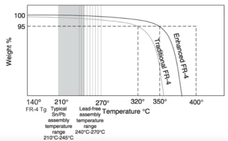
The material is heated at certain temperature, the resin system will begin to de-compose. The chemical bonds will begin to break down and volatile components will be driven off, reducing the mass of the sample. The decomposition tempera-ture (Td), describes the point at which this process occurs. Traditional Td is where 5 percent of the original mass is lost to decomposition. 5 percent is a very large number when multilayer PCB reliability is considered, however the reliability of tra-ditional FR-4 becomes important when exhibits 1.5-3 percent of weight loss. This level of decomposition can compromise long-term reliability or result in defects such as delamination during assembly, particularly if multiple assembly cycles or rework cycles are performed, when a material is tested for decomposition temperature 2% and 5% is recorded. Temperatures with lower levels of decomposition are important particularly for lead-free assembly [3].
2.4. Thermal Properties of PCB Materials 17
Figure 2.16: Decomposition temperature chart for different FR-4 types
The traditional FR-4 with 140oC of Tg material has a decomposition temper-ature of 320◦C by the 5 percent weight loss definition. The enhanced FR-4 has a
decomposition temperature of 350oC by the 5 percent weight loss definition. Many standard high-Tg FR-4 materials actually have decomposition temperatures in the range of 290-310oC, while the 140oC Tg FR-4 materials generally have slightly higher Td values. In figure 2.16 the shaded regions indicate the peak temperature ranges for standard tin-lead assembly and lead-free assembly [3].
Resin decomposition can result in adhesion loss and delamination. A 5% level of decomposition is severe, and intermediate levels are important for assessing re-liability since peak temperatures in lead-free assembly can reach onset points of decomposition [20].
2.4.3
Coefficient of Thermal Expansion
Coefficient of thermal expansion (CTE) of printed circuit boards have a great deal of influence on the reliability of solder joints in microelectronic packages [21]. CTE values above Tg are much higher than below Tg. Reflow process temperatures result in more total expansion for a given material. However, several mature lead-free compatible materials incorporate inorganic fillers that reduce CTE values [20].
Figure 2.17: Representation to obtain coefficient of thermal expansion
CTE below glass transition temperature is obtained selecting two points before the transition, in this case are “A” and “B”, they represents two temperatures (TA
and TB) and their thicknesses (LA and LB), values are substituted in the formula
2.1:
CT E(A−B) =
(LB−LA)106
L0(TB−TA)
(2.1)
Where:
• TA= temperature at “A” point in figure. 2.17.
• TB= temperature at “B” point in figure. 2.17.
• L0= thickness or initial length.
• LA= thickness or specimen length at point “A” in figure 2.17.
• LB= thickness or specimen length at point “B” in figure 2.17.
CTE above transition temperature is obtained selecting two points after the transition, which are “C” and “D”, temperatures (TC and TD) and their thicknesses
(LC and LD) are substituted in the formula 2.2:
CT E(C−D) =
(LD−LC)106
L0(TD−TC)
(2.2)
Where:
2.4. Thermal Properties of PCB Materials 19
• TD= temperature at “D” in figure 2.17.
• L0= thickness or initial length.
• LC= thickness or specimen length at point “C” in figure 2.17.
• LD= thickness or specimen length at point “D” in figure 2.17.
CTE are determined in “x”, “y” and “z” axes, figure 2.18 shows the PCB direc-tions. Coefficient of thermal expansion units are part per million over Celsius degrees (ppm/oC).
Figure 2.18: CTE axes
2.4.4
Time to delamination
present delaminations in reflow process, which peak temperature is 245oC +- 5oC, thats the main reason of tested the specimen at 260oC. However, if exhibits a change in thickness means that the glass fibers are detaching of the epoxy resin. These detachments are characterized by raising the glass fibers generating an increase in specimen thickness represented as peaks in figure 2.19.
Figure 2.19: Representation to obtain time to delamination
2.5. “Bow” and “Twist” 21
2.4.5
Water Absorption
The reliability of printed circuit boards laminates is influenced by the presence of moisture, which can be present in the epoxy glass prepeg absorbed during the wet processes in the fabrication of the PCB’s or diffuse into the PCB during storage. Moisture may reside in the resins, resin/glass interfaces and microcracks or voids due to defects causing internal shorts through metal migration and changes in di-mensional stability [23], it can generates failure mechanisms during electronic com-ponents assembly, also reduces the glass transition temperature and increases the dielectric constant [24], leading to a reduction in circuit switching speeds and an increase in propagation delay times [25]. Percentage of water absorption determines how sensitive the material it is when is exposed to moisture. Vapor pressure of water is much higher at lead-free assembly temperatures. Absorbed moisture can volatilize during thermal cycling and cause voiding or delamination. PCBs that initially pass lead-free assembly testing may exhibit defects after storage in an uncontrolled en-vironment, as a result of moisture absorption. This should be considered when evaluating materials and PCB designs [20].
Percentage of water absorption was obtained by the formula 2.3:
%W ater= Mwater −Moven
Moven ·
(100) (2.3)
Where:
• Mwater= mass after 24 hours distilled water inmersion.
• Moven= mass after oven.
Materials thermal properties described above are important factor for PCB reli-ability, also plays an important role for “bow” and “twist” phenomena, which it will describe in next section.
2.5
“Bow” and “Twist”
Figure 2.20: “Bow”
Figure 2.21: “Twist”
“Bow” and “twist” becomes important for electronic industry, companies related with PCB’s must take in consideration this phenomena and has to be measure, very precisely method is the “Shadow Moir´e technique” and consist in diffraction patterns by light beams which hit the PCB and deformations are recorded in the order of micrometers, another approach more practical and easily to performed is the method described in IPC-TM-650 test methods manual 2.4.22c Bow and Twist (Percentage) standard [26].
Formulas 2.4 and 2.5 are used to obtain “bow” and “twist” percentage, respec-tively:
%Bow= R
L ·(100) (2.4)
%T wist= R
2D·(100) (2.5)
Where:
2.5. “Bow” and “Twist” 23
• R: distance between plane and PCB surface at each side.
• L: PCB length.
• T wist: percentage of “twist”.
• R: distance between plane and PCB corners.
• D: PCB diagonal length.
First step is identify the PCB corners and PCB sides. Figure 2.22 represents the identification of areas that will be measured to obtain “bow” and “twist”.
Figure 2.22: “bow” y “twist” areas identification
Figure 2.23 shows a schematic representation of PCB thickness, PCB diagonals and PCB sides lengths. The first step is to get the lengths of the sides AB, BC, CD and DA as figure 2.23a shows, the lengths of the diagonals AC and BD in figure 2.23b and the thicknesses of the PCB corners in 2.23c.
Vernier is used to lengths and diagonales measurements and a micrometer for thicknesses. After PCB first reflow process, heights are measured, which is the distance between the flat surface and PCB surface, the measurement is made at the midpoint of each side PCB, as can be seen in figure 2.24.
This procedure is performed for each side of the PCB, obtaining four measure-ments of “R” values are substitute in equation 2.4 described above and the result for %bow is obtained.
(a) PCB lengths (b) PCB diagonals (c) PCB thicknesses
Figure 2.23: PCB schematic representation of thickness, diagonals and lengths
Figure 2.24: PCB schematic representation to obtain % of bow
2.5. “Bow” and “Twist” 25
State of the Art
Thermo-mechanical distortions during reflow process are present in the PCB’s. Trough the years researches has been development studies to understand the interaction that occurs with materials and the processes. Literature reviewed can be divided in 3 top-ics:
• Materials properties
• Reflow oven
• Warpage
This chapter presents the literature reviewed in order to establish objectives, hypothesis and experimental plan as well.
3.1
Material Properties
K. Azar in collaboration with AT&T Bell Laboratories [28] obtained thermal con-ductivities “k” at each single PCB layers by infrared microscopy, concluding the mismatch between glass fiber layers and Cu pattern. Yujun [29] in 2004 developed a thermal stresses model under constant loads considering a orthotropic material, also a “Shadow Moir´e” technique was performed to validate his results, deformations caused by thermal stresses were obtained experimentally and finally results were validated by finite element analysis. H. Qi, M. Pecht and co-authors in 2005 [30] compared high Tg FR-4 and Polyimide (PI) printed circuit boards in relation with life time welding joints, where PI board provides a better solder joint durability. In the same year, Ehrler [31], investigated the response of two different epoxies resins and concluded they were not suitable for thermal stresses during reflow process.
3.2. Reflow Oven Process 27
Ravikumar Sanapala in 2008 [32], characterized materials before and after tem-perature exposures. Pradeep Lall [18] in 2012 based on Sanapala’s research, studied PCB’s glass transition temperature changes. Jie Zhang and co-authors studied the degradation of epoxy grupos of three different epoxy resin base material for Printed Circuits Boards by TMA, DSC, although they established a correlation of curing and thermal properties [33]. R. Polansk´y and coauthors in 2014 [16], determined fiberglass and resin strength by thermal analysis performing tests under Tg values, but increasing time exposure from 170oC to 200oC.
Shuo Xiao and co authors improve the thermal conductivity in the through-thickness direction, it is possible to design vias into PCB’s. based on previous researches, they placed a copper plate under the PCB and it was the best [34].
Ercan M. Dede and co-authors studied the anisotropic thermal conductivity in PCB’S, where the flow of heat is manipulated through the informed layout of circuit board electrothermal traces. Three representative circuit board configurations are considered. Experimental results are verified through simulations explaining the functionality of the heat flow control concept [35]. Also Michal B. and co-workers [36] improved the heat dissipation using alternative materials.
Recently Eva and co-authors [37] tested materials to establish long-term relia-bility data for PWB materiales for use in applications that requiere 20+ years of operational life under different thermal conditions, teste were based on a 5000 hour expected operation life of the electronic product. Therefore there is a need to de-termine the dielectric breakdown/degradation of the composite PCB material and mechanical structure over time and temperature for mission critical applications.
3.2
Reflow Oven Process
and oxygen-nitrogen control systems by the improvement of holes configuration at exit air flow, creating a stable air flow and a uniform heat transfer heat through the PCB. Bal´azs Ill´es and co-authors [52] studied the thermal distribution analyzing the convection heat transfer coefficient “h”, also performed a simulation in 3D showing the uniformity of heat flow on the PCB.
Since 2010, most of the research is focus in thermo-mechanical prediction by simulation models. Yasutada Nakagawa and Ryohei Yokoyama [53] in 2011 designed a PCB to reduce “warpage” based on composite materials deformation theory [54], [55]. Fuchs, G. Pinter and M. Tonjec [56] in 2012 compared mechanical behavior of materials layers obtained experimentally with mechanical properties of each layer by finite element analysis. Jabin Zhang and Paolo Emilio Bagnoli in 2013 [57] proposed a methodology of PCB thermal analysis. Eric Monier-Vinard and co-authors [58] in 2014 compared thermal performance of multilayers model with materials properties such as: heat transfer coefficient, thermal conductivities and number of layers.
3.3
Warpage
One of the first researches on “warpage” was developed by C.P Yeh in collaboration with Motorola [38], where they approach a finite element model with 4 techniques: ultrasonic, lasers, projection speckle and shadow moir´e, PCB thermo-mechanical simulations has been developed to predict deformations during reflow process [39], [40], [41]. Then Yarom Polsky [42] in 1998 developed a model based on thermoelas-tic theory considering material properties and temperature conditions, also “Shadow Moir´e” technique was developed to validate his model [43], which measurements are based on light beams diffractions, also complementary researches reported measure-ments by strain gauges [44]. Chi-Hui Chien and co-authors in 2006 [45] investigated micro-controllers “warpage” used in PCB’s establishing a relationship between re-sults and percentage of moisture absorption at different temperatures. Sung-Jun and co-authors studied film warpage demonstrating the warpage dependence of temper-ature with viscoelastic properties modification [46].
3.4
Summary
According with the literature reviewed, it can be concluded that PCB reliability depends on:
3.4. Summary 29
• Reflow process
Researches of PCB materials properties involves thermal and mechanical prop-erties in some cases, but mostly of the researches studied thermal propprop-erties, such as glass transition temperature, decomposition temperature, coefficient of thermal expansion, time to delamination, the interaction between them when the material is exposed at high temperatures.
Reflow process literature is an important factor to understand the thermo-mechanical performance of the PCB, because is the process which provides the thermal energy and the responsable that the PCB suffers dimensional changes, causing “warpage”, studied focused on temperatures distributions trough PCB, the homogeneity of the flow air at the different stages, it has been study the mechanism of heat transfer, con-duction, convection and radiation obtaining the coefficients of each mechanism. As a consequence there many studies of “warpage” which consist in the measurements of PCB distortions, different techniques has been used since basic gauges tools and the use of refracted light beams or better know as Shadow Moir´e, although differ-ent researches were originated such as warpage prediction by finite elemdiffer-ent analysis, incorporating material properties and conditions of process.
The customers expect from their PCB suppliers that the materials are fully char-acterized and that qualification samples are available immediately. In many cases, the process recommendations given to the PCB manufacturers are very generic (like FR4) and data sheet are different in comparison with real values, it’s important to ensure the reliability of base material properties [59].
Motivation, General Objective,
Specific Objectives and Hypothesis
4.1
Motivation
Technological progress is growing in innovation and development of new materials, this grow it is reflected in sophisticated electronic devices such as: smartphones, electronic tablets, computers, radar systems, televisions, stereos, GPS systems in automobiles among others, PCB’s are used in all of them. Companies are interested in PCB’s research to get a better understanding of their performance [27], [60].
Automotive industry represents an important source of revenues and profits in the world. In 2015 the Center for Automotive Research (CAR) reported there are 7 million jobs in the private sector. Additionally, 14 companies are focused on vehicles development and research such as: engineering development, design, business facili-ties and manufacturing operations [61]. Automotive requirements are becoming more sophisticated causing the development of new technologies and the client preferences are the main reason for companies to develop ideas and incorporate them to the automobiles. The main areas are: fuel, emissions control, reducing vehicle weight, aerodynamic design, engine improvement, transmission, and alternative materials composition for electronic components [61].
In 2006, RoHS prohibited the use of lead (Pb) [10] on solder pastes which have a melting temperature of 180◦C and the use of lead-free solder pastes began, with a
melting temperature around 220oC. The drawback is that the latter requires 35◦
C-40◦C above the melting temperature of the conventional welding resulting in the
development and implementation of materials that will withstand higher manufac-turing temperatures.
4.2. General Objective 31
New challenges emerged in quality, production, and cost reduction areas [20]. As an example of this situation, Soonwan Chung and co-authors [62] developed a “warpage prediction” during reflow process for flexible PCB’s used in smartphones. The upcoming release of apple Inc’s iphone 6s series, which will feature Force Touch Tehcnology, is expected to drive demand for flexible PCB’s [63].
The world market for PCB’s reached an estimated $60.2 billion value in 2014 [64]. Besides, according to IPC’s World PCB Production Report for the year 2014, production growth in China, Thailand and Vietnam [64]. During PCB assembly there is an estimated 2.4% of scrap due to causes related with “warpage”, “bow” and “twist”, representing an important lost of money. Based on the state of the art consulted an insufficient knowledge in the field is detected. Thus the motivation for this research work is to know materials behavior when PCB’s are processed. Additionally, the knowledge generated will help for any new models in future years [65].
4.2
General Objective
Generate new technological and scientific knowledge about the thermo-mechanical performance of FR-4 laminates for PCB’s during manufacturing in the reflow process by studying the interplay among thermal properties, PCB distortions and the main process variables.
4.3
Specific Objectives
1. Elucidate the relationship between the measured thermal properties of the FR4-PCB composite material with the thermo-mechanical behavior observed in the particular process studied.
2. Characterize and analyze PCB warpage in relation to material properties and process conditions, by performing systematic measurements of bow and twist after the first and second reflow processes.
4.4
Hypothesis
Chapter 5
Experimental Methodology
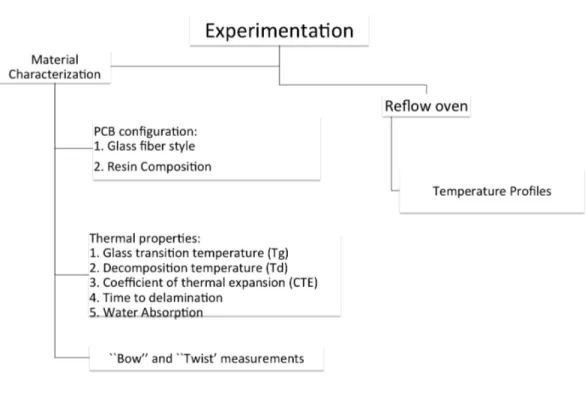
Based on literature review and the objectives established, an experimental plan was established as figure 5.1 shows.
Figure 5.1: Experimental procedure
5.1
Material Characterization
5.1.1
PCB configuration
The PCB material was provided by STACY CORPORATION, is a FR-4 laminate with seven layers of glass fiber, 40% brominated epoxy resin and two copper layers at the top and the bottom, as figure 5.2 shows.
Figure 5.2: PCB cross sectional view showing PCB ayers configuration
5.1.2
Thermal Properties
5.1. Material Characterization 35
Table 5.1: Thermal properties standards
Property Units Standard Equipment
Glass transition temperature oC IPC-TM-650 2.4.25 DSC Decomposition temperature oC IPC-TM-650 4.24.6 TGA Coefficient of thermal expansion “z” ppm/oC IPC-TM-650 2.4.24.5 TMA Coefficient of thermal expansion “x’ ppm/oC IPC-TM-650 2.4.24.5 TMA Coefficient of thermal expansion “y” ppm/oC IPC-TM-650 2.4.24.5 TMA
Time to delamination min IPC-TM-650 2.4.24.1 TMA
Water absorption % IPC-TM-650 2.6.2.1 Balance
Bow and twist % IPC-TM-650 2.4.22 c Gages, vernier
Figure 5.3: Specimens at different areas of PCB
The nominal material properties according to the supplier data sheet are listed in table 5.2.
Table 5.2: Material thermal properties
Property Units Value
Glass transition temperature oC 140
Decomposition temperature oC 310
Coefficient of thermal expansion before Tg ppm/oC 64 Coefficient of thermal expansion after Tg ppm/oC 300 % Coefficient of thermal expansion 50oC-260oC % 4.5
Time to delamination min 15
Water Absorption % 0.15
Figure 5.4: Preheating oven
Glass Transition Temperature (Tg)
The equipment used was a Netzch DSC pegasus F4 shown in figure 5.5. Specimens were prepared based on the IPC-TM-650 2.4.25 standard [19]. The test was run in an argon atmosphere, the temperature range was from 24oC to 170oC at 20oC/min of heating rate. Results were obtained by the procedure established in IPC-TM-650 2.4.25 standard [19]. Figure 5.10 shows the specimens mounted to obtain glass transition temperature, the dimensions were 4 mm x 2 mm and 22 mg approximately of weight.
Decomposition Temperature
Specimens were prepared based on the IPC-TM-650 4.24.6 standard [66]. The Dy-namic Mechanical Analysis (DMA) apparatus shown in figure 5.7 was used.
5.1. Material Characterization 37
Figure 5.5: DSC Netzch pegasus
Figure 5.6: Specimens to obtain glass transition temperature
of 10oC/min. Specimen mass vs temperature charts were recorded, Td is reached when the specimen loses 5% of it’s initial mass. Figure 5.8 shows decomposition temperature specimens, dimensions and weight are the same as for Tg specimens.
Coefficient of Thermal Expansion (CTE)
The thermal expansion coefficient is obtained based on IPC-TM-standard 350-2.4.25.5. The equipment used was a Thermo-mechanical Analyzer (TMA) as figure 5.9 shows.
Figure 5.7: Dynamic Mechanical Analysis (DMA)
Figure 5.8: Specimens to obtain decomposition temperature
Time to delamination
Time of delamination test was based on IPC-TM -650-2.4.24.1 standard [22], speci-mens dispeci-mensions are 6.5 mm x 6.5 mm, a preheated for 2 hours at 105oC was applied. The test started from room temperature to 260oC at a heating rate of 10oC/min, a isotherm was applied for 10 minutes at 260oC. The delamination time is when a irreversible change in thickness occurs during the isotherm. Dimensions and weight specimens are the same with CTE specimens ones.
Water Absorption
Water absorption test were based on IPC-TM-650 2.6.2.1 [67]. Scales “OMRUS” of figure 5.11a was used. Figure 5.11b shows the specimens were used, specimens di-mensions were 2 in x 2 cm and 9.11 gr average weight, then specimens were preheated at 105oC for two hours.
5.1. Material Characterization 39
Figure 5.9: TMA (Thermo Mechanical Analyzer)
Figure 5.10: Specimens to obtain coefficient of thermal expansion
distilled water for 24 hours. After 24 hours specimens mass was recorded and % of absorption water was obtained by the formula 2.3 explained in Chapter 2.
“Bow” and “twist”
In chapter 2 and 3 it was mentioned that there are different techniques to obtained PCB deformations, “Shadow Moir´e” is one of the most precisely technique, however, it was decide to obtained as IPC-TM-650 2.4.22 bow and twist (percentage) standard [26] stated, due to we don’t have the necessary equipment to use Shadow Moire technique, also its expensive, instead data collected approach a good approximation of the PCB deformations with gage devices and measurement instruments.
3 lots were analyzed, 10 PCB per lot, giving a total of 30 PCB’s. Thicknesses, sides and diagonals lengths were measured also they are required to use the formulas of “bow” and “twist” and determine the results.
(a) Balance
(b) % Absorption water speci-mens
Figure 5.11: Specimens water absorption performed
Figure 5.12: Device to obtain height of the PCB’s
5.2
Reflow Oven
5.2.1
Temperature Profiles
PCB was performed to obtain profiles temperature. Four thermocouples were placed along the PCB in order to collect temperature data, also it was considered to place thermocouples at 1cm from PCB surface to obtain environment temperature and determine if there are a mismatch among PCB areas as figure 5.13.
5.2. Reflow Oven 41
Figure 5.13: PCB to measure oven temperatures
Figure 5.14 is a standard profile temperature, Z1 to Z2 are preheated stages during the first 60 seconds approximately then a isothermal is applied from stage Z3 to the beginning of stage Z6, after the isotherm the peak temperature occurs in Z6 and Z7 during 60 seconds to ensure the melting point of solder paste and finally a cooling rate is applied in Z8 and Z9 stages.
Results and Discussion
This chapter shows the results obtained as follows:
• Glass transition temperature.
• Decomposition temperature.
• Coefficient of thermal expansion.
• Time to delamination.
• Absorption water.
• % “Bow” and % “twist”.
• Reflow oven.
6.1
Glass Transition Temperature (Tg)
It is important to mention that the specimens were tested before reflow process, no thermal load was applied before, except when the PCB was fabricated. Figure 6.1, figure 6.2 and figure 6.3 represents the results for top, middle and bottom areas, respectively.
6.1. Glass Transition Temperature (Tg) 43
Figure 6.1: Glass transition temperature chart top area
Figure 6.3: Glass transition temperature chart bottom area
Table 6.1 shows the values for the 3 areas.
Table 6.1: Glass transition temperature results for the 3 areas
Area Temperature (oC)
Top 138.48
Middle 138.6 Bottom 136.47 Average 137.85
6.1. Glass Transition Temperature (Tg) 45
Material thermal properties are different at elevated temperatures, “warpage” is originated due to thermal properties mismatch during reflow process, thermal conductivity are different between glass fiber, epoxy resin and copper. Table 6.2 shows the thermal conductivity of base materials, the difference between them is evident, glass fiber has the lowest value of thermal conductivity, whereas copper has 401 W
m·oC, that means, glass fiber restricted that heat flow and the copper allows the
heat transfer with more velocity that glass fiber and epoxy resin.
Table 6.2: Thermal conductivity of base materials [3]
Material Thermal Conductivity ( W m·oC)
Fiber Glass 0.04
Cobre 401
Epoxy resin 0.35
If we determined the heat transfer individually considering conduction heat trans-fer mechanism, values for base materials obtained individually are:
• Copper: 185,605.7 kW
• Epoxy resin: 52.018 kW
• Glass fiber: 6.89 kW
6.2
Decomposition Temperature (Td)
Decomposition temperature is when the material suffers irreversible changes. 2% and 5% of mass loss is recorded.
Figure 6.4, shows decomposition temperature of the three specimens, “x” axis represents temperature in degrees Celsius (◦C) and “y” axis the mass loss percentage.
Note that the three specimens have a mass loss at 300oC, approximately.
Figure 6.4: Decomposition temperature chart
To obtain more accurate results, specimen 1 and 2 data were fixed where mass loss occurs. Table 6.3 summarized the results.
Table 6.3: Specimens mass to obtain decomposition temperature
Specimen Initial mass %2 mass lost / %5 mass lost/ (gr) temperature (oC) temperature (oC)
1 12.43 12.18/294.87 11.80/299.20
2 33.01 32.34/300.28 30.72/302.29
Figure 6.5 corresponds the specimen 1 mass loss. 2% mass loss is at 294.87oC as the yellow point shows, also in figure 6.5 the red box indicates the 5% of mass loss which is 299.20oC.
6.2. Decomposition Temperature (Td) 47
Figure 6.5: Specimen 1 decomposition temperature chart
302.29oC for 5% mass loss.
Figure 6.6: Specimen 2 decomposition temperature chart
pre-sented. Also no full cured decrease decomposition temperature, in this case if the temperature is lower than traditional temperature (300oC) during reflow process the resin can be suffer a decomposition affecting the reliability of whole product.
6.3
Coefficient of Thermal Expansion
Coefficient of thermal expansion are presented as follows:
• Coefficient of thermal expansion results in the “x” axis.
• Coefficient of thermal expansion results in the “y” axis.
• Coefficient of thermal expansion results in the “z” axis.
6.3.1
Coefficient of Thermal Expansion in the “x” axis
Figure 6.7 shows the results of “x” axis at the top area, the behavior presented is a typical for glass fiber/epoxy resin laminate, change of direction is observed as yellow point marks.
6.3. Coefficient of Thermal Expansion 49
Figure 6.8 shows the results of the coefficient of thermal expansion in the axis “x”, but at the middle area. Clearly, the behavior is quite different in comparison with figure 6.7, as yellow point indicates, when temperature approaches to the glass transition a material contraction is observed, then at 140oC the material expansion continues linearly.
Figure 6.8: Coefficient of thermal expansion “x” axis at middle area
Figure 6.9 shows the results of coefficient of thermal expansion at the bottom. The behavior is similar to the coefficient of thermal expansion of the top area, yellow point indicates the change in specimen thickness at 130.9oC.
Figure 6.9: Coefficient of thermal expansion “x” axis at bottom area
This change of thickness is due to during the test a force of µN is applied when the specimen reaches a temperature close to the glass transition, the material becomes in a glassy state and with the force applied the material is contracted, this temperature is around 129oC. The contraction observed can cause undesirable epoxy resin flow.
Two coefficients of thermal expansion are obtained, one before and one after the glass transition temperature, two points are selected, before the transition “A” and “B” temperature and thicknesses are recorded and substituted in the formula 2.1:
For the thermal expansion coefficient after the glass transition temperature same procedure is repeated, except that two different points after the transition must be selected. Table 6.4 summarizes “x” axis results, thermal expansion coefficients and % thermal expansion at the three areas are showed.
Table 6.4: Results at 3 areas for “x” axis
Area thermal expansion(%) CTE before Tg (ppm/oC) CTE after Tg (ppm/oC)
Top 0.17 14.81 7.12
Middle 0.16 14.90 6.92
Bottom 0.18 15.30 9.00
It is observed bottom area presents an % expansion of 0.18% and the thermal expansion coefficients obtained were 15.30 ppm/oC and 9.00 ppm/oC before and after glass transition temperature, respectively.
Top and middle area values are similar, but the difference between top and bottom area is 0.49ppm /oC for CTE before the glass transition temperature and 1.88 ppm /oC after glass transition temperature.
6.3.2
Coefficient of Thermal Expansion in the “y” axis
Figure 6.10 represented the coefficient thermal expansion at top area in “y” axis, the red point marks a material contraction at 127.75oC close to the glass transition temperature, after tansition the material continue it’s deformation linearly.
6.3. Coefficient of Thermal Expansion 51
Figure 6.10: Coefficient of thermal expansion “y” axis at top area
Figure 6.11: Coefficient of thermal expansion “y” axis at middle area
Figure 6.12 represents the results of “y” at the bottom, red point marks the contraction at 130.20oC.
Coefficient of thermal expansion in “y” axis differs between top and middle area with bottom area. Table 6.5 group the results of thermal expansion coefficient per-centages and the thermal expansion coefficients in “y” axis for three three areas.
Figure 6.12: Coefficient of thermal expansion “y” axis at bottom area
Table 6.5: Results at 3 areas for “y” axis
Area % thermal expansion CTE before Tg CTE after Tg
Top 0.119486757 13.29 1.53
Middle 0.117747654 13.08 2.11
Bottom 0.157205569 13.77 7.12
6.3. Coefficient of Thermal Expansion 53
6.3.3
Coefficient of Thermal Expansion in the “z” axis
In industry, “z” axis is the major concern where deformations are generated and “warpage” is observed. Results of the coefficient of expansion and thermal expansion percentage in “z” axis were analyzed. Figure 6.13 shows the results of the coefficient of thermal expansion in the axis “z” at the top. The behavior is normal according with the standard [71], near the glass transition temperature an expansion is observed at 136.79oC, after transition material continues it’s lineal expansion at a similar rate before the glass transition temperature.
Figure 6.13: Coefficient of thermal expansion “z” axis at top area
Figure 6.14: Coefficient of thermal expansion “z” axis at middle area
Figure 6.15: Coefficient of thermal expansion “z” axis at bottom area
Figure 6.15 represents the coefficient of thermal expansion at the bottom, the results are similar with the top area, the transition at the bottom occurs at 134.82oC, these values are similar to those reported in the literature so. Table 6.6 shows the thermal expansion coefficients before and after the glass transition temperature and thermal expansion percentages for “z” axis.
Table 6.6: Results at 3 areas for “z” axis
Area % thermal expansion CTE before Tg CTE after Tg
Top 1,74 75.12 283.15
Middle 5.27 353.82 327.68
Bottom 1.58 61.19 285.14
CTE’s values for “z” axis are in a range of 50-70 ppm/oC before glass transition temperature [21], results at the middle area are 353.82 this value is higher, it is speculated that there is a concentration of heat, the heterogeneity in that area is predominant, copper, resin and glass fiber distribution is poor, generating thermal stresses and deformations along the axis, one of the reasons is that the resin expands with a higher rate of deformation in comparison with glass fiber.
6.3. Coefficient of Thermal Expansion 55
Table 6.7: CTE results at 3 areas
Area Axis CTE before tg CTE after tg
“x” 14.81 7.12
Top “y” 13.29 1.53
“z” 75.12 283.15
“x” 14.90 7.12
Middle “y” 13.08 2.11
“z” 353.82 327.68
“x” 15.30 9.00
Bottom “y” 13.77 7.12
“z” 61.19 285.14
6.4
Time to Delamination
Figure 6.16 is a thickness versus temperature chart of specimen took from the top area. Blue line corresponds the thickness and the red line the temperature, inten-tionally temperature above 260oC was raised in order to generate delaminations and explain it. Green box represents the constant temperature and bracket in black in-dicates a first elevation in thickness at 25 minutes. First peak represents a reversible deformation where the material expands and contracts, however, as the isotherm con-tinues, peaks are generate,this means that the material is undergoing delamination and material suffers irreversible changes causing material disintegration.
Figure 6.16: Time to delamination results at the top
6.4. Time to Delamination 57
Figure 6.17: Time to delamination results at the middle
Figure 6.18: Time to delamination results at the bottom
Concluding specimens tested for time to delamination passed the test with no delaminations presented.
6.5
Water Absorption
Acceptable values is 0.15% according with material supplier date sheet. Table 6.8 shows the percentages obtained.
Table 6.8: Water absorption results
Specimen Mass before (gr) Mass after (gr) % absorption water
1 8.45 8.47 0.17
2 8.80 8.81 0.13
3 9.37 9.39 0.19
4 9.81 9.83 0.16
Specimens 1, 2 and 4 are slightly above with values of 0.17%, 0.13% and 0.16%, respectively, in the other hand specimen 3 with a value of % water absorption of 0.19%. This value is related with manufacturing laminated defects such as: in-correct resin/fiber impregnation, poor curing, existence of gaps, micro fractures, delaminations and weak fiberglass and epoxy resin interphase.
6.6
Bow and Twist Measurement
This section presents the “bow” and “twist” results as follows:
1. PCB “bow” after first reflow
2. PCB “bow” after second reflow
3. PCB “twist” after first reflow
4. PCB “twist” after second reflow
Initial data recorded are presented in appendix B.
6.6.1
PCB “bow” after first reflow
6.6. Bow and Twist Measurement 59
Substituting values in equation 6.1 and taking “L” values from table B, “bow” after first reflow at each side were obtained the results are shown in figure 6.19. Data is presented in appendix C.1
Figure 6.19: PCB “bow” results after first reflow
%Bow = R
L(100) (6.1)
According with figure 6.19 “BC” and “DA” sides presents higher elevations. “BC” side present a range of deformations from 0.2 mm (PCB #22) to 1.86 mm (PCB #26). PCB mean deformation in “BC” side is 1.26 mm. In the other hand “DA” side have a range of deformations from 0.07 mm (PCB #22) to 1.79 mm (PCB #26). PCB mean deformation in “DA” side is 1.15 mm.
Sides “AB” and “CD” presents less deformations as figure 6.19 shown, it is evident that the elevations are very similar for all PCB’s. “AB” side has a deformation range from -0.05 mm (PCB #18) to 0.68 mm (PCB #4), the mean deformation of “AB” side is 0.19 mm. For “CD” side the deformation range is from -0.06 mm to 0.66 mm and it’s mean deformation is 0.30 mm.
Concluding the sides susceptible to thermo-mechanical stresses are “BC” and “DA” sides causing higher values of “bow” after first reflow in comparison with “AB” and “CD” sides, which are more stable.


![Table 2.1: PCB’s classification [3].](https://thumb-us.123doks.com/thumbv2/123dok_es/6209731.186360/17.918.256.724.603.930/table-pcb-s-classification.webp)

![Table 2.3 shows the traditional arrangements available [8]. Table 2.3: Traditional woven glass fabric styles [8] Style Glass thickness (mm) Weight (gsm) Threads per cm](https://thumb-us.123doks.com/thumbv2/123dok_es/6209731.186360/21.918.238.736.184.339/table-traditional-arrangements-available-traditional-thickness-weight-threads.webp)