ANALOG-DIGITAL CONVERSION
1. Data Converter History
2. Fundamentals of Sampled Data Systems
3. Data Converter Architectures
4. Data Converter Process Technology
5. Testing Data Converters
6. Interfacing to Data Converters
7. Data Converter Support Circuits
8. Data Converter Applications
9. Hardware Design Techniques
9.1 Passive Components
9.2 PC Board Design Issues
9.3 Analog Power Supply Systems
9.4 Overvoltage Protection
9.5 Thermal Management
9.6 EMI/RFI Considerations
9.7 Low Voltage Logic Interfacing
9.8 Breadboarding and Prototyping
CHAPTER 9
HARDWARE DESIGN TECHNIQUES
This chapter, one of the longer of those within the book, deals with topics just as important as all of those basic circuits immediately surrounding the data converter, discussed earlier. The chapter deals with various and sundry circuit/system issues which fall under the guise of system hardware design techniques. In this context, the design techniques may be all those support items surrounding a data converter, excluding the data converter itself. This includes issues of passive components, printed circuit design, power supply systems, protection of linear devices against overvoltage and thermal effects, EMI/RFI issues, high speed logic considerations, and finally, simulation,
breadboarding and prototyping. Some of these topics aren't directly involved in the actual signal path of a design, but they are every bit as important as choosing the correct device and surrounding circuit values.
Remote sensing and signal conditioning is such a vital part of data conversion that a considerable amount of discussion is given to topics such as overvoltage protection, cable driving, shielding, and receiving—where the remote interface is often with op amps and instrumentation amplifiers. Much of this material has been extracted from a companion publication by Walter G. Jung: Op Amp Applications, Analog Devices, 2002.
SECTION 9.1: PASSIVE COMPONENTS
James Bryant, Walt Jung, Walt Kester
Introduction
When designing with data converters, op amps, and other precision analog devices, it is critical that users avoid the pitfall of poor passive component choice. In fact, the wrong passive component can derail even the best op amp or data converter application. This section includes discussion of some basic traps of choosing passive components for op amp and data converter applications.
So, you've spent good money for a precision op amp or data converter, only to find that, when plugged into your board, the device doesn't meet spec. Perhaps the circuit suffers from drift, poor frequency response, and oscillations—or simply doesn't achieve expected accuracy. Well, before you blame the device, you should closely examine your passive components—including capacitors, resistors, potentiometers, and yes, even the printed circuit boards. In these areas, subtle effects of tolerance, temperature, parasitics, aging, and user assembly procedures can unwittingly sink your circuit. And all too often these effects go unspecified (or underspecified) by passive component manufacturers.
Consider the case of a 12-bit DAC, where ½ LSB corresponds to 0.012% of full scale, or only 122 ppm. A host of passive component phenomena can accumulate errors far exceeding this! But, buying the most expensive passive components won't necessarily solve your problems either. Often, a correct 25-cent capacitor yields a better-performing, more cost-effective design than a premium-grade part. With a few basics, understanding and analyzing passive components may prove rewarding, albeit not easy.
Capacitors
Most designers are generally familiar with the range of capacitors available. But the mechanisms by which both static and dynamic errors can occur in precision circuit designs using capacitors are sometimes easy to forget, because of the tremendous variety of types available. These include dielectrics of glass, aluminum foil, solid tantalum and tantalum foil, silver mica, ceramic, Teflon, and the film capacitors, including polyester, polycarbonate, polystyrene, and polypropylene types. In addition to the traditional leaded packages, many of these are now also offered in surface mount styles.
Figure 9.1 is a workable model of a non-ideal capacitor. The nominal capacitance, C, is shunted by a resistance RP, which represents insulation resistance or leakage. A second resistance, RS—equivalent series resistance, or ESR,—appears in series with the capacitor and represents the resistance of the capacitor leads and plates.
Figure 9.1: A Non-Ideal Capacitor Equivalent Circuit Includes Parasitic Elements
Note that capacitor phenomena aren't that easy to isolate. The matching of phenomena and models is for convenience in explanation. Inductance, L—the equivalent series inductance, or ESL—models the inductance of the leads and plates. Finally, resistance RDA and capacitance CDA together form a simplified model of a phenomenon known as
dielectric absorption, or DA. It can ruin fast and slow circuit dynamic performance. In a real capacitor RDA and CDA extend to include multiple parallel sets. These parasitic RC elements can act to degrade timing circuits substantially, and the phenomenon is discussed further below.
C RP
RS
(ESR)
RDA CDA
Dielectric Absorption
Dielectric absorption, which is also known as "soakage" and sometimes as "dielectric hysteresis"—is perhaps the least understood and potentially most damaging of various capacitor parasitic effects. Upon discharge, most capacitors are reluctant to give up all of their former charge, due to this memory consequence.
Figure 9.2 illustrates this effect. On the left of the diagram, after being charged to the source potential of V volts at time to, the capacitor is shorted by the switch S1 at time t1, discharging it. At time t2, the capacitor is then open-circuited; a residual voltage slowly builds up across its terminals and reaches a nearly constant value. This error voltage is due to DA, and is shown in the right figure, a time/voltage representation of the
charge/discharge/recovery sequence. Note that the recovered voltage error is proportional to both the original charging voltage V, as well as the rated DA for the capacitor in use.
Figure 9.2: A Residual Open-Circuit Voltage After Charge/Discharge Characterizes Capacitor Dielectric Absorption
Standard techniques for specifying or measuring dielectric absorption are few and far between. Measured results are usually expressed as the percentage of the original charging voltage that reappears across the capacitor. Typically, the capacitor is charged for a long period, then shorted for a shorter established time. The capacitor is then allowed to recover for a specified period, and the residual voltage is then measured (see Reference 8 for details). While this explanation describes the basic phenomenon, it is important to note that real-world capacitors vary quite widely in their susceptibility to this error, with their rated DA ranging from well below to above 1%, the exact number being a function of the dielectric material used.
In practice, DA makes itself known in a variety of ways. Perhaps an integrator refuses to reset to zero, a voltage-to-frequency converter exhibits unexpected nonlinearity, or a sample-hold amplifier (SHA) exhibits varying errors. This last manifestation can be particularly damaging in a data-acquisition system, where adjacent channels may be at voltages which differ by nearly full scale, as shown below.
Figure 9.3 illustrates the case of DA error in a simple SHA. On the left, switches S1 and S2 represent an input multiplexer and SHA switch, respectively. The multiplexer output voltage is VX, and the sampled voltage held on C is VY, which is buffered by the op amp for presentation to an ADC. As can be noted by the timing diagram on the right, a DA error voltage, ∈, appears in the hold mode, when the capacitor is effectively open circuit.
S1
C VO
V t1
t0
t2
t2 t1 t0
V VO
This voltage is proportional to the difference of voltages V1 and V2, which, if at opposite extremes of the dynamic range, exacerbates the error. As a practical matter, the best solution for good performance in terms of DA in a SHA is to use only the best capacitor.
Figure 9.3: Dielectric Absorption Induces Errors in SHA Applications
The DA phenomenon is a characteristic of the dielectric material itself, although inferior manufacturing processes or electrode materials can also affect it. DA is specified as a percentage of the charging voltage. It can range from a low of 0.02% for Teflon, polystyrene, and polypropylene capacitors, up to a high of 10% or more for some electrolytics. For some time frames, the DA of polystyrene can be as low as 0.002%. Common high-K ceramics and polycarbonate capacitor types display typical DA on the order of 0.2%, it should be noted this corresponds to ½ LSB at only 8 bits! Silver mica, glass, and tantalum capacitors typically exhibit even larger DA, ranging from 1.0% to 5.0%, with those of polyester devices falling in the vicinity of 0.5%. As a rule, if the capacitor spec sheet doesn't specifically discuss DA within your time frame and voltage range, exercise caution! Another type with lower specified DA is likely a better choice. DA can produce long tails in the transient response of fast-settling circuits, such as those found in high-pass active filters or ac amplifiers. In some devices used for such
applications, Figure 9.1's RDA-CDA model of DA can have a time constant of
milliseconds. Much longer time constants are also quite usual. In fact, several paralleled RDA-CDA circuit sections with a wide range of time constants can model some devices. In fast-charge, fast-discharge applications, the behavior of the DA mechanism resembles "analog memory"; the capacitor in effect tries to remember its previous voltage.
In some designs, you can compensate for the effects of DA if it is simple and easily characterized, and you are willing to do custom tweaking. In an integrator, for instance, the output signal can be fed back through a suitable compensation network, tailored to cancel the circuit equivalent of the DA by placing a negative impedance effectively in parallel. Such compensation has been shown to improve SH circuit performance by factors of 10 or more (Reference 6).
V1
∈ = (V1-V2) DA
V2 VX
VY
S2 OPEN
CLOSED S1
C S2
VX
VY V1
V2
V3
VN
Capacitor Parasitics and Dissipation Factor
In Figure 9.1, a capacitor's leakage resistance, RP, the effective series resistance, RS, and effective series inductance, L, act as parasitic elements, which can degrade an external circuit's performance. The effects of these elements are often lumped together and defined as a dissipation factor, or DF.
A capacitor's leakage is the small current that flows through the dielectric when a voltage is applied. Although modeled as a simple insulation resistance (RP) in parallel with the capacitor, the leakage actually is nonlinear with voltage. Manufacturers often specify leakage as a megohm-microfarad product, which describes the dielectric's self-discharge time constant, in seconds. It ranges from a low of 1 second or less for high-leakage capacitors, such as electrolytic devices, to the 100s of seconds for ceramic capacitors. Glass devices exhibit self-discharge time-constants of 1,000 or more; but the best leakage performance is shown by Teflon and the film devices (polystyrene, polypropylene), with time constants exceeding 1,000,000 megohm-microfarads. For such a device, external leakage paths—created by surface contamination of the device's case or in the associated wiring or physical assembly—can overshadow the internal dielectric-related leakage. Effective series inductance, ESL (Figure 9.1, again) arises from the inductance of the capacitor leads and plates, which, particularly at the higher frequencies, can turn a capacitor's normally capacitive reactance into an inductive reactance. Its magnitude strongly depends on construction details within the capacitor. Tubular wrapped-foil devices display significantly more lead inductance than molded radial-lead
configurations. Multilayer ceramic (MLC) and film-type devices typically exhibit the lowest series inductance, while ordinary tantalum and aluminum electrolytics typically exhibit the highest. Consequently, standard electrolytic types, if used alone, usually prove insufficient for high-speed local bypassing applications. Note however that there also are more specialized aluminum and tantalum electrolytics available, which may be suitable for higher speed uses, however, localized bypassing is still recommended. These are the types generally designed for use in switch-mode power supplies, which are covered more completely in a following section.
Manufacturers of capacitors often specify effective series impedance by means of impedance-versus-frequency plots. Not surprisingly, these curves show graphically a predominantly capacitive reactance at low frequencies, with rising impedance at higher frequencies because of the effect of series inductance.
Dissipation factor often varies as a function of both temperature and frequency.
Capacitors with mica and glass dielectrics generally have DF values from 0.03% to 1.0%. For ceramic devices, DF ranges from a low of 0.1 % to as high as 2.5% at room
temperature. And electrolytics usually exceed even this level. The film capacitors are the best as a group, with DFs of less than 0.1 %. Stable-dielectric ceramics, notably the NP0 (also called COG) types, have DF specs comparable to films (more below).
Tolerance, Temperature, and Other Effects
In general, precision capacitors are expensive and—even then—not necessarily easy to buy. In fact, choice of capacitance is limited both by the range of available values, and also by tolerances. In terms of size, the better performing capacitors in the film families tend to be limited in practical terms to 10 µF or less (for dual reasons of size and expense). In terms of low value tolerance, ±1% is possible for NP0 ceramic and some film devices, but with possibly unacceptable delivery times. Many film capacitors can be made available with tolerances of less than ±1%, but on a special order basis only. Most capacitors are sensitive to temperature variations. DF, DA, and capacitance value are all functions of temperature. For some capacitors, these parameters vary
approximately linearly with temperature, in others they vary quite nonlinearly. Although it is usually not important for SHA applications, an excessively large temperature coefficient (TC, measured in ppm/°C) can prove harmful to the performance of precision integrators, voltage-to-frequency converters, and oscillators. NP0 ceramic capacitors, with TCs as low as 30 ppm/°C, are the best for stability, with polystyrene and
polypropylene next best, with TCs in the 100-200 ppm/°C range. On the other hand, when capacitance stability is important, one should stay away from types with TCs of more than a few hundred ppm/°C, or in fact any TC which is nonlinear.
A capacitor's maximum working temperature should also be considered, in light of the expected environment. Polystyrene capacitors, for instance, melt near 85°C, compared to Teflon's ability to survive temperatures up to 200°C.
Sensitivity of capacitance and DA to applied voltage, expressed as voltage coefficient, can also hurt capacitor performance within a circuit application. Although capacitor manufacturers don't always clearly specify voltage coefficients, the user should always consider the possible effects of such factors. For instance, when maximum voltages are applied, some high-K ceramic devices can experience a decrease in capacitance of 50% or more. This is an inherent distortion producer, making such types unsuitable for signal path filtering, for example, and better suited for supply bypassing. Interestingly, NP0 ceramics, the stable dielectric subset from the wide range of available ceramics, do offer good performance with respect to voltage coefficient.
Assemble Critical Components Last
The designer's worries don't end with the design process. Some common printed circuit assembly techniques can prove ruinous to even the best designs. For instance, some commonly used cleaning solvents can infiltrate certain electrolytic capacitors—those with rubber end caps are particularly susceptible. Even worse, some of the film capacitors, polystyrene in particular, actually melt when contacted by some solvents. Rough handling of the leads can damage still other capacitors, creating random or even intermittent circuit problems. Etched-foil types are particularly delicate in this regard. To avoid these difficulties it may be advisable to mount especially critical components as the last step in the board assembly process—if possible.
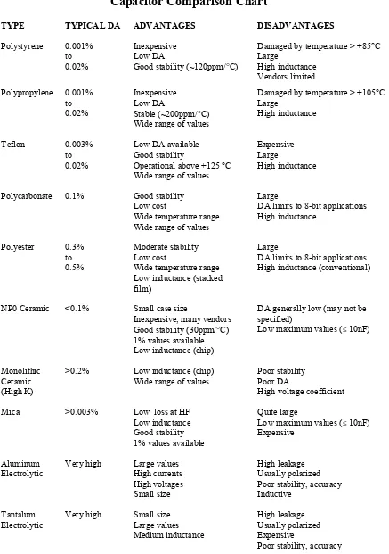
Table 9.1 summarizes selection criteria for various capacitor types, arranged roughly in order of decreasing DA performance. In a selection process, the general information of this table should be supplemented by consultation of current vendor's catalog information (see References at end of section).
Designers should also consider the natural failure mechanisms of capacitors. Metallized film devices, for instance, often self-heal. They initially fail due to conductive bridges that develop through small perforations in the dielectric film. But, the resulting fault currents can generate sufficient heat to destroy the bridge, thus returning the capacitor to normal operation (at a slightly lower capacitance). Of course, applications in
high-impedance circuits may not develop sufficient current to clear the bridge, so the designer must be wary here.
Tantalum capacitors also exhibit a degree of self-healing, but—unlike film capacitors— the phenomenon depends on the temperature at the fault location rising slowly.
Therefore, tantalum capacitors self-heal best in high impedance circuits which limit the surge in current through the capacitor's defect. Use caution therefore, when specifying tantalums for high-current applications.
Table 9.1
Capacitor Comparison Chart
TYPE TYPICAL DA ADVANTAGES DISADVANTAGES
Polystyrene 0.001% to
0.02%
Inexpensive Low DA
Good stability (~120ppm/°C)
Damaged by temperature > +85°C Large High inductance Vendors limited Polypropylene 0.001% to 0.02% Inexpensive Low DA Stable (~200ppm/°C) Wide range of values
Damaged by temperature > +105°C Large
High inductance
Teflon 0.003% to
0.02%
Low DA available Good stability
Operational above +125 °C Wide range of values
Expensive Large
High inductance
Polycarbonate 0.1% Good stability Low cost
Wide temperature range Wide range of values
Large
DA limits to 8-bit applications High inductance Polyester 0.3% to 0.5% Moderate stability Low cost
Wide temperature range Low inductance (stacked film)
Large
DA limits to 8-bit applications High inductance (conventional)
NP0 Ceramic <0.1% Small case size
Inexpensive, many vendors Good stability (30ppm/°C) 1% values available Low inductance (chip)
DA generally low (may not be specified)
Low maximum values (≤ 10nF)
Monolithic Ceramic (High K)
>0.2% Low inductance (chip)
Wide range of values Poor stability Poor DA
High voltage coefficient
Mica >0.003% Low loss at HF Low inductance Good stability 1% values available
Quite large
Low maximum values (≤ 10nF) Expensive
Aluminum Electrolytic
Very high Large values High currents High voltages Small size
High leakage Usually polarized Poor stability, accuracy Inductive
Tantalum Electrolytic
Very high Small size Large values Medium inductance
High leakage Usually polarized Expensive
Resistors and Potentiometers
Designers have a broad range of resistor technologies to choose from, including carbon composition, carbon film, bulk metal, metal film, and both inductive and non-inductive wire-wound types. As perhaps the most basic—and presumably most trouble-free—of components, resistors are often overlooked as error sources in high performance circuits. Yet, an improperly selected resistor can subvert the accuracy of a 12-bit design by
developing errors well in excess of 122 ppm (½ LSB). When did you last read a resistor data sheet? You'd be surprised what can be learned from an informed review of data.
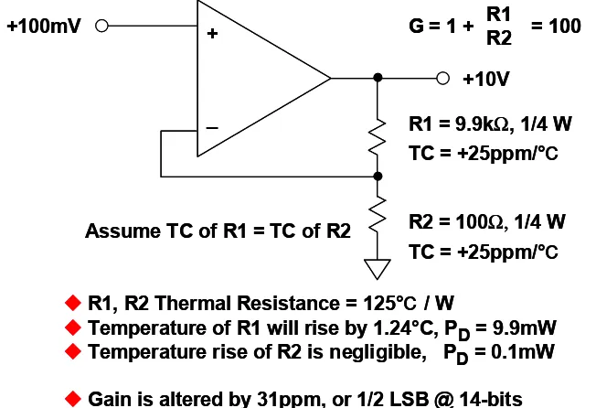
Figure 9.4: Mismatched Resistor TCs Can Induce Temperature-Related Gain Errors
Consider the simple circuit of Figure 9.4, showing a non-inverting op amp where the 100× gain is set by R1 and R2. The TCs of these two resistors are a somewhat obvious source of error. Assume the op amp gain errors to be negligible, and that the resistors are perfectly matched to a 99/1 ratio at +25ºC. If, as noted, the resistor TCs differ by only 25 ppm/ºC, the gain of the amplifier changes by 250 ppm for a 10ºC temperature change. This is about a 1 LSB error in a 12-bit system, and a major disaster in a 16-bit system. Temperature changes, however, can limit the accuracy of the Figure 9.4 amplifier in several ways. In this circuit (as well as many op amp circuits with component-ratio defined gains), the absolute TC of the resistors is less important—as long as they track one another in ratio. But even so, some resistor types simply aren't suitable for precise work. For example, carbon composition units—with TCs of approximately
1,500 ppm/°C, won't work. Even if the TCs could be matched to an unlikely 1%, the resulting 15-ppm/°C differential still proves inadequate—an 8°C shift creates a 120-ppm error.
Many manufacturers offer metal film and bulk metal resistors, with absolute TCs ranging between ±1 and ±100 ppm/°C. Beware, though; TCs can vary a great deal, particularly
R1 = 9.9kΩ, 1/4 W TC = +25ppm/°
c
R2 = 100Ω, 1/4 W TC = +50ppm/°
c
G = 1 + R1R2 = 100
Temperature change of 10°C causes gain change of 250ppm
This is 1LSB in a 12-bit system and a disaster in a 16-bit system +
_ R1 = 9.9kΩ, 1/4 W TC = +25ppm/°
c
R2 = 100Ω, 1/4 W TC = +50ppm/°
c
G = 1 + R1R2 = 100
Temperature change of 10°C causes gain change of 250ppm
This is 1LSB in a 12-bit system and a disaster in a 16-bit system +
among discrete resistors from different batches. To avoid this problem, more expensive matched resistor pairs are offered by some manufacturers, with temperature coefficients that track one another to within 2 to 10 ppm/°C. Low-priced thin-film networks have good relative performance and are widely used.
Figure 9.5: Uneven Power Dissipation Between Resistors With Identical TCs Can Also Introduce Temperature-Related Gain Errors
Suppose, as shown in Figure 9.5, R1 and R2 are ¼W resistors with identical 25-ppm/ºC TCs. Even when the TCs are identical, there can still be significant errors! When the signal input is zero, the resistors dissipate no heat. But, if it is 100 mV, there is 9.9 V across R1, which then dissipates 9.9 mW. It will experience a temperature rise of 1.24ºC (due to a 125ºC/W, ¼W resistor thermal resistance). This 1.24ºC rise causes a resistance change of 31 ppm, and thus a corresponding gain change. But R2, with only 100 mV across it, is only heated a negligible 0.0125ºC. The resulting 31-ppm net gain error represents a fullscale error of ½ LSB at 14-bits, and is a disaster for a 16-bit system. Even worse, the effects of this resistor self-heating also create easily calculable
nonlinearity errors. In the Figure 9.5 example, with ½ the voltage input, the resulting self-heating error is only 15 ppm. In other words, the stage gain is not constant at ½ and full-scale (nor is it so at other points), as long as uneven temperature shifts exist between the gain-determining resistors. This is by no means a worst-case example; physically smaller resistors would give worse results, due to higher associated thermal resistance.
These, and similar errors, are avoided by selecting critical resistors that are accurately matched for both value and TC, are well derated for power, and have tight thermal coupling between those resistors were matching is important. This is best achieved by using a resistor network on a single substrate—such a network may either be within an IC, or it may be a separately packaged thin-film resistor network.
R1 = 9.9kΩ, 1/4 W TC = +25ppm/°
c
R2 = 100Ω, 1/4 W TC = +25ppm/°
c
+100mV G = 1 + R1
R2 = 100
+10V
R1, R2 Thermal Resistance = 125°
c
/ WTemperature of R1 will rise by 1.24°C, PD= 9.9mW Temperature rise of R2 is negligible, PD= 0.1mW
Gain is altered by 31ppm, or 1/2 LSB @ 14-bits +
_
Assume TC of R1 = TC of R2
R1 = 9.9kΩ, 1/4 W TC = +25ppm/°
c
R2 = 100Ω, 1/4 W TC = +25ppm/°
c
+100mV G = 1 + R1
R2 = 100 G = 1 + R1
R2 = 100
+10V
R1, R2 Thermal Resistance = 125°
c
/ WTemperature of R1 will rise by 1.24°C, PD= 9.9mW Temperature rise of R2 is negligible, PD= 0.1mW
Gain is altered by 31ppm, or 1/2 LSB @ 14-bits +
_
[image:12.612.127.453.130.353.2]When the circuit resistances are very low (≤10 Ω), interconnection stability also becomes important. For example, while often overlooked as an error, the resistance TC of typical copper wire or printed circuit traces can add errors. The TC of copper is typically ~3,900 ppm/°C. Thus a precision 10-Ω, 10-ppm/°C wirewound resistor with 0.1 Ω of copper interconnect effectively becomes a 10.1-Ω resistor with a TC of nearly 50 ppm/°C.
One final consideration applies mainly to designs that see widely varying ambient temperatures: a phenomenon known as temperature retrace describes the change in resistance which occurs after a specified number of cycles of exposure to low and high ambients with constant internal dissipation. Temperature retrace can exceed 10 ppm/°C, even for some of the better thin-film components.
In summary, to design resistance-based circuits for minimum temperature-related errors, consider the points noted in Figure 9.6 (along with their cost).
Figure 9.6: A Number of Points are Important Towards Minimizing Temperature-Related Errors in Resistors
Resistor Parasitics
Resistors can exhibit significant levels of parasitic inductance or capacitance, especially at high frequencies. Manufacturers often specify these parasitic effects as a reactance error, in % or ppm, based on the ratio of the difference between the impedance magnitude and the dc resistance, to the resistance, at one or more frequencies.
Wirewound resistors are especially susceptible to difficulties. Although resistor
manufacturers offer wirewound components in either normal or noninductively wound form, even noninductively wound resistors create headaches for designers. These resistors still appear slightly inductive (of the order of 20 µH) for values below 10 kΩ. Above 10 kΩ the same style resistors actually exhibit 5 pF of shunt capacitance. These parasitic effects can raise havoc in dynamic circuit applications. Of particular concern are applications using wirewound resistors with values greater than 10 kΩ. Here it isn't uncommon to see peaking, or even oscillation. These effects become more evident at low-kHz frequency ranges.
Closely match resistance TCs.
Use resistors with low absolute TCs.
Use resistors with low thermal resistance (higher power ratings, larger cases).
Tightly couple matched resistors thermally (use standard common-substrate networks).
Even in low-frequency circuit applications, parasitic effects in wirewound resistors can create difficulties. Exponential settling to 1 ppm may take 20 time constants or more. The parasitic effects associated with wirewound resistors can significantly increase net circuit settling time to beyond the length of the basic time constants.
Unacceptable amounts of parasitic reactance are often found even in resistors that aren't wirewound. For instance, some metal-film types have significant interlead capacitance, which shows up at high frequencies. In contrast, when considering this end-to-end capacitance, carbon resistors do the best at high frequencies.
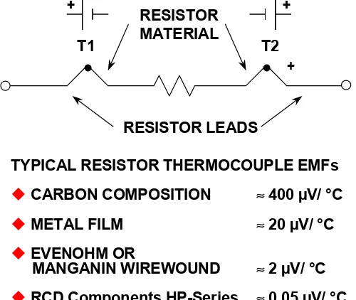
Thermoelectric Effects
Another more subtle problem with resistors is the thermocouple effect, also sometimes referred to as thermal EMF. Wherever there is a junction between two different metallic conductors, a thermoelectric voltage results. The thermocouple effect is widely used to measure temperature. However, in any low level precision op amp circuit it is also a potential source of inaccuracy, since wherever two different conductors meet, a
thermocouple is formed (whether we like it or not). In fact, in many cases, it can easily produce the dominant error within an otherwise precision circuit design.
Parasitic thermocouples will cause errors when and if the various junctions forming the parasitic thermocouples are at different temperatures. With two junctions present on each side of the signal being processed within a circuit, by definition we have formed at least one thermocouple pair. If the two junctions of this thermocouple pair are at different temperatures, there will be a net temperature dependent error voltage produced.
Conversely, if the two junctions of a parasitic thermocouple pair are kept at an identical temperature, then the net error produced will be zero, as the voltages of the two
thermocouples effectively will be canceled.
This is a critically important point, since in practice we cannot avoid connecting
dissimilar metals together to build an electronic circuit. But, what we can do is carefully control temperature differentials across the circuit, so such that the undesired
thermocouple errors cancel one another.
The effect of such parasitics is very hard to avoid. To understand this, consider a case of making connections with copper wire only. In this case, even a junction formed by
different copper wire alloys can have a thermoelectric voltage which is a small fraction of 1 µV/ºC! And, taking things a step further, even such apparently benign components as resistors contain parasitic thermocouples, with potentially even stronger effects.
Figure 9.7: Every Resistor Contains Two Thermocouples, Formed Between the Leads and Resistance Element
Note that these thermocouple effects are relatively unimportant for ac signals. Even for dc-only signals, they will nicely cancel one another, if, as noted above, the entire resistor is at a uniform temperature. However, if there is significant power dissipation in a resistor, or if its orientation with respect to a heat source is non-symmetrical, this can cause one of its ends to be warmer than the other, causing a net thermocouple error voltage. Using ordinary metal film resistors, an end-to-end temperature differential of 1ºC causes a thermocouple voltage of about 20 µV. This error level is quite significant
compared to the offset voltage drift of a precision op amp like the OP177, and extremely significant when compared to chopper-stabilized op amps, with their drifts of <1 µV/°C.
Figure 9.8: The Effects of Thermocouple EMFs Generated by Resistors can be Minimized by Orientation that Equalizes the End Temperatures
Figure 9.8 shows how resistor orientation can make a difference in the net thermocouple voltage. In the left diagram, standing the resistor on end in order to conserve board space will invariably cause a temperature gradient across the resistor, especially if it is
dissipating any significant power. In contrast, placing the resistor flat on the PC board as shown at the right will generally eliminate the gradient. An exception might occur, if
TYPICAL RESISTOR THERMOCOUPLE EMFs
CARBON COMPOSITION ≈ 400 µV/ °C
METAL FILM ≈ 20 µV/ °C
EVENOHM OR
MANGANIN WIREWOUND ≈ 2 µV/ °C
RCD Components HP-Series ≈ 0.05 µV/ °C RESISTOR
MATERIAL
RESISTOR LEADS
T1 T2
+ +
+ ++
∆T
WRONG RIGHT
∆T
[image:15.612.198.448.62.273.2]there is end-to-end resistor airflow. For such cases, orienting the resistor axis
perpendicular to the airflow will minimize this source of error, since this tends to force the resistor ends to the same temperature.
Note that this line of thinking should be extended, to include orientation of resistors on a vertically mounted PC board. In such cases, natural convection air currents tend to flow upward across the board. Again, the resistor thermal axis should be perpendicular to convection, to minimize thermocouple effects. With tiny surface mount resistors, the thermocouple effects can be less problematic, due to tighter thermal coupling between the resistor ends.
In general, designers should strive to avoid thermal gradients on or around critical circuit boards. Often this means thermally isolating components that dissipate significant
amounts of power. Thermal turbulence created by large temperature gradients can also result in dynamic noise-like low-frequency errors.
Voltage Sensitivity, Failure Mechanisms, and Aging
Resistors are also plagued by changes in value as a function of applied voltage. The deposited-oxide high-megohm type components are especially sensitive, with voltage coefficients ranging from 1 ppm/V to more than 200 ppm/V. This is another reason to exercise caution in such precision applications as high-voltage dividers.
The normal failure mechanism of a resistor can also create circuit difficulties, if not carefully considered beforehand. For example, carbon-composition resistors fail safely, by turning into open circuits. Consequently, in some applications, these components can play a useful secondary role, as a fuse. Replacing such a resistor with a carbon-film type can possibly lead to trouble, since carbon-films can fail as short circuits. (Metal-film components usually fail as open circuits.)
All resistors tend to change slightly in value with age. Manufacturers specify long-term stability in terms of change—ppm/year. Values of 50 or 75 ppm/year are not uncommon among metal film resistors. For critical applications, metal-film devices should be
burned-in for at least one week at rated power. During burn-in, resistance values can shift by up to 100 or 200 ppm. Metal film resistors may need 4-5000 operational hours for full stabilization, especially if deprived of a burn-in period.
Resistor Excess Noise
Excess noise on the other hand, occurs primarily when dc flows in a discontinuous medium—for example the conductive particles of a carbon composition resistor. The current flows unevenly through the compressed carbon granules, creating microscopic particle-to-particle "arcing". This phenomenon gives rise to a 1/f noise-power spectrum, in addition to the thermal noise spectrum. In other words, the excess spot noise voltage increases as the inverse square-root of frequency.
Excess noise often surprises the unwary designer. Resistor thermal noise and op amp input noise set the noise floor in typical op amp circuits. Only when voltages appear across input resistors and causes current to flow does the excess noise become a significant—and often dominant—factor. In general, carbon composition resistors generate the most excess noise. As the conductive medium becomes more uniform, excess noise becomes less significant. Carbon film resistors do better, with metal film, wirewound and bulk-metal-film resistors doing better yet.
Manufacturers specify excess noise in terms of a noise index—the number of microvolts of rms noise in the resistor in each decade of frequency per volt of dc drop across the resistor. The index can rise to 10 dB (3 microvolts per dc volt per decade of bandwidth) or more. Excess noise is most significant at low frequencies, while above 100 kHz thermal noise predominates.
Potentiometers
Trimming potentiometers (trimpots) can suffer from most of the phenomena that plague fixed resistors. In addition, users must also remain vigilant against some hazards unique to these components.
For instance, many trimpots aren't sealed, and can be severely damaged by board washing solvents, and even by excessive humidity. Vibration—or simply extensive use—can damage the resistive element and wiper terminations. Contact noise, TCs, parasitic effects, and limitations on adjustable range can all hamper trimpot circuit operation. Furthermore, the limited resolution of wirewound types and the hidden limits to
resolution in cermet and plastic types (hysteresis, incompatible material TCs, slack) make obtaining and maintaining precise circuit settings anything but an "infinite resolution" process. Given this background, two rules are suggested for the potential trimpot user. Rule 1: Use infinite care and infinitesimal adjustment range to avoid infinite frustration when applying manual trimpots. Rule 2: Consider the elimination of manual trimming potentiometers altogether, if possible! A number of digitally addressable potentiometers (RDACs or TrimDACs®) are now available for direct application in similar circuit functions as classic trimpots (See Reference 17). There are also many low cost multi-channel voltage output DACs expressly designed for system voltage trimming.
Table 9.2
Resistor Comparison Chart
TYPE ADVANTAGES DISADVANTAGES
DISCRETE Carbon
Composition Lowest Cost High Power/Small Case Size Wide Range of Values
Poor Tolerance (5%)
Poor Temperature Coefficient (1500 ppm/°C)
Wirewound Excellent Tolerance (0.01%) Excellent TC (1ppm/°C) High Power
Reactance is a Problem Large Case Size Most Expensive
Metal Film Good Tolerance (0.1%) Good TC (<1 to 100ppm/°C) Moderate Cost
Wide Range of Values Low Voltage Coefficient
Must be Stabilized with Burn-In Low Power
Bulk Metal or Metal Foil
Excellent Tolerance (to 0.005%) Excellent TC (to <1ppm/°C) Low Reactance
Low Voltage Coefficient
Low Power Very Expensive
High Megohm Very High Values (108 to 1014Ω) Only Choice for Some Circuits
High Voltage Coefficient (200ppm/V)
Fragile Glass Case (Needs Special Handling)
Expensive
NETWORKS Thick Film Low Cost
High Power Laser-Trimmable Readily Available
Fair Matching (0.1%) Poor TC (>100ppm/°C) Poor Tracking TC (10ppm/°C)
Thin Film Good Matching (<0.01%) Good TC (<100ppm/°C) Good Tracking TC (2ppm/°C) Moderate Cost
Laser-Trimmable Low Capacitance
Suitable for Hybrid IC Substrate
Inductance
Stray Inductance
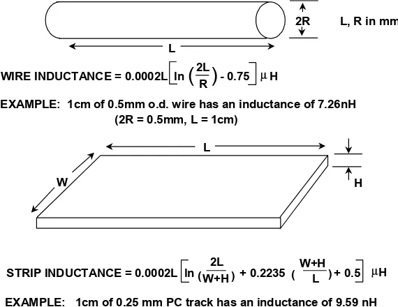
All conductors are inductive, and at high frequencies, the inductance of even quite short pieces of wire or printed circuit traces may be important. The inductance of a straight wire of length L mm and circular cross-section with radius R mm in free space is given by the first equation shown in Figure 9.9.
Figure 9.9: Wire and Strip Inductance Calculations
The inductance of a strip conductor (an approximation to a PC track) of width W mm and thickness H mm in free space is also given by the second equation in Figure 9.9.
In real systems, both these formulas turn out to be approximate, but they do give some idea of the order of magnitude of inductance involved. They tell us that 1 cm of 0.5-mm od wire has an inductance of 7.26 nH, and 1 cm of 0.25-mm PC track has an inductance of 9.59 nH—these figures are reasonably close to measured results.
At 10 MHz, an inductance of 7.26 nH has an impedance of 0.46 Ω, and so can give rise to 1% error in a 50-Ω system.
Mutual Inductance
Another consideration regarding inductance is the separation of outward and return currents. Kirchoff's Law tells us that current flows in closed paths—there is always an outward and return path. The whole path forms a single-turn inductor.
This principle is illustrated by the contrasting signal trace routing arrangements of Figure 9.10. If the area enclosed within the turn is relatively large, as in the upper "nonideal" picture, then the inductance (and hence the ac impedance) will also be large. On the other
L
2R L, R in mm
L
W H
EXAMPLE: 1cm of 0.5mm o.d. wire has an inductance of 7.26nH (2R = 0.5mm, L = 1cm)
2L
R µ
2L
L W+H
W+H
( )
)
WIRE INDUCTANCE = 0.0002L ln - 0.75 H
)
(
STRIP INDUCTANCE = 0.0002L ln + 0.2235 + 0.5( µH
[image:19.612.179.464.184.404.2]hand, if the outward and return paths are closer together, as in the lower "improved" picture, the inductance will be much smaller.
Figure 9.10: Nonideal and Improved Signal Trace Routing
Note that the nonideal signal routing case of Figure 9.10 has other drawbacks—the large area enclosed within the conductors produces extensive external magnetic fields, which may interact with other circuits, causing unwanted coupling. Similarly, the large area is more vulnerable to interaction with external magnetic fields, which can induce unwanted signals in the loop.
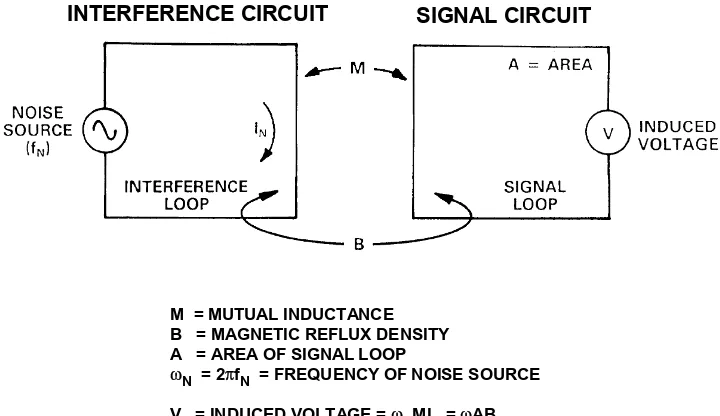
The basic principle is illustrated in Figure 9.11, and is a common mechanism for the transfer of unwanted signals (noise) between two circuits.
Figure 9.11: Basic Principles of Inductive Coupling LOAD
LOAD
LOAD
NONIDEAL SIGNAL TRACE ROUTING
IMPROVED TRACE ROUTING
LOAD
LOAD
LOAD
INTERFERENCE CIRCUIT SIGNAL CIRCUIT
M = MUTUAL INDUCTANCE B = MAGNETIC REFLUX DENSITY A = AREA OF SIGNAL LOOP
ωN = 2πfN = FREQUENCY OF NOISE SOURCE
As with most other noise sources, as soon as we define the working principle, we can see ways of reducing the effect. In this case, reducing any or all of the terms in the equations in Figure 9.11 reduces the coupling. Reducing the frequency or amplitude of the current causing the interference may be impracticable, but it is frequently possible to reduce the mutual inductance between the interfering and interfered with circuits by reducing loop areas on one or both sides and, possibly, increasing the distance between them.
[image:21.612.119.495.471.691.2]A layout solution is illustrated by Figure 9.12. Here two circuits, shown as Z1 and Z2, are minimized for coupling by keeping each of the loop areas as small as is practical.
Figure 9.12: Proper Signal Routing and Layout can Reduce Inductive Coupling
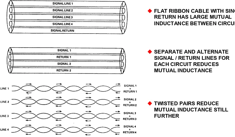
As also illustrated in Figure 9.13, mutual inductance can be a problem in signals transmitted on cables. Mutual inductance is high in ribbon cables, especially when a single return is common to several signal circuits (top). Separate, dedicated signal and return lines for each signal circuit reduces the problem (middle). Using a cable with twisted pairs for each signal circuit as in the bottom picture is even better.
Figure 9.13: Mutual Inductance and Coupling Within Signal Cabling
V1
V2
Z1
Z2
FLAT RIBBON CABLE WITH SINGLE RETURN HAS LARGE MUTUAL INDUCTANCE BETWEEN CIRCUITS
SEPARATE AND ALTERNATE SIGNAL / RETURN LINES FOR EACH CIRCUIT REDUCES MUTUAL INDUCTANCE
Shielding of magnetic fields to reduce mutual inductance is sometimes possible, but is by no means as easy as shielding an electric field with a Faraday shield (following section). HF magnetic fields are blocked by conductive material provided the skin depth in the conductor at the frequency to be screened is much less than the thickness of the conductor, and the screen has no holes (Faraday shields can tolerate small holes, magnetic screens cannot). LF and dc fields may be screened by a shield made of mu-metal sheet. Mu-mu-metal is an alloy having very high permeability, but it is expensive, its magnetic properties are damaged by mechanical stress, and it will saturate if exposed to too high fields. Its use, therefore, should be avoided where possible.
Ringing
An inductor in series or parallel with a capacitor forms a resonant, or "tuned", circuit, whose key feature is that it shows marked change in impedance over a small range of frequency. Just how sharp the effect is depends on the relative Q of the tuned circuit. The effect is widely used to define the frequency response of narrow-band circuitry, but can also be a potential problem source.
If stray inductance and capacitance (which may or may not be stray) in a circuit should form a tuned circuit, then that tuned circuit may be excited by signals in the circuit, and ring at its resonant frequency.
An example is shown in Figure 9.14, where the resonant circuit formed by an inductive power line and its decoupling capacitor may possibly be excited by fast pulse currents drawn by the powered IC.
Figure 9.14: Resonant Circuit Formed by Power Line Decoupling
While normal trace inductance and typical decoupling capacitances of 0.01-0.1µF will resonate well above a few MHz, an example 0.1-µF capacitor and 1 µH of inductance resonates at 500 kHz. Left unchecked, this could present a resonance problem, as shown in the left case. Should an undesired power line resonance be present, the effect may be minimized by lowering the Q of the inductance. This is most easily done by inserting a small resistance (~10 Ω) in the power line close to the IC, as shown in the right case.
SMALL SERIES RESISTANCE CLOSE TO IC REDUCES Q EQUIVALENT DECOUPLED POWER
LINE CIRCUIT RESONATES AT:
f = 1
2π√ LC
f = 1
2π√ LC
IC +VS
C1 L1
0.1µF 1µH
+VS
C1
L1
0.1µF
1µH R1
10Ω
Parasitic Effects in Inductors
Although inductance is one of the fundamental properties of an electronic circuit, inductors are far less common as components than are resistors and capacitors. As for precision components, they are even more rare. This is because they are harder to manufacture, less stable, and less physically robust than resistors and capacitors. It is relatively easy to manufacture stable precision inductors with inductances from nH to tens or hundreds of µH, but larger valued devices tend to be less stable, and large.
As we might expect in these circumstances, circuits are designed, where possible, to avoid the use of precision inductors. We find that stable precision inductors are rarely used in precision analog circuitry, except in tuned circuits for high frequency narrow band applications.
Of course, they are widely used in power filters, switching power supplies and other applications where lack of precision is unimportant (more on this in a following section). The important features of inductors used in such applications are their current carrying and saturation characteristics, and their Q. If an inductor consists of a coil of wire with an air core, its inductance will be essentially unaffected by the current it is carrying. On the other hand, if it is wound on a core of a magnetic material (magnetic alloy or ferrite), its inductance will be non-linear, since at high currents, the core will start to saturate. The effects of such saturation will reduce the efficiency of the circuitry employing the inductor and is liable to increase noise and harmonic generation.
As mentioned above, inductors and capacitors together form tuned circuits. Since all inductors will also have some stray capacity, all inductors will have a resonant frequency (which will normally be published on their data sheet), and should only be used as precision inductors at frequencies well below this.
Q or "Quality Factor"
The other characteristic of inductors is their Q (or "Quality Factor"), which is the ratio of the reactive impedance to the resistance, as indicated in Figure 9.15.
Figure 9.15: Inductor Q or Quality Factor
Q = 2πf L/R
The Q of an inductor or resonant circuit is a measure of the ratio of its reactance to its resistance.
The resistance is the HF and NOT the DC value.
It is rarely possible to calculate the Q of an inductor from its dc resistance, since skin effect (and core losses if the inductor has a magnetic core) ensure that the Q of an inductor at high frequencies is always lower than that predicted from dc values. Q is also a characteristic of tuned circuits (and of capacitors—but capacitors generally have such high Q values that it may be disregarded, in practice). The Q of a tuned circuit, which is generally very similar to the Q of its inductor (unless it is deliberately lowered by the use of an additional resistor), is a measure of its bandwidth around resonance. LC tuned circuits rarely have Q of much more than 100 (3-dB bandwidth of 1%), but ceramic resonators may have a Q of thousands, and quartz crystals tens of thousands.
Don't Overlook Anything
Remember, if your precision op amp or data-converter-based design does not meet specification, try not to overlook anything in your efforts to find the error sources. Analyze both active and passive components, trying to identify and challenge any assumptions or preconceived notions that may blind you to the facts. Take nothing for granted.
For example, when not tied down to prevent motion, cable conductors, moving within their surrounding dielectrics, can create significant static charge buildups that cause errors, especially when connected to high-impedance circuits. Rigid cables, or even costly low-noise Teflon-insulated cables, are expensive alternative solutions.
As more and more high-precision op amps become available, and system designs call for higher speed and increased accuracy, a thorough understanding of the error sources described in this section (as well those following) becomes more important.
REFERENCES:
9.1 PASSIVE COMPONENTS
1. James E. Buchanan, "Dielectric Absorption— It Can Be a Real Problem In Timing Circuits," EDN,
January 20, 1977, p 83.
2. Lew Counts and Scott Wurcer, "Instrumentation Amplifier Nears Input Noise Floor,"
Electronic Design, June 10, 1982.
3. W. Doeling, W. Mark, T. Tadewald, and P. Reichenbacher, "Getting Rid of Hook: The Hidden PC-Board Capacitance," Electronics, October 12, 1978, p 111-117.
4. Tarlton Fleming, "Data-Acquisition System (DAS) Design Considerations," WESCON '81 Professional Program Session Record No. 23.
5. Walter G. Jung and Richard Marsh, "Picking Capacitors, Parts I and II," Audio,February and March, 1980.
6. Robert A. Pease, "Understand Capacitor Soakage to Optimize Analog Systems", EDN, October 13, 1982, page 125.
7. Andy Rappaport, "Capacitors" EDN, October 13, 1982, page 105.
8. Specification MIL-PRF-19978G, Capacitors, Fixed, Plastic (or Paper-Plastic) Dielectric (Hermetically Sealed in Metal, Ceramic or Glass Cases), Established and Non-Established Reliability General Specification for, May 27, 1999.
9. Specification MIL-PRF-123B, Capacitors, Fixed, Ceramic Dielectric, (Temperature Stable and General Purpose), High Reliability, General Specification for, August 6, 1990.
10. Tantalum and Ceramic Surface Mount Capacitor Catalog, Kemet Electronics Corporation, P.O. Box 5928, Greenville, SC, 29606, 864-963-6300.
11. A general capacitor information resource: http://www.faradnet.com/
12. Southern and F-Dyne film capacitors, Southern Electronics, 215 Research Drive, Milford, CT, 06460, 203-876-7488.
13. Wesco film capacitors, Wesco Electrical Company, 201 Munson Street, Greenfield, MA, 01301, 413-774-4358.
14. Doug Grant and Scott Wurcer, "Avoiding Passive Component Pitfalls," The Best of Analog Dialogue, Analog Devices, 1991, p. 143-148.
15. RCD Components, Inc., 520 E. Industrial Park Drive, Manchester NH, 03109, 603-669-0054, http://www.rcd-comp.com
16. Steve Sockolov and James Wong, "High-Accuracy Analog Needs More Than Op Amps,"
Electronic Design, October 1, 1992, p.53.
17. Selection guide for digital potentiometers: http://www.analog.com/digitalpots
18. Precision Resistor Co., Inc., 10601 75th St. N., Largo, FL, 33777-1427, 727 541-5771, http://www.precisionresistor.com
20. Vishay/Dale Resistors, 2300 Riverside Blvd., Norfolk, NE, 68701-2242, 402 371-0800, http://www.vishay.com.
21. Beyschlag Resistor Products, PO Box 1220, D-25732 Heide, Germany, http://www.beyschlag.com
22. B. I. & B. Bleaney, Electricity & Magnetism, Oxford at the Clarendon Press, 1957, pp 23, 24, & 52. 23. Henry W. Ott, Noise Reduction Techniques in Electronic Systems, 2nd Edition, John Wiley, Inc.,
1988, ISBN: 0-471-85068-3.
24. G. W. A. Dummer, Materials for Conductive and Resistive Functions, Hayden, 1970.
Acknowledgements:
SECTION 9.2: PC BOARD DESIGN ISSUES
James Bryant, Walt Kester, Walt Jung
Printed circuit boards (PCBs) are by far the most common method of assembling modern electronic circuits. Comprised of a sandwich of insulating layer (or layers) and one or more copper conductor patterns, they can introduce various forms of errors into a circuit, particularly if the circuit is operating at either high precision or high speed. PCBs then, act as "unseen" components, wherever they are used in precision circuit designs. Since designers don’t always consider the PCB electrical characteristics as additional
components of their circuit, overall performance can easily end up worse than predicted. This general topic, manifested in many forms, is the focus of this section.
PCB effects that are harmful to precision circuit performance include leakage resistances; spurious voltage drops in trace foils, vias, and ground planes; the influence of stray capacitance, dielectric absorption (DA), and the related "hook." In addition, the tendency of PCBs to absorb atmospheric moisture, hygroscopicity, means that changes in humidity often cause the contributions of some parasitic effects to vary from day to day.
In general, PCB effects can be divided into two broad categories— those that most noticeably affect the static or dc operation of the circuit, and those that most noticeably affect dynamic or ac circuit operation.
Another very broad area of PCB design is the topic of grounding. Grounding is a problem area in itself for all analog designs, and it can be said that implementing a PCB based circuit doesn't change that fact. Fortunately, certain principles of quality grounding, namely the use of ground planes, are intrinsic to the PCB environment. This factor is one of the more significant advantages to PCB based analog designs, and an appreciable amount of this section is focused on this issue.
Some other aspects of grounding that must be managed include the control of spurious ground and signal return voltages that can degrade performance. These voltages can be due to external signal coupling, common currents, or simply excessive IR drops in ground conductors. Proper conductor routing and sizing, as well as differential signal handling and ground isolation techniques enables control of such parasitic voltages.
Resistance of Conductors
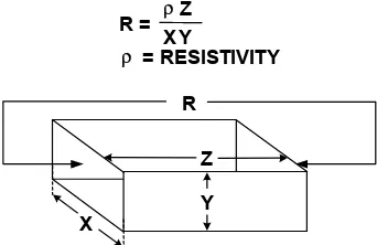
[image:28.612.198.369.228.339.2]Every engineer is familiar with resistors, although perhaps fewer are aware of their idiosyncrasies, as generally covered in Section 9.1. But far too few engineers consider that all the wires and PCB traces with which their systems and circuits are assembled are also resistors. In higher precision systems, even these trace resistances and simple wire interconnections can have degrading effects. Copper is not a superconductor—and too many engineers appear to think it is!
Figure 9.16 illustrates a method of calculating the sheet resistance R of a copper square, given the length Z, the width X, and the thickness Y.
Figure 9.16: Calculation of Sheet Resistance and Linear Resistance for Standard Copper PCB Conductors
At 25°C the resistivity of pure copper is 1.724×10⁻⁶Ωcm. The thickness of standard 1 ounce PCB copper foil is 0.036 mm (0.0014"). Using the relations shown, the resistance of such a standard copper element is therefore 0.48 mΩ /square. One can readily calculate the resistance of a linear trace, by effectively "stacking" a series of such squares end-end, to make up the line's length. The line length is Z and the width is X, so the line resistance R is simply a product of Z/X and the resistance of a single square, as noted in the figure.
For a given copper weight and trace width, a resistance/length calculation can be made. For example, the 0.25-mm (10-mil) wide traces frequently used in PCB designs equates to a resistance/length of about 19 mΩ/cm (48 mΩ /inch), which is quite large. Moreover, the temperature coefficient of resistance for copper is about 0.4% /°C around room temperature. This is a factor that shouldn't be ignored, in particular within low impedance precision circuits, where the TC can shift the net impedance over temperature.
R
X
Z Y ρ = RESISTIVITY R = ρ
X Z Y
SHEET RESISTANCE CALCULATION FOR 1 OZ. COPPER CONDUCTOR:
ρ = 1.724 X 10⁻⁶ Ωcm, Y = 0.0036cm R = 0.48 mΩ
= NUMBER OF SQUARES
R = SHEET RESISTANCE OF 1 SQUARE (Z=X) = 0.48mΩ/SQUARE
X
Z X
As shown in Figure 9.17, PCB trace resistance can be a serious error when conditions aren't favorable. Consider a 16-bit ADC with a 5-kΩ input resistance, driven through 5 cm of 0.25-mm wide 1-oz PCB track between it and its signal source. The track resistance of nearly 0.1 Ω forms a divider with the 5-kΩ load, creating an error. The resulting voltage drop is a gain error of 0.1/5000 (~0.0019%), well over 1 LSB (0.0015% for 16 bits).
Figure 9.17: Ohm’s Law Predicts >1 LSB of Error due to Drop In PCB Conductor
So, when dealing with precision circuits, the point is made that even simple design items such as PCB trace resistance cannot be dealt with casually. There are various solutions that can address this issue, such as wider traces (which may take up excessive space), the use of heavier copper (which may be too expensive), or simply choosing a high
impedance converter. But, the most important thing is to think it all through, avoiding any tendency to overlook items appearing innocuous on the surface.
Voltage Drop in Signal Leads—"Kelvin" Feedback
The gain error resulting from resistive voltage drop in PCB signal leads is important only with high precision and/or at high resolutions (the Figure 9.17 example), or where large signal currents flow. Where load impedance is constant and resistive, adjusting overall system gain can compensate for the error. In other circumstances, it may often be
removed by the use of "Kelvin" or "voltage sensing" feedback, as shown in Figure 9.18.
Figure 9.18: Use of a Sense Connection Moves Accuracy to the Load Point
16-BIT ADC, RIN = 5kΩ
SIGNAL SOURCE
0.25mm (10 mils) wide, 1 oz. copper PCB trace
5cm
Assume ground path resistance negligible
ADC with low RIN SIGNAL
SOURCE
Assume ground path resistance negligible FEEDBACK "SENSE" LEAD
HIGH RESISTANCE SIGNAL LEAD
In this modification to the case of Figure 9.17, a long resistive PCB trace is still used to drive the input of a high resolution ADC, with low input impedance. In this case
however, the voltage drop in the signal lead does not give rise to an error, as feedback is taken directly from the input pin of the ADC, and returned to the driving source. This scheme allows full accuracy to be achieved in the signal presented to the ADC, despite any voltage drop across the signal trace.
The use of separate force (F) and sense (S) connections at the load removes any errors resulting from voltage drops in the force lead, but, of course, may only be used in systems where there is negative feedback. It is also impossible to use such an
arrangement to drive two or more loads with equal accuracy, since feedback may only be taken from one point. Also, in this much-simplified system, errors in the common lead source/load path are ignored, the assumption being that ground path voltages are negligible. In many systems this may not necessarily be the case, and additional steps may be needed, as noted below.
Signal Return Currents
Kirchoff's Law tells us that at any point in a circuit the algebraic sum of the currents is zero. This tells us that all currents flow in circles and, particularly, that the return current must always be considered when analyzing a circuit, as is illustrated in Figure 9.19 (see References 7 and 8).
Figure 9.19: Kirchoff’s Law Helps in Analyzing VoltageDrops Around a Complete Source/Load Coupled Circuit
In dealing with grounding issues, common human tendencies provide some insight into how the correct thinking about the circuit can be helpful towards analysis. Most engineers readily consider the ground return current, "I", when they are considering a fully
differential circuit.
However, when considering the more usual circuit case, where a single-ended signal is referred to "ground", it is common to assume that all the points on the circuit diagram
I
I
GROUND RETURN CURRENT SIGNAL
SOURCE
RL
AT ANY POINT IN A CIRCUIT
THE ALGEBRAIC SUM OF THE CURRENTS IS ZERO OR
WHAT GOES OUT MUST COME BACK WHICH LEADS TO THE CONCLUSION THAT
ALL VOLTAGES ARE DIFFERENTIAL (EVEN IF THEY’RE GROUNDED)
II
G1 G2
where ground symbols are found are at the same potential. Unfortunately, this happy circumstance just ain't necessarily so!
This overly optimistic approach is illustrated in Figure 9.20, where, if it really should exist, "infinite ground conductivity" would lead to zero ground voltage difference
between source ground G1 and load ground G2. Unfortunately this approach isn’t a wise practice, and when dealing with high precision circuits, it can lead to disasters.
Figure 9.20: Unlike This Optimistic Diagram, it is Unrealistic to Assume Infinite Conductivity Between Source/Load Grounds in a Real-World System
A more realistic approach to ground conductor integrity includes analysis of the impedance(s) involved, and careful attention to minimizing spurious noise voltages. A more realistic model of a ground system is shown in Figure 9.21. The signal return current flows in the complex impedance existing between ground points G1 and G2 as shown, giving rise to a voltage drop ∆V in this path. But it is important to note that additional external currents, such as IEXT, may also flow in this same path. It is critical to understand that such currents may generate uncorrelated noise voltages between G1 and G2 (dependent upon the current magnitude and relative ground impedance).
Figure 9.21: A More Realistic Source-to-Load Grounding System View Includes Consideration of the Impedance Between G1-G2, Plus the Effect of Any
Non-Signal-Related Currents
SIGNAL
INFINITE GROUND CONDUCTIVITY
→
ZERO VOLTAGEDIFFERENTIAL BETWEEN G1 & G2 SIGNAL
SOURCE
ADC
G1 G2
SIGNAL
SIGNAL SOURCE
LOAD
∆V = VOLTAGE DIFFERENTIAL DUE TO SIGNAL CURRENT AND/OR EXTERNAL CURRENT FLOWING IN
GROUND IMPEDANCE
G1 G2
ISIG
IEXT
Some portion of these undesired voltages may end up being seen at the signal's load end, and they can have the potential to corrupt the signal being transmitted.
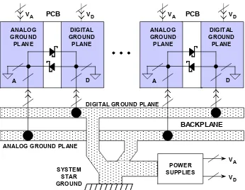
Grounding in Mixed Analog/Digital Systems
Walt Kester, James Bryant, Mike Byrne
Today's signal processing systems generally require mixed-signal devices such as analog-to-digital converters (ADCs) and digital-to-analog converters (DACs) as well as fast digital signal processors (DSPs). Requirements for processing analog signals having wide dynamic ranges increases the importance of high performance ADCs and DACs.
Maintaining wide dynamic range with low noise in hostile digital environments is dependent upon using good high-speed circuit design techniques including proper signal routing, decoupling, and grounding.
In the past, "high precision, low-speed" circuits have generally been viewed differently than so-called "high-speed" circuits. With respect to ADCs and DACs, the sampling (or update) frequency has generally been used as the distinguishing speed criteria. However, the following two examples show that in practice, most of today's signal processing ICs are really "high-speed," and must therefore be treated as such in order to maintain high performance. This is certainly true of DSPs, and also true of ADCs and DACs.
All sampling ADCs (ADCs with an internal sample-and-hold circuit) suitable for signal processing applications operate with relatively high speed clocks with fast rise and fall times (generally a few nanoseconds) and must be treated as high speed devices, even though throughput rates may appear low. For example, a medium-speed 12-bit successive approximation (SAR) ADC may operate on a 10-MHz internal clock, while the sampling rate is only 500 kSPS.
Sigma-delta (Σ-∆) ADCs also require high speed clocks because of their high oversampling ratios. Even high resolution, so-called "low frequency" Σ-∆ industrial measurement ADCs (having throughputs of 10 Hz to 7.5 kHz) operate on 5-MHz or higher clocks and offer resolution to 24-bits (for example, the Analog Devices AD77xx-series).
To further complicate the issue, mixed-signal ICs have both analog and digital ports, and because of this, much confusion has resulted with respect to proper grounding techniques. In addition, some mixed-signal ICs have relatively low digital currents, while others have high digital currents. In many cases, these two types must be treated differently with respect to optimum grounding.
Digital and analog design engineers tend to view mixed-signal devices from different perspectives, and the purpose of this section is to develop a general grounding philosophy that will work for most mixed signal devices, without having to know the specific details of their internal circuits.
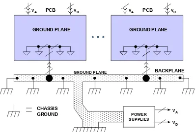
Ground and Power Planes
decoupling high frequency currents (caused by fast digital logic) but also minimizes EMI/RFI emissions. Because of the shielding action of the ground plane, the circuit's susceptibility to external EMI/RFI is also reduced.
Ground planes also allow the transmission of high speed digital or analog signals using transmission line techniques (microstrip or stripline) where controlled impedances are required.
The use of "buss wire" is totally unacceptable as a "ground" because of its impedance at the equivalent frequency of most logic transitions. For instance, #22 gauge wire has about 20 nH/inch inductance. A transient current having a slew rate of 10 mA/ns created by a logic signal would develop an unwanted voltage drop of 200 mV at this frequency flowing through 1 inch of this wire:
. mV 200 ns
mA 10 nH 20 t i L
v = × =
∆ ∆ =
∆ Eq. 9.1
For a signal having a 2-V peak-to-peak range, this translates into an error of about 200 mV, or 10% (approximate 3.5-bit accuracy). Even in all-digital circuits, this error would result in considerable degradation of logic noise margins.
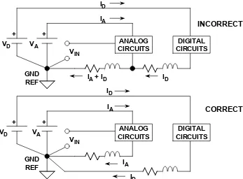
Figure 9.22 shows an illustration of a situation where the digital return current modulates the analog return current (top figure). The ground return wire inductance and resistance is shared between the analog and digital circuits, and this is what causes the interaction and resulting error. A possible solution is to make the digital return current path flow directly to the GND REF as shown in the bottom figure. This is the fundamental concept of a "star," or single-point ground system. Implementing the true single-point ground in a system which contains multiple high frequency return paths is difficult because the physical length of the individual return current wires will introduce parasitic resistance and inductance which can make obtaining a low impedance high frequency ground difficult. In practice, the current returns must consist of large area ground planes for low impedance to high frequency currents. Without a low-impedance ground plane, it is therefore almost impossible to avoid these shared impedances, especially at high frequencies.