Campus Universitario Dpto. de Teor´ıa de la Se˜nal y Comunicaciones Ctra. Madrid-Barcelona, Km. 36.6 28805 Alcal´a de Henares (Madrid) Telf: +34 91 885 66 90 Fax: +34 91 885 66 99
D. ROBERTO G ´OMEZ GARC´IA, Profesor Titular de Universidad del ´Area de Conocimiento de Teor´ıa de la Se˜nal y Comunicaciones de la Universidad de Alcal´a, y Da. DIMITRA PSYCHOGIOU, Investigador Cient´ıfico Senior de Universidad del
´
Area de Conocimento de Ingenier´ıa El´ectrica e Inform´atica de la Universidad de Purdue,
CERTIFICAN
Que la tesis “Advanced Microwave Filtering Devices Based on Signal-Interference Techniques”, presentada por D. Ra´ul Loeches S´anchez, realizada en el Departamento de Teor´ıa de la Se˜nal y Comunicaciones bajo nuestra direcci´on, re´une m´eritos suficientes para optar al grado de Doctor, por lo que puede procederse a su dep´osito y defensa.
Alcal´a de Henares, de de 2016.
Campus Universitario Dpto. de Teor´ıa de la Se˜nal y Comunicaciones Ctra. Madrid-Barcelona, Km. 36.6 28805 Alcal´a de Henares (Madrid) Telf: +34 91 885 66 90 Fax: +34 91 885 66 99
D. Ra´ul Loeches S´anchez ha realizado en el Departamento de Teor´ıa de la Se˜nal y Comunicaciones y bajo la direcci´on del Dr. D. Roberto G´omez Garc´ıa y del Dr. Da. Dimitra Psychogiou, la tesis doctoral titulada“Advanced Microwave Filtering Devices Based on Signal-Interference Techniques”, cumpli´endose todos los requisitos para la tramitaci´on que conduce a su posterior lectura.
Alcal´a de Henares, de de 2016.
EL COORDINADOR DEL PROGRAMA DE DOCTORADO
UNIVERSIDAD DE ALCAL ´
A
ADVANCED MICROWAVE FILTERING DEVICES BASED
ON SIGNAL-INTERFERENCE TECHNIQUES
PHD THESIS
Ra´
ul Loeches S´
anchez
PhD CandidateDEPARTAMENTO DE TEOR´IA DE LA SE ˜NAL Y COMUNICACIONES
Universidad de Alcal´a
ADVANCED MICROWAVE FILTERING DEVICES BASED
ON SIGNAL-INTERFERENCE TECHNIQUES
PHD THESIS
Author:
Ra´
ul Loeches S´
anchez
PhD Candidate
Advisors:
Roberto G´
omez Garc´ıa
Associate Professor with the Department of Signal Theory and Communications University of Alcal´a
Dimitra Psychogiou
Senior Research Scientist with the Department of Electrical and Computer Engineering
Purdue University
Tesis Doctoral
ADVANCED MICROWAVE FILTERING DEVICES BASED ON SIGNAL-INTERFERENCE TECHNIQUES
AUTOR: Ra´ul Loeches S´anchez DIRECTORES: Roberto G´omez Garc´ıa
Dimitra Psychogiou
El tribunal nombrado por el Mgfco. y Excmo. Sr. Rector de la Universidad de Alcal´a, el d´ıa de de 2016.
PRESIDENTE:
VOCALES:
SECRETARIO:
Realizado el acto de defensa y lectura de la Tesis el d´ıa de de 2016, en Alcal´a de Henares.
Calificaci´on:
EL PRESIDENTE LOS VOCALES
≪S´e breve en tus razonamientos,
que ninguno hay gustoso si es largo.≫
Institutional Acknowledgements
Among the projects and fellowships with different institutions that have given support to the developed research activities, it must be highlighted that:
• The research of this Ph.D. Thesis has been supported in part by the Commu-nity of Madrid and the University of Alcal´a, under the regional project “Ar-quitecturas Multi-Frecuencia de Banda Ultra-Ancha para Radares Coherentes de Alta Resoluci´on (AMBUARAD)”, reference CCG10-UAH/TIC-5983.
• The research of this Ph.D. Thesis has been supported in part by the University of Alcal´a, under the fellowship program “Ayudas de Iniciaci´on en la Actividad Investigadora”.
• The research of this Ph.D. Thesis has been supported in part by the Span-ish Ministry of Education, Culture and Sports, under the fellowship program “Formaci´on del Profesorado Universitario”, reference FPU13/01291.
• The research of this Ph.D. Thesis has been supported in part by the IEEE Mi-crowave Theory and Techniques Society, under the fellowship program “MTT-S Graduate Microwave Engineering Fellowship”.
Acknowledgements
I would like to express my sincere gratitude to my advisors Prof. Roberto G´omez Garc´ıa and Ph.D. Dimitra Psychogiou for their endless and invaluable guidance, patience and support during the realization of this Doctoral Thesis.
I would also like to thank Prof. Dimitrios Peroulis for hosting me in his research group at Purdue University.
I want to express special gratitude to my colleagues from the Signal Theory and Communications department, specially those from the ‘S22’ office.
Abstract
Radiofrequency-(RF)/microwave analog filters are essential components of tel-ecommunication and radar systems. Their basic function is to allow the transmission of some frequency components within a certain spectral range and inhibit, as much as possible, the other components that are out of this frequency interval. Required features for these devices are high selectivity, low in-band power insertion loss, low manufacturing cost, and small physical size. In compliance with these requirements, transversal signal-interference filters, mostly fabricated in planar technologies, have become an attractive alternative for moderate-to-ultra-wideband-(UWB) applica-tions. The term“signal interference” refers here to the philosophy adopted by these filter architectures in which the input signal is divided into multiple components that after passing through different electrical paths interfere at the output node. Thus, constructive signal-energy interactions in the passbands and destructive ones in the stopbands are produced for the shaping of the desired transfer function.
However, emerging applications, such as software-defined radio (SDR), continue to challenge the field of RF/microwave filters with even more stringent requirements to be met. New generations of wireless communication systems also demand high-frequency transceivers with multi-band and reconfigurable capabilities and, hence, need for flexible pre-selection filter solutions able to find a reasonable compromise among all their operational figures of merit.
The purpose of the present Ph.D. Dissertation is the analysis, design, construc-tion, and characterization of novel filtering topologies based on signal-interference principles that feature enhanced electrical performance, reduced occupied area, nar-row-to-wideband operation, and multi-function capability.
This Ph.D. Thesis can be divided into four different parts:
• In the first part, classic filtering techniques are combined with signal-interfer-ence principles to design novel filter architectures with advanced features in two senses: the attainment of low-order in-band group-delay profile for high-selectivity requirements through a new concept of “signal-interference source/ load coupling”, and the achievement of strongly-asymmetric transfer functions by means of stub-loading techniques.
fil-• The third part concentrates on extending the applicability of signal-interference filters to narrow-band designs. This is done through mixed-technology surface-acoustic-wave (SAW)/microstrip implementations.
• In the fourth part, multi-function microwave devices are developed under the signal-interference formalism. In particular, Wilkinson-type power di-viders, impedance transformers, and balanced frequency-selective devices with single/multi-band filtering capabilities are attained by embedding signal-inter-ference TFSs into them.
Resumen
Los filtros anal´ogicos de radiofrecuencia (RF) y microondas son componentes esenciales de los sistemas de telecomunicaci´on y radar. Su principal funci´on es permitir la transmisi´on de las componentes de frecuencia de un determinado rango espectral e inhibir, tanto como sea posible, aquellas componentes que se encuentran fuera de este intervalo de frecuencias. Dentro de las caracter´ısticas requeridas para este tipo de dispositivos se encuentran: alta selectividad, bajas p´erdidas de inserci´on en la banda de paso, bajos costes de fabricaci´on y peque˜no tama˜no f´ısico. En conformidad con estos requesitos, los filtros basados en t´ecnicas de interferencia transversal de se˜nales, principalmente fabricados en tecnolog´ıas planares, se han convertido en una alternativa atractiva para aplicaciones de banda moderada a ultra ancha. El t´ermino “interferencia transversal de se˜nales” se refiere a la filosof´ıa adoptada por este tipo de estructuras filtrantes, en las cuales la se˜nal de entrada se divide en m´ultiples componentes que despu´es de propagarse por distintos caminos el´ectricos interfieren en el puerto de salida.
Sin embargo, aplicaciones emergentes en el ´ambito de las telecomunicaciones tales como la radio definida por software (SDR), continuan desafiando el ´area de los filtros de RF y microondas con prestaciones cada vez m´as exigentes de satisfacer. Las nuevas generaciones de sistemas de comunicaci´on inal´ambrica tambi´en exigen un funcionamiento de tipo multi-banda y reconfigurable y, por lo tanto, necesitan de soluciones de filtrado flexibles capaces de encontrar un compromiso razonable entre todos sus par´ametros operacionales.
El prop´osito fundamental de la presente Tesis Doctoral es el an´alisis, dise˜no, con-strucci´on y caracterizaci´on de topolog´ıas filtrantes innovadoras basadas en principios de interferencia transversal de se˜nales de altas prestaciones con tama˜no reducido, funcionamiento de banda estrecha a moderada/ancha y capacidad multi-funcional.
Esta Tesis Doctoral se puede dividir en cuatro partes diferenciadas:
de redes transversales de elementos concentrados, el empleo de t´ecnicas de miniaturizaci´on mediante procedimientos de carga capacitiva y la propuesta de secciones filtrantes transversales de elementos concentrados basadas en el acoplador direccional de potencia en cuadratura.
• La tercera parte se centra en extender la aplicabilidad de los filtros basados en interferencia transversal de se˜nales a dise˜nos de banda estrecha. Esto se con-sigue a trav´es de realizaciones en tecnolog´ıa mixta de onda ac´ustica superficial y microstrip.
• En la cuarta parte, se desarrollan dispositivos de microondas multi-funcionales basados en principios de interferencia transversal de se˜nales. En particu-lar, se lleva a cabo el dise˜no de divisores de potencia Wilkinson, transfor-madores de impedancia y filtros balanceados con capacidad de filtrado de una o m´ultiples bandas de paso mediante la incorporaci´on de secciones de interfer-encia transversal.
List of Acronyms
3-D Three-Dimensional
3G 3rd Generation of mobile telecommunications
4G 4th Generation of mobile telecommunications
5G 5th Generation of mobile telecommunications
ACPS Asymmetric Coplanar Stripline
AW Acoustic Wave
BAW Bulk Acoustic Wave
BPF Bandpass Filter
BSF Bandstop Filter
BVD Butterworth-Van Dyke
CAD Computer-Aided Design
CRLH Composite Right/Left-Handed
dB Decibel
DC Direct Current
DGS Defected Ground Structure
DSPSL Double-Sided Parallel-StripLine
EM ElectroMagnetic
EMI ElectroMagnetic Interference
FEM Finite Element Method
FBW Fractional Bandwidth
GPS Global Positioning System
HTS High-Temperature Super-conductor
ICT Information and Communication Technologies
IEEE Institute of Electrical and Electronics Engineers
IL Insertion Loss
ITU International Communication Union
LPF Lowpass Filter
LTE Long Term Evolution
LTTC Low-Temperature Cofired Ceramic
MEMS MicroElectroMechanical Systems
MMIC Monolithic Microwave Integrated Circuit
MoM Method of Moments
NRN Non-Resonating Node
PCB Printed Circuit Board
PNA Power Network Analyzer
Q Quality factor
RF RadioFrequency
SAW Surface Acoustic Wave
SIR Stepped Impedance Resonator
SIW Substrate Integrated Waveguide
SDR Software-Defined Radio
SMA SubMiniature version A
SMD Surface Mount Device
SMT Surface-Mount Technology
SRF Self-Resonant Frequency
TFS Transversal Filtering Section
TRL Through-Reflect-Line
TZ Transmission Zero
UWB Ultra-WideBand
Contents
1 Introduction 1
1.1 Overview and motivation . . . 1
1.1.1 Brief description of the state-of-the-art . . . 2
1.1.2 Literature review on signal-interference filters . . . 5
1.2 Objective . . . 10
1.3 Thesis outline . . . 10
2 Design of mixed classic/signal-interference microwave filters 13
2.1 Filters with selectivity-enhancement based on signal-interference source-load coupling . . . 14
2.1.1 Theoretical foundations . . . 15
2.1.2 Experimental results . . . 17
2.2 Filters with frequency-asymmetrical response
based on the stub-loading technique . . . 28
2.2.1 Theoretical foundations . . . 29
2.2.2 Experimental results . . . 31
2.3 Conclusion . . . 35
3 Design of lumped-element-based signal-interference microwave
fil-ters 37
3.1 Filters based onLC T-type transversal circuit networks . . . 38
3.1.1 Theoretical foundations . . . 39
3.1.2 Simulation results . . . 41
3.2 Filters based on capacitive-loading and line-meandering techniques . 46
3.2.1 Theoretical foundations . . . 47
3.2.2 Experimental results . . . 51
3.3 Filters based on lumped-element quadrature-power-coupler-type TFSs 57
3.3.1 Concept . . . 60
4 Design of hybrid SAW/microstrip signal-interference microwave
fil-ters 69
4.1 Filters based on TFSs with embedded in-band one- and two-port SAW resonators as resonating nodes . . . 71
4.1.1 Concept . . . 72
4.1.2 Multi-TFS-cascaded designs . . . 75
4.1.3 Lumped-element designs . . . 78
4.1.4 Experimental results . . . 79
4.2 Filters based on TFSs with embedded one-port SAW resonator as non-resonating node . . . 82
4.2.1 Concept . . . 82
4.2.2 Multi-TFS-cascaded designs . . . 84
4.2.3 Comparison with the classic signal-interference TFS . . . 84
4.2.4 Experimental results . . . 88
4.3 Filters based on TFSs with embedded in-band SAW bandpass filter . 91
4.3.1 Concept . . . 91
4.3.2 Multi-TFS-cascaded designs . . . 94
4.3.3 Comparison with the classic signal-interference TFS . . . 96
4.3.4 Experimental results . . . 98
4.4 Conclusion . . . 104
5 Design of multi-function signal-interference microwave filtering
de-vices 107
5.1 Single- and multi-band Wilkinson-type filtering power dividers . . . 108
5.1.1 Theoretical foundations . . . 109
5.1.2 Experimental results . . . 118
5.1.3 Comparison with state-of-the-art multi-band Wilkinson-type power dividers . . . 131
5.2 Single- and multi-band filtering impedance transformers . . . 133
5.2.1 Theoretical foundations . . . 133
5.2.2 Experimental results . . . 136
5.3 Single- and dual-band balanced bandpass filters . . . 140
5.3.1 Theoretical foundations . . . 143
5.3.2 Experimental results . . . 147
5.4 Conclusion . . . 153
6.1 Concluding remarks . . . 155
6.2 Future research lines . . . 156
6.3 List of publications . . . 157
6.3.1 International journals . . . 158
6.3.2 International conferences . . . 158
6.3.3 Workshops . . . 159
List of Figures
1.1 Flow diagram of an N-channel feed-forward signal-interference microwave
filter. . . 3
1.2 Signal-interference TFS based on two in-parallel transmission-line segments. 4
1.3 Power transmission response of an ideal synthesized TFS based on two
transmission-line segments connected in parallel for Z1 = Z2 = 2Z0 and
m= 1. (n= 1: θ1(fd) = 90◦ and θ2(fd) = 450◦; n= 2: θ1(fd) = 90◦ and
θ2(fd) = 810◦ [10]). . . 4
2.1 Proposed filter concept (Z0 is the reference impedance, c is the coupling
factor, andθc andθ1 are the electrical lengths). . . 15
2.2 Ideal power transmission (|S21|) and reflection (|S11|) responses of a
synthe-sized enhanced-selectivity dual-band BPF and its basic dual-band TFS. . . 17
2.3 Layout and photograph of the manufactured microstrip BPF (prototype 1)
[51]. . . 19
2.4 Simulated and measured power transmission (|S21|), reflection (|S11|), and
group delay (τg) curves of the manufactured prototype 1, along with the simulated |S21| and τg curves of its basic low-order—third-order
hairpin-type—filter prototype [51]. . . 20
2.5 Influence of the NRN coupled-side length on the simulated power
transmis-sion response of the built prototype 1. . . 21
2.6 Layout and photograph of the manufactured microstrip BPF (prototype 2)
[51]. . . 22
2.7 Simulated and measured power transmission (|S21|), reflection (|S11|), and
group delay (τg) curves of the manufactured prototype 2, along with the simulated |S21| and τg curves of its basic low-order—third-order
hairpin-type—filter prototype [51]. . . 23
2.8 Layout and photograph of the manufactured microstrip LPF (pototype 3)
[51]. . . 24
2.9 Simulated and measured power transmission (|S21|), reflection (|S11|), and
group delay (τg) curves of the manufactured prototype 3, along with the simulated |S21| and τg curves of its basic low-order—stepped-impedance
2.11 Simulated and measured power transmission (|S21|) and reflection (|S11|)
parameters of the manufactured prototype 4, along with the simulated|S21|
and|S11|curves of its building basic—hybrid lumped/distributed-element—
filter prototype [124]. . . 27
2.12 Ideal power transmission (|S21|) and reflection (|S11|) responses of the
syn-thesized overall dual-band BPF and its building basic dual-band BPF [124]. 28
2.13 Layout of the devised stripline dual-band BPF (prototype 5) [124].
Non-redundant dimensions, in mm, are indicated. . . 28
2.14 Simulated (circuit and EM simulator) power transmission (|S21|) and
reflec-tion (|S11|) responses of the synthesized stripline dual-band BPF and power
transmission response of its microstrip counterpart [124]. . . 29
2.15 Schematic of the proposed stub-loaded bi-path TFS. . . 30
2.16 Ideal theoretical power transmission (|S21|) response of the synthesized
stub-loaded single-band bandpass TFS and its basic counterpart [10]. Design
parameters (M = 2, N = 3, Z0 = 50 Ω): Z1 = Z2 = Z
(1)
s1 = Z (3)
s1 =
Zs(1)2 = Zs(2)2 = 100 Ω, Zs(2)1 = 30 Ω,θ1(1)(fd) = 0.447π, θ
(2)
1 (fd) = 0.053π,
θ(1)2 (fd) = 0.947π, θ
(2)
2 (fd) = 3π/2, θ
(3)
2 (fd)=0.053π, θ
(1)
s1(fd)=θ
(3)
s1(fd)=π,
θ(2)s1(fd) =θ
(1)
s2(fd) =θ
(2)
s2(fd) =π/2. . . 31 2.17 Ideal theoretical power transmission (|S21|) response of the synthesized
stub-loaded dual-band bandpass TFS and its basic counterpart [10]. Design
pa-rameters (M = 3, N = 4, Z0 = 50 Ω): Z1 = 26.5 Ω, Z2 = 49.6 Ω,
Zs(1)1 = 97.6 Ω, Zs(3)1 =Zs(2)2 =Zs(3)2 = 20 Ω, Zs(4)1 = 100 Ω, Zs(1)2 = 57.6 Ω,
θ(1)1 (fd) = 0.541π, θ
(2)
1 (fd) = 0.053π, θ
(3)
1 (fd) = 0.418π, θ
(1)
2 (fd) = 0.429π,
θ(2)2 (fd) = 0.452π, θ
(3)
2 (fd) = 0.019π, θ
(4)
2 (fd) = 1.1π, θ
(1)
s1(fd) = 1.128π,
θ(2)s1(fd) =θ
(3)
s1(fd) =θ
(1)
s2(fd) =θ
(2)
s2(fd) =θ
(3)
s2(fd) =π/2,θ
(4)
s1(fd) = 1.034π. 32
2.18 Layout and photograph of the manufactured stub-loaded microstrip
dual-band BPF [54]. . . 33
2.19 Ideal theoretical, simulated, and measured power transmission (|S21|) and
reflection (|S11|) curves of the manufactured microstrip dual-band BPF
pro-totype [54]. . . 34
3.1 LC T-type equivalent model of a transmission-line segment. . . 39
3.2 Signal-interference TFS based on two in-parallel transmission-line segments.
(a) Basic approach. (b) Lumped-element model. . . 40
3.3 Ideal power transmission (|S21|) and reflection (|S11|) responses of a
syn-thesized example of a distributed-element TFS and two equivalent lumped-element realizations: convergence analysis [59].. . . 42
3.4 Layout of the final design of the lumped-element single-TFS LPF [59]. . . 43
3.5 Power transmission (|S21|) and reflection (|S11|) responses with the
attenu-ation mask of the designed LPF: ideal and real models [59]. . . 44
3.7 Power transmission (|S21|) and reflection (|S11|) responses with the
attenu-ation mask of the designed BPF: ideal and real models [59]. . . 45
3.8 Capacitive-loaded equivalent model of a quarter-wavelength
transmission-line segment. . . 47
3.9 Generalization of the equivalent model of Figure 3.8 toN capacitively-loaded transmission-line cells. . . 48
3.10 Classic signal-interference filter designs (θc = 90o) and their capacitively-loaded miniaturized equivalents with the approach of Figure 3.8 (casesθc = 75o, 60o, and 45o). . . 49
3.11 Schematic of the hybrid-ring-based TFS (Zr = 50 Ω,Z1 = 33.5 Ω, and Z2
= 45 Ω) [16]. . . 50
3.12 Schematic of the generalized-branch-line-coupler-based TFS (Zr1 = 30 Ω,
Zr2 = 95 Ω,Z1= 35 Ω, Z2 = 75 Ω,Zm = 49 Ω, andZs = 35.7 Ω [27]. . . 50
3.13 Classic signal-interference dual-band BPF filter design (θc = 90o) of Fig-ure 3.12 and their capacitively-loaded miniaturized equivalents withN = 1
(approach of Figure 3.8) and N = 2 (generalized approach of Figure 3.9). . 51
3.14 Photograph of the built miniaturized single-band BPF prototype and its
layout size comparison with its classic counterpart [72]. . . 52
3.15 Ideal, circuit-simulated, and measured power transmission (|S21|) and
reflec-tion (|S11|) curves of the devised miniaturized single-band BPF prototype
compared with those simulated for the classic design [72]. . . 54
3.16 In-band group-delay (τg) curves of the devised miniaturized single-band BPF
prototype compared with that simulated for the classic design [72]. . . 55
3.17 Photograph of the built miniaturized dual-band BPF prototype and its
lay-out size comparison with its classic counterpart [77]. . . 55
3.18 Ideal, circuit-simulated, and measured power transmission (|S21|) and
re-flection (|S11|) curves of the devised miniaturized dual-band BPF prototype
[77]. . . 56
3.19 Schematic of the switchable-bandwidth BPF composed by two inter-cascaded
Bagley-polygon-four-port-power-divider-based TFSs (Z1= 100 Ω,Z2= 100
Ω,Zs1A= 40 Ω,Zs2A= 60 Ω,Zs1B = 50 Ω,Zs2B = 100 Ω, andZcon= 20 Ω) [77]. . . 57
3.20 Layout size comparison of the miniaturized reconfigurable-bandwidth BPF
prototype with its classic counterpart [77]. . . 58
3.21 Ideal (dashed line) and EM-simulated (solid line) power transmission (|S21|)
and reflection (|S11|) curves of the devised miniaturized prototype 3
com-pared with those simulated for the classic design. State 1: stubs 1A, 2A, and 2B are ON, stub 1B is OFF. State 2: stub 1B is ON, stubs 1A, 2A, and
2B are OFF. State 3: all stubs are OFF. [77]. . . 59
3.22 TFSs based on quadrature power couplers. . . 61
3.23 Input/output matching and inter-stage cascading sections of the ideal
3.25 Input/output matching and inter-stage cascading sections of the ideal
syn-thesized dual-band BPF example [81]. . . 63
3.26 Power transmission (|S21|) and reflection (|S11|) responses of the ideal
syn-thesized dual-band BPF example and |S21| response of its building TFS
[81]. . . 64
3.27 Layouts of the designed UWB BPFs. (a) Prototype 1: lumped-element
realization. (b) Prototype 2: mixed distributed/lumped-element realization [81]. . . 66
3.28 Simulated power transmission (|S21|) and reflection (|S11|) curves of the
designed UWB BPF—Prototypes 1 and 2— [81]. . . 67
4.1 Detail and operating principle of the first type of hybrid-technology SAW/mi-crostrip TFS. . . 73
4.2 Examples of ideal synthesized power transmission (|S21|) response of the
TFS of Figure 4.1(a) and its embedded one-port SAW resonator: bandwidth control of the TFS as a function ofθ1(fd) andθ2(fd) (Z0= 50 Ω,Z1= 0.8Z0,
andZ2= 2Z0). . . 74
4.3 Schematic of the second type of hybrid-technology SAW/microstrip TFS
(building TFS, BVD model of the two-port SAW resonator, andN
-stage-series-cascaded BPF). . . 75
4.4 Power transmission (|S21|) and reflection (|S11|) curves for two examples of
the ideal synthesized TFS of Figure 4.3—transversal path 3 is ignored—and its embedded two-port SAW resonator. (a) Sharper rejection at the lower stopband (Z1 = 4Z0, Z2 = 4Z0, θ1(fd) = 42.6◦, and θ2(fd) = 182.4◦). (b) Sharper rejection at the upper stopband (Z1 = 4Z0, Z2 = 0.825Z0,
θ1(fd) = 50.8◦, andθ2(fd) = 178◦).. . . 76 4.5 Power transmission (|S21|) and reflection (|S11|) responses of an ideal
syn-thesized three-stage BPF shaped by the series-cascade connection of three
identical TFSs as in Figure 4.1. The power transmission parameters of
the one-port SAW resonator and the single TFS are also depicted. De-sign parameter values: Z1 = 2Z0, Z2 = 0.8Z0, Zc = 0.7Z0, θ1(fd) = 32◦,
θ2(fd) = 34◦, andθc(fd) = 19◦.. . . 77 4.6 Bandwidth control of the power transmission parameter (|S21|) of the
three-stage BPF by only acting onθ2(fd). . . 77 4.7 Power transmission (|S21|) and reflection (|S11|) responses of an ideal
synthe-sized two-stage BPF shaped by the series-cascade connection of two identical TFSs as in Figure 4.3—transversal path 3 is considered—. The power trans-mission parameters of the two-port SAW resonator and the single TFS are also depicted. Design parameter values: Z1 = 3.94Z0, Z2 = 4Z0, Z3 =Z0,
4.8 Power transmission (|S21|) and reflection (|S11|) responses of the three-stage
BPF design of Figure 4.1(a) and its lumped-element approximation. Design
parameter values—Z0= 50 Ω is assumed—for path 1: L1 = 10.52 nH and
C1= 1.94 pF; path 2: L2= 4.49 nH andC2= 5.13 pF; cascading network:
Lc = 2.15 nH and Cc= 3.41 pF. . . 79
4.9 Layout—non-redundant dimensions, in mm, are indicated—of the
three-stage SAW/microstrip BPF prototype based on the TFS of Figure 4.1(a) and photograph of the manufactured circuit for TRL-based characterization
of the one-port SAW resonator [98]. . . 80
4.10 Example of narrow-band BPF and one-port SAW-resonator responses. (a)
Power transmission (|S21|) and reflection (|S11|) parameters of the
three-stage BPF design—ideal transmission lines with one-port SAW-resonator BVD model, microstrip lines with commercial one-port SAW-resonator BVD model, and microstrip lines with commercial one-port SAW-resonator
meas-urements—. (b) Amplitude/phase transmission (S21) curves of the
assem-bled one-port SAW resonator and comparison with its BVD model [98]. . . 81
4.11 Detail and operating principle of the second type of hybrid-technology SAW/
microstrip TFS. . . 83
4.12 Examples of ideal synthesized power transmission (|S21|) and reflection (|S11|)
responses of the TFS of Figure 4.11(a) and its SAW device: bandwidth con-trol of the TFS as a function of θ1(fd) (Z1= 2Z0, Z2= 1.2Z0, Z3= 1.4Z0,
Z4= 1.2Z0,θ2(fd) = 70◦,θ3(fd) = 50◦, andθ4(fd) = 30◦). . . 85 4.13 Examples of ideal synthesized power transmission (|S21|) and reflection (|S11|)
responses of multi-TFS-series-cascaded BPFs—TFS of Figure 4.11(a)—and
its embedded SAW device and building TFS: identical TFSs (Z1 = 2Z0,
Z2 = 1.22Z0, Z3 = 1.4Z0, Z4 = 1.2Z0, θ1(fd) = 35◦, θ2(fd) = 70◦,
θ3(fd) = 50◦,θ4(fd) = 30◦, andθc(fd) = 85◦). . . 86 4.14 Ideal synthesized power transmission (|S21|) and reflection (|S11|) responses
of two-TFS-series-cascaded BPFs—TFS of Figure 4.11(a)—and its embed-ded SAW device and building TFS: dissimilar TFSs (TFS 1: Z1 = 2.1Z0,
Z2 = 1.14Z0, Z3 = 1.4Z0, Z4 = 1.1Z0, θ1(fd) = 35◦, θ2(fd) = 70◦,
θ3(fd) = 50◦, and θ4(fd) = 30◦; TFS 2: Z1 = 2.06Z0, Z2 = 1.2Z0,
Z3 = 1.4Z0, Z4 = 1.2Z0, θ1(fd) = 34◦, θ2(fd) = 70◦, θ3(fd) = 45◦, and
θ4(fd) = 35◦; inter-TFS cascading line: Zc = 1.6Z0, andθc(fd) = 65◦). . . 87 4.15 Comparison between the power transmission responses (|S21|) of the
three-stage BPF example of Figure 4.13 and its fully-planar classic counterpart of [12] for ideal transmission lines and microstrip lines of the planar substrate
Rogers RO4003C. . . 89
4.16 Layout and photograph of the manufactured two-stage SAW/microstrip
BPF prototype based on the TFS of Figure 4.11(a) [103]. . . 90
4.17 Ideal, simulated and measured power transmission (|S21|) and reflection
(|S11|) responses of the manufactured narrow-band BPF prototype based
on the TFS of Figure 4.11(a) along with the ideal and measured power
4.19 Examples of ideal synthesized power transmission (|S21|) and reflection (|S11|)
responses of the TFS of Figure 4.18(a) and its embedded narrow-band BPF: bandwidth control of the TFS as a function of impedance-line parameters (θ1(fd) = 181◦andθ2(fd) =θ3(fd) = 95◦). . . 95 4.20 Examples of ideal synthesized power transmission (|S21|) responses of the
TFS of Figure 4.18(a) and its embedded narrow-band BPF: TFS with strong
spectral asymmetry. . . 96
4.21 Examples of ideal synthesized power transmission (|S21|) and reflection (|S11|)
responses of multi-TFS-series-cascaded BPFs—TFS of Figure 4.18(a)—and its narrow-band BPF: identical TFSs (Z1 = 3.8Z0, Z2 = Z3 = 5.2Z0,
θ1(fd) = 181◦,θ2(fd) =θ3(fd) = 95◦, andθc(fd) = 0◦). . . 97 4.22 Comparison between the ideal power transmission (|S21|) and reflection
(|S11|) responses of a synthesized example of the TFS in Figure 4.18(a)—
narrower-band case of Figure 4.19—and its classic fully-planar counterpart in [12] for ideal transmission lines and microstrip lines implemented in the
substrate Rogers RO4003C. . . 98
4.23 Layout and photograph of the manufactured two-stage SAW/microstrip
BPF prototype 1 based on the TFS of Figure 4.18(a) [106]. . . 100
4.24 Simulated power transmission (|S21|) and reflection (|S21|) responses of the
manufactured two-stage SAW/ transmission-line BPF circuit prototype 1 based on the TFS of Figure 4.18(a) assuming ideal transmission-line sec-tions. The measured power transmission and reflection parameters of its
constitutive on-chip SAW BPF chip are also shown [106]. . . 101
4.25 EM simulated and measured power transmission (|S21|), reflection (|S11|),
and in-band group-delay (τg) responses of the manufactured two-stage SAW/ transmission-line BPF circuit prototype based on the TFS of Figure 4.18(a) [106]. . . 102
4.26 Layout and photograph of the manufactured three-stage SAW/microstrip
BPF prototype 2 based on the TFS of Figure 4.18(a) [103]. . . 103
4.27 Simulated power transmission (|S21|) and reflection (|S11|) responses of the
manufactured three-stage SAW/transmission-line BPF circuit prototype 2 based on the TFS of Figure 4.18(a) assuming ideal transmission-line sections and measured power transmission parameter of its constitutive on-chip SAW BPF chip [103].. . . 104
4.28 Simulated (EM) and measured power transmission (|S21|) and reflection
(|S21|) responses of the manufactured three-stage SAW/transmission-line
BPF circuit prototype 2 based on the TFS of Figure 4.18(a) [103]. . . 105
5.1 Detail of the single/multi-band Wilkinson-type filtering power divider and
5.2 S-parameters of an ideal synthesized single-band Wilkinson-type filtering power divider with asymmetrical power-division ratio between ports 3 and
2 of 4:1—k = 2—. Design values for Branch 1 (port 2): Z1 = Z0
√ 5/2,
Z2 =Z0
√
10, θ1(fd) = 90◦, and θ2(fd) = 270◦. Design values for Branch 2 (port 3): Z1 = (Z0/2)
√
5/8,Z2 =Z0
√
5/8, θ1(fd) = 90◦, and θ2(fd) = 270◦. R = 5Z0/2 and 90◦-at-fd electrical-length transformers at terminals 2 and 3 with impedances ofZ0
√
2 andZ0/
√
2, respectively, are included. . 111
5.3 S-parameters—amplitude and phase responses for S21 = S31—of an ideal
synthesized triple-band Wilkinson-type filtering power divider with
symmet-rical power-division ratio between ports 2 and 3—k = 1—. Design values
for both branches: Z1=Z0/
√
2,Z2=Z0
√
2,θ1(fd) = 270◦,θ2(fd) = 540◦, andR= 2Z0. . . 112
5.4 S-parameters—amplitude and phase responses for S21 = S31—of an ideal
synthesized sextuple-band Wilkinson-type filtering power divider with sym-metrical power-division ratio between ports 2 and 3—k= 1—. Design values for both branches: Z1=Z0/
√
2,Z2=Z0
√
2,θ1(fd) = 540◦,θ2(fd) = 720◦, andR= 2Z0. . . 113
5.5 Bandwidth control of the ideal synthesized triple-band Wilkinson-type filter-ing power splitter—power transmission and isolation responses—with
sym-metrical power division—k = 1—and according to the design equations
(5.1)-(5.5). . . 114
5.6 LC T-type equivalent model of a transmission line. . . 115
5.7 Power transmission (|S21|) and isolation (|S32|) responses of the ideal
syn-thesized triple-band Wilkinson-type filtering power divider and its lumped-element approximation (θ(fd) = 90◦,M = 2 and 6). . . 116
5.8 Schematic of two-stage 3-dB Wilkinson-type filtering power divider. . . 116
5.9 S-parameters in magnitude of the ideal synthesized two-stage bandpass
3-dB Wilkinson-type filtering power divider. Design values for TFS A:Z1A= 1.122Z0, Z2A = 2.026Z0, θ1A(fd) = 90◦, and θ2A(fd) = 270◦. Design values for TFS B: Z1B = 0.486Z0, Z2B = 0.846Z0, θ1B(fd) = 90◦, and
θ2B(fd) = 270◦. Cascading line:Zm= 2.236Z0andθm(fd) = 90◦. Resistor:
R= 2Z0. . . 117
5.10 Schematic of stepped-impedance-line signal-interference TFS. . . 117
5.11 S-parameters in magnitude of the ideal synthesized spectrally-asymmetrical
dual-band 3-dB Wilkinson-type filtering power divider. Design
parame-ter values for the stepped-impedance-line TFS: Za = (3
√
2/5)Z0, Zb = 11Z0/(5
√
2), Z2=Z0
√
2,θa(fd) = 69.12◦,θb(fd) = 35◦, andθ2(fd) = 180◦. Resistor: R= 2Z0. . . 118
5.12 Layout and photograph of the manufactured triple-band Wilkinson-type
fil-tering power divider (prototype 1) [124]. . . 120
5.13 Ideal theoretical, EM-simulated, and measured S-parameters in magnitude
5.15 Ideal theoretical, EM-simulated, and measuredS-parameters in magnitude of the manufactured microstrip quad-band Wilkinson-type filtering power divider prototype [125].. . . 124
5.16 Layout and photograph of the manufactured lumped-element dual-band
Wilkinson-type filtering power divider (prototype 3) [125]. . . 126
5.17 Ideal theoretical, EM-simulated, and measuredS-parameters in magnitude
of the manufactured lumped-element dual-band Wilkinson-type filtering power divider prototype [125].. . . 127
5.18 Two-branch channelized active BPF. . . 129
5.19 Ideal power transmission (|S21|) response of the ideal synthesized
channel-ized BPF based on the new and classic—n = 2 and 3—approaches along
with the ideal transfer function of its low-order passive BPF. . . 129
5.20 Layout of the single-band filter/power-dividing stage and photograph of the
manufactured two-branch channelized active BPF (prototype 4) [125].. . . 130
5.21 Measured power transmission (|S21|), reflection (|S11|), and reverse-isolation
(|S12|) curves of the manufactured channelized BPF prototype along with
the measured power transmission response of its low-order coupled-line-type filter [125]. . . 131
5.22 Signal-interference TFS for generalized input/output impedances. . . 134
5.23 Power transmission (|S21|) and reflection (|S11|) responses of the ideal
syn-thesized triple-band signal-interference TFSs forRin=Z0 andRL= 2Z0. . 135
5.24 Multi-stage filtering impedance transformer with signal-interference TFSs . 135
5.25 Power transmission (|S21|) and reflection (|S11|) responses—for Rin = 50
Ω and RL = 25 Ω—and prefixed input-power-matching mask of the ideal
synthesized dual-band filtering impedance transformer [130].. . . 137
5.26 Layout and photograph of the manufactured microstrip dual-band filtering
impedance transformer (prototype 1) [130]. . . 138
5.27 Simulated—circuit-model and EM— and measured power reflection responses
(|S11|) and simulated—circuit-model—power transmission response (|S21|)
of the manufactured microstrip dual-band filtering impedance transformer
(prototype 1)—Rin= 50 Ω andRL= 25 Ω—, [130]. . . 139
5.28 Power transmission (|S21|) and reflection (|S11|) response—for Rin = 50
Ω and RL = 25 Ω—and prefixed input-power-matching mask of the ideal
synthesized UWB single-band filtering impedance transformer [130].. . . . 140
5.29 Layout and photograph of the manufactured microstrip UWB single-band
filtering impedance transformer (prototype 2) [130]. . . 141
5.30 Simulated—circuit-model and EM— and measured reflection responses (|S11|)
and simulated—circuit-model—power transmission response (|S21|) of the
manufactured microstrip UWB single-band filtering impedance transformer
5.31 Balanced filter: differential two-port or single-ended four-port network. . . 143
5.32 Engineered balanced BPF with embedded signal-interference TFS (the
val-ues of the electrical lengths are calculated at the design frequency fd). . . 144 5.33 Ideal power transmission (|S21|) and reflection (|S11|) responses of the
dif-ferential and common modes of a synthesized example of the balanced BPF circuit in Figure 5.32 and|S21|and|S11|coefficients of its embedded
signal-interference TFS. . . 145
5.34 Two-TFS series-cascaded balanced BPF with embedded signal-interference
TFS. . . 146
5.35 Ideal power transmission (|S21|) and reflection (|S11|) responses of an
exam-ple two-TFS single-band balanced BPF in differential and common modes and|S21|coefficients of its building signal-interference TFSs. . . 148
5.36 Ideal power transmission (|S21|) and reflection (|S11|) responses of example
of synthesized two-TFS balanced dual-band BPF in differential and common modes and|S21| coefficients of its building signal-interference TFSs. . . 149
5.37 Layout and photograph of the manufactured microstrip balanced single-band
BPF prototype [150]. . . 151
5.38 Ideal, simulated (circuit and EM model), and measured power
transmis-sion (|S21|) and reflection (|S11|) responses of the manufactured microstrip
balanced single-band BPF prototype [150]. . . 152
5.39 Ideal, simulated (circuit and EM model) and measured group-delay (τdd
g ) responses of the manufactured microstrip balanced single-band BPF proto-type in differential mode [150]. . . 153
5.40 Simulated and measured common-to-differential-mode (|Scd
21|) and
differential-to-common-mode (|S21dc|) power transmission responses of the manufactured
List of Tables
3.1 Lumped-element components of the single-TFS LPF in Figure 3.4 based on
LC T-type networks. . . 43
3.2 Lumped-element components of the BPF in Figure 3.6 based onLCT-type
networks. . . 45
3.3 Lumped-element components of the ideal synthesized UWB BPF example. 62
3.4 Lumped-element components of the ideal synthesized dual-band BPF example. 64
3.5 Lumped-element components of the designed UWB BPF. . . 65
5.1 Components for the manufactured lumped-element dual-band filter/divider
prototype. . . 125
5.2 Comparison of multi-band Wilkinson-type power dividers based on
Chapter 1
Introduction
1.1
Overview and motivation
Since the advent of information and communication technologies (ICT), the so-ciety has witnessed a technological race where ever more sophisticated services are offered to the end user. Clear evidence of this technological evolution is the current and the upcoming generation of mobile telecommunications—4th generation of mo-bile telecommunications (4G) and 5thgeneration of mobile telecommunications (5G), respectively—capable of providing with voice telephony, video calls, mobile web ac-cess, high-definition mobile TV, video on demand, and cloud computing among other services, all of them demanding a large amount of bandwidth [1]–[3]. If, in addition to the cellular communication network, other signals from services such as TV and radio broadcasting, global positioning system (GPS), and remote sensing and radar for both civilian and defense applications are radiated to the free space, the final result is the current saturation of the RF spectrum. For the coexistence of the aforementioned services, a more efficient use of the electromagnetic (EM) spectrum is therefore required. This is reflected in the evolution of RF/microwave architectures and the high-frequency devices integrating them, in which enhanced electrical performance, flexibility, and size compactness are basic requested features.
wire-less technology—also known as Worldwide Interoperability for Microwave Access (WiMAX)—at 3500 MHz (all these frequencies according to Spanish legislation [6]).
It is in this context that significant effort has been made to meet these stringent specifications for RF/microwave filters, following two main trends: the invention of new materials and fabrication processes and the development of innovative and more efficient filtering topologies. However, despite the enormous amount of research effort in this area, there are still design limitations for these devices to be overcome.
1.1.1 Brief description of the state-of-the-art
Well-known RF/microwave filter design procedures start with the synthesis of a lumped-element equivalent low-pass prototype, following a Butterworth or Cheby-shev approach, which is subsequently transformed into the required high-frequency filter. This ideal lumped-element circuit is then turned into a physically imple-mentable structure that often consists of electromagnetically-coupled resonators [7]. This procedure has been widely extended in RF/microwave filter design due in large part to its systematic methodology. However, the selectivity in this type of filters for basic responses is rather limited and, consequently, cross-coupling between non-adjacent resonators is needed in case of high-selectivity requirements. These new couplings generate TZs at both sides of the passband range at the expense of in-creased design complexity and higher in-band group-delay variation when the TZs are placed close to the passband [8]. Other shortcomings of basic coupled-resonator-based approaches to be remarked are their difficulty to feature wideband filtering actions, due to physical constraints imposed by the minimum separation between coupled lines feasible in the fabrication process, and the limitation of the maximum number of experimentally-proven passbands in multi-band designs to date.
1.1 Overview and motivation
are needed for their development.
The other alternative for the realization of advanced microwave filters is the proposal of novel circuit topologies. To this end, a variety of untypical configura-tions have been recently reported, among which signal-interference filters are a good exponent. Inspired by classic digital filter design techniques, their operating prin-ciple is to split the signal to be processed into several weaker components which, after traveling by different electrical paths, interfere at the output port. For illus-tration purposes, Figure 1.1 depicts the flow diagram of an N-channel feed-forward structure in which most of transversal signal-interference filters are based on. Note that this transversal-like approach permits each signal component to be individually processed by the correspondent branch. Subsequently, a large variety of filtering re-sponses can be synthesized by properly combining those particular channel actions at the overall output node [9].
Input Output
S (f)21 C0
S (f)21 C1
S21 (f)
C(N-1) Channel 0
Channel 1
ChannelN-1
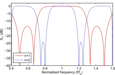
Figure 1.1: Flow diagram of anN-channel feed-forward signal-interference microwave filter. As an example of this filtering philosophy, the most basic signal-interference TFS is introduced here. As can be seen in Figure 1.2, it consists of two different transmission-line segments connected in parallel. This configuration was first intro-duced in 2005 for the design of high-selectivity wideband bandpass filters (BPFs) with high power rejection levels in the stopbands [10]. The design parameters are then determined by enforcing the power transmission maximum condition at the cen-ter frequency,f0. By properly adjusting the electrical lengths and the characteristic impedances of both transmission-line segments according to the design equations and guidelines provided in [10], the locations of the TZs closest to the passband and the 3-dB relative bandwidth can be controlled. This is illustrated in Figure 1.3 in which, for a given pair of line impedances Z1 and Z2 and an index m, different values of the index n vary the passband-width. Moreover, it is worth mentioning that higher-order filters can be attained when multiple TFSs are cascaded in series. This leads to a subsequent increase in the attenuation levels in the stopbands and the sharpness of the cut-off slopes.
Input
Z ,
Output
1
θ
1Z ,
2θ
2Figure 1.2: Signal-interference TFS based on two in-parallel transmission-line segments.
0.4 0.6 0.8 1 1.2 1.4 1.6
−40 −35 −30 −25 −20 −15 −10 −5 0
Normalized frequency (f/f d)
S21
(dB)
n=1 n=2
Figure 1.3: Power transmission response of an ideal synthesized TFS based on two transmission-line segments connected in parallel forZ1 =Z2 = 2Z0 and m = 1. (n = 1:
1.1 Overview and motivation
BPF, presented a remarkable contribution to the field of multi-band BPFs since only quad-band filtering responses had been achieved to that moment. Furthermore, this circuit topology was generalized for any arbitrary number of passbands unlike prior-art quad-band BPF alternatives based on complex multi-layer and defected-ground structures (DGSs) [13], [14]. Thus, by means of such a simple circuit network, several of the general requirements in microwave filters were accomplished: high selectivity for moderate-to-wideband passbands, stopbands with high power rejection levels, low in-band power insertion loss due to the avoidance of EM couplings, and multi-band operation with inter-multi-band transmission nulls.
In addition to this contribution, numerous topologies based on these signal-interference principles have been proposed over the last decade. The most noticeable ones, along with their advantages, will be reviewed in Section 1.1.2.
1.1.2 Literature review on signal-interference filters
The framework of this Ph.D. Dissertation is defined within the field of microwave signal-interference filter design. Thus, this sub-section is intended to provide a short report of main works published to date concerning this RF filtering philosophy. Notwithstanding, a thorough review of the available literature is included in every chapter of this Thesis regarding the subject of interest.
practical demonstrator.
The realizations reported in the preceding paragraph concentrate on the synthesis of single-band BPFs. However, signal-interference principles have been also applied to the synthesis of other classes of transfer functions. Thus, the work presented in [21] was aimed at the design of a sharp-rejection lowpass filter (LPF) with ultra-large stopband. Its principle consists of cascading several dissimilar TFSs with adjacent stopbands so as to broaden the overall attenuated band. Its main advantage when compared to other LPF solutions available in the open literature is the avoidance of coupled-line stages and patterned ground-planes. It simplifies the circuit simulation and manufacturing processes. For illustrative purposes, three LPF prototypes with 1-GHz cut-off frequency were built in [21]. The first one, in which the TFSs are based on uniform-based hybrid rings, exhibits a minimum stopband power rejection level of 20 dB over a frequency range of 4.6 GHz. In the second approach, the minimum out-of-band attenuation level is increased up to 40 dB over a frequency range of 4.2 GHz by allowing heterogeneous line-impedance segments in the TFSs. Finally, the third approach replaces the hybrid ring configuration forming the TFSs with branch-line hybrids. It shows a minimum attenuation level in the stopband of 30 dB over 3.3 GHz. In addition, a modified version of the latter was utilized to realize a BPF prototype exhibiting a 3-dB relative bandwidth of 110% around 640 MHz while keeping the same broad upper attenuated band.
From the point of view of bandstop-type implementations, there have been many recent contributions as well. By simply modifying the electrical lengths and line impedances of the well-known bi-path signal-interference TFS of Figure 1.2, sharp-rejection wideband bandstop filters (BSFs) can be designed, as in [22]. Particularly, two one-stage BSF prototypes were implemented in [22] showing a relative band-width of 30% around 1 GHz for minimum 20-dB and 30-dB stopband attenuation levels, respectively. For the same purpose, a structure based on an open-ended coupled-line coupler in parallel with a transmission-line segment was used in the design of a BSF with a minimum 20-dB rejection bandwidth of 100% centered at 2 GHz in [23]. Following this trend, a novel circuit topology which includes open-loop resonators in the signal-propagation path with larger electrical length of the bi-path TFS was devised in [24]. It allows to add two additional TZs with respect to its two in-parallel-transmission-line-type counterpart. This BSF topology was experimentally proven by an implemented prototype with a 20-dB-referred rejection relative bandwidth of 41% around 2 GHz. The last example of signal-interference BSF described in [25] consists of a single TFS in which aU-shaped short-circuited stepped-impedance resonator (SIR) structure is embedded again in the electrically-longer path of the conventional approach. By doing so, an attenuation band with four transmission nulls and sharp cut-off slopes was achieved. Its implemented pro-totype showed a minimum 20-dB rejection bandwidth of 50% centered at 2.4 GHz.
prin-1.1 Overview and motivation
ciple is to add open-circuited stubs at the input and output terminals of the entire structure. As practical example, a two-stage 1.5/2.5 GHz fourth-order dual-band BPF prototype with 3-dB absolute bandwidth of 690 MHz in both passbands was built and tested. Another contribution is found in [27], where the generalized branch-line hybrid is used to perform a 2.1/3.9 dual-band wideband filtering with an abso-lute bandwidth of 450 MHz for both transmission bands by cascading in series two TFSs. In [28], the adopted strategy focused on the employment of a stub-loaded Bagley-polygon four-port power divider as a TFS. In this manner, two passbands fairly close to each other at 2.75 and 3.25 GHz—3-dB absolute bandwidth of 125 MHz for both—were obtained in a two-stage realization. Moreover, Bagley-polygon-type-based structures were utilized to develop quad-band bandpass and dual-band bandstop transfer functions by properly modifying the length of the stubs according to the design equations in [20]. Lastly, other innovative approaches are the ones reported in [29], where hybrid couplers arranged in reflection mode are loaded by double stubs in the input and isolated ports. The short-ended loading stubs trans-form the inherent bandstop response of the TFSs into two-pole dual-band wideband bandpass transfer functions, while the open-ended stubs increase the power rejection levels in the attenuated band between both passbands. The first reported prototype with the passbands centered at 0.63 and 2.37 GHz and absolute bandwidth of 435 MHz is based on the hybrid-ring-based TFS. The second circuit with the passbands around 0.68 and 2.32 GHz and 3-dB absolute bandwidth of 675 MHz exploits the branch-line-hybrid-based TFS. Both prototypes consist of the series-cascade connec-tion of two TFSs.
The topologies reviewed at this point demonstrate the capability of signal-inter-ference principles to synthesize a large variety of filtering transfer functions, going from bandpass to bandstop ones and from single- to multi-band ones. However, they all exhibit frequency-symmetrical responses with regard to the design frequency fd. Note that spectral asymmetry can be particularly interesting in multi-channel/multi-mode communication systems asssociated to different services. For instance, in du-plexing devices, the inter-channel power-rejection levels inherent to each channel filter can be increased at one stopband side by means of asymmetrical patterns in the frequency response. Other scenario is in multi-standard systems where these passbands might need of distinct absolute bandwidth. This has been partially ad-dressed so far in signal-interference approaches by replacing the uniform-impedance lines that shape these TFSs with stepped-impedance lines. Following the theoretical foundations in [30], a duplexer with the lower and upper channels centered at 1.7 and 2.25 GHz and of absolute bandwidths of 395 and 265 MHz, respectively, were built. Specifically, an inter-channel rejection level higher than 40 dB is attained at both output terminals. In the same work, a two-stage 1.3/2.5 GHz dual-band BPF with 3-dB absolute bandwidths of 400 and 100 MHz, respectively, was also reported.
are expounded hereafter. In transversal approaches, the sub-components of the sig-nal, after being divided at the input node, are individually amplitude-weighted and time-delayed before they are combined at the output node. Recursive approaches include feedback loops from the output to the input terminal. This allows to reduce the number of weighting elements needed for a given degree of filtering selectivity but compromises circuit stability [31]. Channelized filters, as in [9], [32], and [33], can be viewed as generalized transversal filters based on frequency-selective ampli-tude weighting. This results in a reduction in the number of feedforward branches. As an extension of these works, recursive active filtering structures can be modified to feature dual-band operation, as demonstrated in [34]. To this aim, the conven-tional transmission line section in the feedback branch is replaced with a composite right/left-handed (CRLH) transmission-line segment, that meets the phase condi-tion needed for the recursive-filter operacondi-tion in two arbitrary frequencies—788 and 1700 MHz in the built prototype—. As a last example of signal-interference-based active filters, [35] introduced a novel two-stage recursive BPF in silicon technology, in which center frequency—around 2 GHz in this case—, bandwidth, and power transmission gain can be independently tuned. This work also presented a MMIC reconfigurable three-branch channelized BPF based on a new divider arrangement.
1.1 Overview and motivation
BPF based on two cascaded TFSs formed by the generalized Bagley-polygon-type four-port power divider. It results in four states with 3-dB relative bandwidth of 16%, 29%, 34% and 48%—these two prototypes are synthesized at fd=2 GHz—.
Despite the large variety of signal-interference filters developed up to now, as evidenced by the previous review, there are still some shortcomings to overcome. To sum up, some of the main remaining limitations for this class of filtering configura-tions are as follows:
• The combination of classic filtering techniques with signal-interference ones can be even further exploited in order to carry out more efficient filtering actions. Among the unsolved problems on signal-interference filters with sharp-rejection capabilities, a common lack is the noticeable in-band group-delay variation. This means that the more selective the filter is, then the larger the in-band group-delay variation is. This factor is particularly important on digital communications, sometimes causing an undesired effect known as inter-symbol interference (ISI) [40]. Concerning multi-band communication systems, another design aspect to be addressed is the incorporation of spectral asymmetry in their transfer functions. This is difficult to achieve due to the fact that the lengths of transmission-line segments forming signal-interference filters are conventionally set as integer multiples of 90 degrees, leading to spectral symmetry and periodic frequency responses with regard to the design frequency,fd, in the interval [0,2fd].
• Most of the experimentally-proven signal-interference filters have been devel-oped in fully-planar technologies. This gives rise to large physical circuit size, especially for designs aimed at the lower part of the RF spectrum, where a hybrid or pure-lumped-element implementation would be more appropriate.
• The practical suitability of signal-interference techniques to design very-narrow-band BPFs remains still unexplored. In such case, the conventional topologies proposed so far would need excessive lengths for the transmission-line paths of their TFSs, resulting in an unviable implementation owing to the conse-quent huge circuit size and the insertion-loss limitations caused by the planar substrate.
• The design of multi-function microwave devices is a current hot topic that needs to be explored under the signal-interference formalism. This means the combination of multiple RF processing functions, such as filtering, power splitting, power combination, impedance transformation or amplifying, among others, in the same electrical network. These multi-function components have benefits in terms of size and optimized electrical performance.
1.2
Objective
Once the motivation and the state-of-the-art related to the topic of microwave signal-interference filters have been summed up, the aim of the current Ph.D. Thesis can be established. This is as follows:
“Analysis, design, construction and characterization of novel advanced microwave filtering devices based on transversal signal-interference tech-niques”
This general purpose has been divided into four main sub-objectives, as indicated below:
1. Proposal of novel microwave filtering circuits exploiting the combi-nation of classic filtering techniques and signal-interference princi-ples; specifically, the improvement of the filtering selectivity without sacri-ficing the in-band group-delay response and the achievement of asymmetric frequency responses on signal-interference filters for different kinds of filtering functions, ranging from low-pass to multi-band type, will be approached.
2. Invention of hybrid- and lumped-element-based feedforward signal-interference filtering networks; here, especial emphasis will be made on the proposal of size-reduced circuit models suitable to be implemented in the lower part of the microwave band.
3. Development of very-narrow-band transversal signal-interference fil-tering sections;in particular, the implementation of signal-interference BPFs in hybrid transmission-line/SAW-resonator technology will be contemplated.
4. Design of multi-function microwave circuits inspired on transver-sal signal-interference techniques;this research task will mainly focus on dual-function passive components with single/multi-band operation and their application to more-complex high-frequency components.
Throughout the chapters of this Ph.D. Thesis, a considerable effort will be made in obtaining theoretical design methodologies for the suggested signal-interference microwave circuits. In addition, several proof-of-concept prototypes will be imple-mented to experimentally validate the described topologies.
1.3
Thesis outline
In this section, the detailed thesis plan is expounded. The structure is divided into five more chapters, apart from this introductory one, according to the research tasks previously described.
1.3 Thesis outline
between the input and the output nodes of the original basic filter to create two signal-propagation paths. This technique is verified by means of the physical re-alization of low-pass, high-pass, and single/multi-band bandpass filtering circuits. On the other hand, a principle based on the inclusion of loading stubs in specific locations of conventional signal-interference TFSs is devised with the aim of obtain-ing frequency-asymmetrical filterobtain-ing responses. A dual-band BPF prototype is built and measured to corroborate its practical usefulness.
In Chapter 3, three different topologies for the design of compact lumped-element and hybrid distributed/lumped-lumped-element circuits are presented, in order to reduce the circuit size of signal-interference filters in the lower part of the RF spec-trum. The idea behind the first approach is to replace short-length transmission-line segments withLCT-type transversal circuit networks. As a proof of concept, a LPF and a BPF are designed at the layout level. In the second methodology, the minia-turization of signal-interference filters is faced up by means of capacitive-loading and line-meandering techniques. For the verification of the proposed approach, single-and multi-bsingle-and BPF prototypes are implemented. In both previous synthesis tech-niques, the trade-off between frequency-response convergence and level of size reduc-tion with regard to the convenreduc-tional counterpart is carefully examined. Finally, in the third approach, the TFS based on the distributed-element quadrature coupler ar-ranged in reflection mode is substituted by a pure-lumped-element counterpart. Its suitability is demonstrated through lumped- and mixed distributed/lumped-element realizations at the simulation level. The insertion loss and the suppression of spuri-ous bands in the lumped-element implementation are also shown.
In Chapter 4, the applicability of signal-interference BPFs is extended to narrow-band specifications. To this aim, on-chip SAW resonators and SAW fil-ters are embedded into the branches of the classic signal-interference TFS composed by two transmission lines connected in parallel. The inclusion of these SAW devices allows to notably shorten the transmission-line segments of the building block with its subsequent size reduction and lower in-band power insertion loss when compared to its fully-planar counterpart. Following these premises, three different approaches are presented. The first one includes a one-port or a two-port SAW resonator in the TFS, acting as an in-band resonant node, so that the high-Q properties of the SAW device are substantially transferred to the overall transfer function. The sec-ond one takes advantage of the abrupt slope existing between the resonance and the anti-resonance of the one-port SAW resonator itself to conform one of the pass-band edges. And finally, in the third approach, the inherent pass-bandwidth of the SAW BPF is broadened by means of constructive signal-energy interactions taking place within the signal-interference structure. In all three design techniques, the impact of the spurious modes from the SAW devices in the overall BPF response is carefully examined with four built prototypes.
pro-totypes in microstrip technology. Moreover, a dual-band Wilkinson-type filtering power divider is implemented in lumped-element technology, being more convenient at low microwave frequencies. As an extension to more sophisticated devices, a two-branch channelized active BPF using this type of dual-function device for its signal-division/combination blocks is also built and characterized. As second fam-ily of dual-function microwave devices, impedance transformers exhibiting filtering capability are also reported. They are corroborated through the development and testing of single- and dual-band prototypes. Finally, balanced BPFs are addressed by the incorporation of signal-interference TFSs into the two identical halves of their symmetrical structure. For illustrative purposes, single- and dual-band exam-ples are synthesized. As a proof-of-concept, a single-band prototype is fully built and characterized.


![Figure 2.13: Layout of the devised stripline dual-band BPF (prototype 5) [124]. Non- Non-redundant dimensions, in mm, are indicated.](https://thumb-us.123doks.com/thumbv2/123dok_es/7260565.344429/70.892.218.629.530.824/figure-layout-devised-stripline-prototype-redundant-dimensions-indicated.webp)
![Figure 2.18: Layout and photograph of the manufactured stub-loaded microstrip dual-band BPF [54].](https://thumb-us.123doks.com/thumbv2/123dok_es/7260565.344429/75.892.225.715.331.595/figure-layout-photograph-manufactured-stub-loaded-microstrip-dual.webp)