ANALYSIS OF THE HIGH FREQUENCY SUBSTRATE NOISE
EFFECTS ON LC-VCOS
Thesis submitted in partial fulfillment of the requirement for the PhD Degree is-sued by the Universitat Politcnica de Ca-talunya, in its Electronic Engineering Pro-gram.
Author:
Marc Manel Molina Garcia
Directors:
Xavier Aragon`es Diego Mateo
RESUM
An`alisi dels Effectes del Soroll de Substrat d’Alta Freq¨u`encia en Oscil·ladors LC
per
Marc Manel Molina Garcia
Doctorat en Enginyeria Electr`onica
Universitat Polit`ecnica de Catalunya
La integraci´o de transceptors per comunicacions de radiofreq¨u`encia en CMOS pot quedar seriosa-ment limitada per la interacci´o entre els seus blocs, arribant a desaconsellar la utilitzaci´o de un ´unic dau de silici. El soroll d’alta freq¨u`encia generat per certs blocs, com l’amplificador de pot`encia, pot viatjar pel substrat i amenac¸ar el correcte funcionament de l’oscil·lador local. Trobem tres raons importants que mostren aquest risc d’interacci´o entre blocs i que justifiquen la necessitat d’un estudi profund per minimitzar-lo. Les caracter´ıstiques del substrat fan que el soroll d’alta freq¨u`encia es pro-pagui m´es f`acilment que el de baixa freq¨u`encia. Per altra banda, les estructures de protecci´o perden efici`encia a mesura que la freq¨u`encia augmenta. Finalment, el soroll d’alta freq¨u`encia que arriba a l’oscil·lador degrada al seu correcte comportament. El prop`osit d’aquesta tesis ´es analitzar en pro-funditat la interacci´o entre el soroll d’alta freq¨u`encia que es propaga pel substrat i l’oscil·lador amb l’objectiu de poder predir, mitjanc¸ant un model, l’efecte que aquest soroll pot tenir sobre el correcte funcionament de l’oscil·lador. Es volen proporcionar diverses guies i normes a seguir que permeti als dissenyadors augmentar la robustesa dels oscil·ladors al soroll d’alta freq¨u`encia que viatja pel substrat.
el principal avantatge en el fet de que est`a basat en par`ametres f´ısics de l’oscil·lador o del soroll, permetent determinar les mesures que un dissenyador pot prendre per augmentar la robustesa de l’oscil·lador aix´ı com les conseq¨u`encies que aquestes mesures tenen sobre el seu funcionament global (trade-offs). El model ha estat comparat tant amb simulacions com amb mesures reals demostrant ser molt prec´ıs a l’hora de predir l’efecte del soroll de substrat.
ABSTRACT
Analysis of the High Frequency Substrate Noise Effects on LC-VCOs
by
Marc Manel Molina Garcia
Doctorat en Enginyeria Electr`onica
Universitat Polit`ecnica de Catalunya
The integration of transceivers for RF communication in CMOS can be seriously limited by the interaction between their blocks, even advising against using a single silicon die. The high frequency noise generated by some of the blocks, like the power amplifier, can travel through the substrate, reaching the local oscillator and threatening its correct performance. Three important reasons can be stated that show the risk of the single die integration. Noise propagation is easier the higher the frequency. Moreover, the protection structures lose efficiency as the noise frequency increases. Finally, the high frequency noise that reaches the local oscillator degrades its performance. The purpose of this thesis is to deeply analyze the interaction between the high frequency substrate noise and the oscillator with the objective of being able to predict, thanks to a model, the effect that this noise may have over the correct behavior of the oscillator. We want to provide some guidelines to the designers to allow them to increase the robustness of the oscillator to high frequency substrate noise.
as the consequences (trade-offs) that these measures have over its global performance. This model has been compared against both, simulations and real measurements, showing a very high accuracy to predict the effect of the high frequency substrate noise.
Acknowledgements
Durant tots aquests anys de desenvolupament de la tesi he rebut ajuda de molta gent. Ajuda sen-se la qual aquesta tesi no hagu´es pogut tirar endavant. Amb aquestes paraules vull agrair la sen-seva contribuci´o a totes aquestes persones .
Vull comenc¸ar donant la m´es sincera gratitud als meus directors de tesi, Xavier Aragon`es i Diego Mateo. Us he d’agrair el vostre continu esforc¸ per que tot hagi pogut tirar endavant de la millor manera. Heu estat un gran suport durant tot aquest temps, tant acad`emic com motivacional. Tamb´e vull estendre aquest agra¨ıment a la resta de professors del grup HIPICS, en especial al Jos´e Lu´ıs Gonzalez. Les nostres xerrades t`ecniques han aportat molt´ıssim a aquesta tesis.
No em puc oblidar de la resta de companys doctorands del C4-213 amb els que he compartit infinitat d’experi`encies. Molt especialment al D´ıdac, Marc, Quique i Xavi, molt´ıssimes gr`acies per acompanyar-me en aquest cam´ı.
A en Carles Fern´andez del CTTC de la UPC-Castelldefels per permetrem utilitzar les seves instal·lacions durant el proc´es de mesura. A en David Gonzalo per deixar-nos en pr´estec els equips necessaris per realitzar la majoria de mesures d’aquesta tesi. A en Roc Berenguer per acollir-me a les seves instal·lacions de la Universidad de Navarra a Sant Sebasti´an, on vam poder realitzar les mesures d’a¨ıllament de substrat. A en Javier Sieiro i en J.M. L´opez-Villegas de la Universitat de Barcelona pel disseny de l’inductor utilitzat en l’oscil·lador del cap´ıtol 6.
Contents
Resum iii
Abstract v
Acknowledgements vii
Contents ix
List of Figures xiii
List of Tables xix
Abbreviations xxi
1 Introduction. 1
1.1 Thesis scope and motivation . . . 1
1.2 Thesis objectives . . . 6
1.3 Thesis structure . . . 7
1.4 Thesis contributions . . . 8
2 Review of previous work on substrate noise and its effect on LC-VCOs. 9 2.1 Substrate propagation and substrate modeling . . . 9
2.2 Effect of substrate noise on LC-VCOs . . . 12
2.2.1 Effect of digital switching noise on LC-VCO performance . . . 13
2.2.2 Effect on the LC-VCO performance of a low frequency tone in the substrate . 15 2.2.3 Effect on the LC-VCO performance of a high frequency tone on the substrate 21 2.3 Techniques to mitigate the noise coupling . . . 26
2.3.1 Ground plane optimization strategies . . . 26
2.3.2 Substrate isolation structures . . . 27
2.4 Summary and conclusions . . . 36
3 Experimental analysis of EM substrate coupling and isolation techniques at RF fre-quencies. 37 3.1 Introduction . . . 37
3.2 Substrate noise coupling and analysis of the efficiency of isolation techniques . . . . 38
3.2.1 Experiment description . . . 38
3.2.2 Isolation measurements . . . 39
3.2.2.1 Effect of distance without isolation . . . 39
3.2.2.2 Effect of guard rings . . . 40
3.2.2.3 Effect of triple wells . . . 41
3.2.3 Discussion and design recommendations . . . 42
3.2.3.1 Comparative analysis . . . 42
3.3 Modeling and experimental characterization of EM coupling between integrated spi-ral inductors . . . 44
3.3.1 Experiment description . . . 45
3.3.1.1 Inductor coupling modeling . . . 46
3.3.2 Coupling dependence with geometry. . . 50
3.3.3 Experimental measurements . . . 55
3.4 Summary and conclusions . . . 58
4 Effect of substrate noise on the LC-VCO performance degradation. 61 4.1 Introduction and objectives . . . 61
4.2 Test setup description . . . 62
4.2.1 Test chip description . . . 62
4.2.2 Measurement process . . . 63
4.3 Effect of HFSN on the VCO output spectrum . . . 65
4.4 Empirical analysis of the causes of the VCO output degradation . . . 70
4.4.1 Frequency mixing . . . 71
4.4.2 Frequency pulling . . . 72
4.5 Summary and conclusions . . . 79
5 Modeling the effect of HFSN on LC-VCOs. 81 5.1 Introduction and objectives . . . 81
5.2 Pulling and locking effects in oscillators . . . 82
5.2.1 Definition of the frequency pulling and locking effects . . . 82
5.2.2 Mathematical introduction to LC-VCOs . . . 83
5.3 Modeling HFSN effect on LC-VCO . . . 92
5.4 Validation of the HFSN model . . . 97
5.4.1 Model application to measurements analysis . . . 97
5.4.2 Analysis of the model accuracy through simulations . . . 100
5.4.2.1 Analysis of the effect of frequency offset . . . 105
5.4.2.2 Analysis of the effect of the noise amplitude. . . 108
5.4.2.3 Analysis of the effect of the oscillation amplitude. . . 111
5.4.2.4 Analysis of the effect of the tank quality factor. . . 114
5.4.2.5 Analysis of the effect of the oscillation frequency. . . 118
5.5 Summary and conclusions . . . 121
6 Design of a 2.5 GHz QVCO robust against HFSN. 123 6.1 Introduction and objectives . . . 123
6.2 2.5 GHz design and measured performance . . . 124
6.2.1 5 GHz LC-VCO design . . . 124
6.2.2 Experimental characterization of the 5 GHz LC-VCO . . . 127
6.2.3 Frequency divider design . . . 128
6.2.4 Experimental characterization of the 2.5 GHz QVCO . . . 131
6.3 Evaluation of the effect of HFSN on the 2.5 GHz QVCO . . . 134
6.3.1 Frequency offset . . . 135
6.3.2 Tank noise amplitude . . . 139
6.3.3 Tank quality factor . . . 140
6.3.4 Oscillation amplitude . . . 142
6.3.5 Oscillation Frequency . . . 144
6.4 Summary and conclusions . . . 145
7 Analysis of the HFSN effect on millimeter wave LC-VCOs. 149 7.1 Introduction . . . 149
7.2 mmW VCOs Description . . . 150
7.2.1 Inductor description . . . 150
7.2.2 mmW VCOs characteristics . . . 151
7.3 Simulation of HFSN effect on the LC-VCO . . . 153
7.4 Analysis of the contributors to VCO performance degradation . . . 155
7.4.1 Analysis of the tank quality factor . . . 156
7.4.2 Analysis of the oscillation amplitude . . . 157
7.4.3 Analysis of the oscillation frequency . . . 158
7.6 Experimental measurements of the effects of HFSN on mmW VCOs . . . 161 7.7 Summary and conclusions . . . 164
8 Conclusions. 167
List of Figures
1.1 Typical SiC and SoP structures . . . 2 1.2 SoC implementation of different communication standards. . . 5
2.1 Substrate modeled as a collection of square cubes (left). Resistances and capaci-tances around a mesh node (right) [19]. . . 10 2.2 Cross section of a test structure with RC equivalent circuit for modeling substrate
coupling [20] . . . 11 2.3 Voltage magnitudes from the ED and EQS computations at four different frequencies.
(a) f = 2GHz(b) f = 15GHz (c) f = 30GHz(d) f = 60GHz[31]. . . 12 2.4 Noise generated at the digital ground (pad B) and substrate noise measured at the
vicinity of the VCO (pad F) [35]. . . 13 2.5 Experimental results of the measurement of the impact of digital substrate noise on
the VCO [35]. . . 14 2.6 Effect of the substrate injected digital noise on the VCO Phase Noise [10]. . . 14 2.7 Demonstration that substrate noise generates PLL jitter. Left: PLL output with no
substrate noise applied. Right: PLL output with substrate noise applied [39]. . . 15 2.8 VCO output spectrum with spurious tones due to 15dBm, 5M Hznoise tone [36]. . 16 2.9 1/f dependence of the spur amplitude vs. the noise frequencies [35]. . . 18 2.10 Presented simulation method to allow the analysis of impact of the substrate noise
through the different components in the RF circuit [46]. . . 19 2.11 Contribution to the spur amplitude of each of the coupling mechanisms [46] . . . 20 2.12 Electrical fields in the layout at 100M Hz(left). Comparison of the sideband
ampli-tude between ohmic and ideal ground [45]. . . 20 2.13 Output spectrum of a 900M Hz LC-VCO with a 304M Hzfrequency interference
injected into the substrate [47]. . . 22 2.14 5.2 GHz VCO output with noise on and off for varying biasing current. Ilow=1.81
mA,Imid=2.71 mA,Ihigh=3.41 mA [11]. . . 23
2.18 Spectrum of the LC-VCO operating at 5.1 GHz when the PA is excited at 3.68 GHz. [50] 25 2.19 Substrate cut test to reduce LC-VCO and PA coupling [50]. Dicing the PA from
the VCO test to remove the substrate coupling (left). Measured right-sideband
spur(fLO−fP A)of the 5.1 GHz LC-VCO when the PA is excited (right). . . 25
2.20 Effectiveness of the use of a dedicated bond wire for the substrate guarding struc-tures. No guard ring (left), guard ring with dedicated bonding (right) [54]. . . 27
2.21 Substrate isolation structures . . . 28
2.22 Substrate noise test structure . . . 28
2.23 Substrate isolation structures and their circuit level models [55] . . . 29
2.24 Guard ring structures (a) P+ GR (b) N+ GR, (c) deep N -well GR, (d) deep N-well pocket and the simulated S21 versus frequency dependence for these structures [57]. 30 2.25 Schematic of the sizable guard ring (left) and the transfer functions for different widths of the expandable guard ring (right) [47] . . . 30
2.26 Guard-ring isolation as a function of frequency for 0.5, 0.3, and 0.1 nH inductance of the ring ground connection versus no guard ring [64]. . . 31
2.27 Effect of polysilicon PGS on Q of a 2-GHz LC tank (left) and effect of the shield on substrate coupling between two adjacent inductors. [65] . . . 32
2.28 Microphotograph of the inductors: (a) PGS is well grounded, (b) PGS is grounded with parasitics, (c) PGS is floating, (d) without PGS [68]. . . 33
2.29 Measured isolation between inductor and substrate contact of structures presented in fig. 2.28 [68]. . . 33
2.30 Floating ground shield layout showing the virtual ground [69]. . . 34
2.31 Schematic of the 60GHz VCO and floating technique used in the inductor [71]. . . . 34
2.32 Micro-photography of the LC-VCOs with spiral inductor (a) and shorted stub induc-tor (b) (left). Shorted stub inducinduc-tor description (right) [77]. . . 35
2.33 VCO output spectrum of the inductor-VCO (left) and the Shorted-stub-VCO (right) [77]. . . 35
3.1 Layout of the test structures manufactured. . . 39
3.2 Default substrate isolation between aggressor and victim (no guard ring nor triple-well applied). . . 40
3.3 Measured isolation provided by guard rings of different types, for a 50µmdistance between ports. . . 41
3.4 Measured isolation provided by a triple-well. . . 42
3.5 Scheme of two coupled inductors analyzed in this work. . . 46
3.6 Coupling obtained from Momentum simulation of two coupled inductors, pitch 225µm. . . 47
3.7 Lumped electrical model of two coupled inductors. . . 47
3.8 Simplified electrical model of two coupled inductors terminated with resistive ports. . 48
3.10 Coupling as predicted by a 5-stage distributed version of the model in Fig. 3.7,
compared against an EM Momentum simulation. . . 50
3.11 Dependence of the mutual coupling on an increasing number of external turns of the inductors. . . 51
3.12 Dependence of the mutual coupling on an increasing number of internal turns of the inductors. . . 51
3.13 Dependence of the mutual coupling on the inductors radii, while maintaining con-stant the number of turns. . . 52
3.14 Dependence of the mutual coupling on the inductor-to-inductor distance (pitch). . . . 53
3.15 Dependence of the mutual coupling on the inductor parameterw/s, while maintaining the internal and external radii. . . 53
3.16 Dependence of the mutual coupling on the relative inductor orientation. . . 54
3.17 Comparison of mutual coupling between inductors laid in silicon versus dielectric substrate. . . 55
3.18 Layout of the test structures (a), and image of the measurement with GSG probes (b) 56 3.19 Measurements and simulations of 6.5 turn inductors, in different relative orientations. 57 3.20 Measurements and simulations of coupled 1.5 turn inductors (small) and 6.5 turn inductors (large). . . 57
3.21 Measurements of the effect of inserting a grounded wall of p-taps between two mir-rored inductors, versus the effect of placing a patterned ground shield below one of them. . . 58
4.1 Test chip micro photography . . . 63
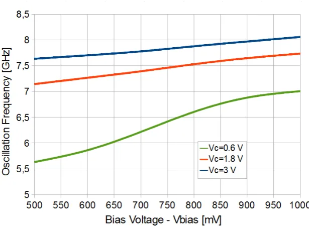
4.2 Oscillation frequency and output power vs. Control Voltage (Vc) forVbias = 900mV 63 4.3 Current consumption vs. bias Voltage forVc= 1.8V . . . 64
4.4 Oscillation power vs. Bias Voltage forVc= 0.6V,1.8V,3.0V . . . 64
4.5 Oscillation Frequency vs. Bias Voltage forVc= 0.6V,1.8V,3.0V . . . 65
4.6 7GHzIC wirebonding to the measuring PCB . . . 65
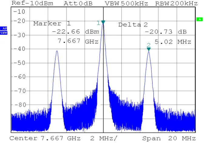
4.7 Output spectrum of the VCO perturbed by a substrate coupled noise at a 5M Hz frequency offset from the carrier . . . 66
4.8 Spur amplitude for different frequency offsets . . . 66
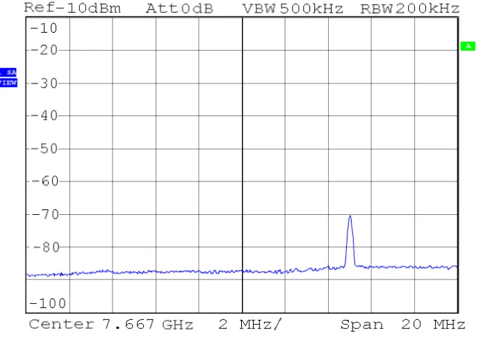
4.9 Output spectrum with HFSN injected and the VCO not oscillating . . . 67
4.10 Comparison between the sideband amplitude with and without VCO oscillation . . . 68
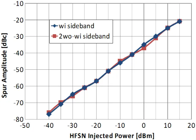
4.11 Comparison between the sideband amplitude and the HFSN amplitude . . . 68
4.12 Output spectrum of the HFSN perturbed VCO showing the occupied bandwidth of each of the sidebands . . . 69
4.13 Comparison between the sideband relative amplitude and the VCO oscillation am-plitude . . . 70
4.14 Oscillator Injection locking effect diagram. . . 72
4.16 Measured output spectrum of the LC-VCO for different offset frequencies . . . 75
4.17 Measured locking range for different substrate noise power . . . 76
4.18 Diagram of the output spectrum of an narrow band FM modulated signal. . . 77
4.19 Diagram of the mirror sideband generation for the maximum and minimum LC-VCO oscillation frequencies . . . 79
5.1 Block diagram of a resonant based oscillator . . . 84
5.2 Schematic of a typical NMOS LC oscillator . . . 84
5.3 Magnitude and phase of the tank impedance. . . 85
5.4 Definition of quality factor from a bandwidth point of view . . . 86
5.5 Phasor representation of the oscillator signal . . . 89
5.6 Example of the frequency change in the tank caused by the phase shift. . . 90
5.7 Bessel function of the first kind for the first five orders . . . 96
5.8 Ideal LC-oscillator with noise sources at the tank . . . 101
5.9 Ideal LC-VCO with current noise sources . . . 102
5.10 Norton and Thevenin transformation of the HFSN source. . . 102
5.11 Oscillation Frequency with noise (blue trace) and without noise (red trace) . . . 103
5.12 Comparison between the simulated and the model predicted relative sideband amplitude107 5.13 Comparison between the simulated and the model predicted relative sideband amplitude110 5.14 Relationship between biasing current and oscillation amplitude . . . 113
5.15 Comparison between the simulated and the model predicted relative sideband amplitude113 5.16 Relationship between the tank resistance, the biasing current and the tank quality factor115 5.17 Comparison between the simulated and the model predicted relative sideband amplitude117 5.18 Comparison between the simulated and the model predicted relative sideband amplitude120 6.1 Structure of the 2.5 GHz QVCO . . . 124
6.2 Diagram of the frequency divider input and output signals. . . 125
6.3 Schematic of the 5 GHz LC-VCO . . . 125
6.4 LandQLmeasurements, together with the inductor layout. . . 127
6.5 Structure of the frequency divider. . . 129
6.6 Schematic of one of the frequency divider latches. . . 129
6.7 Typical sensitivity curve of a CML frequency divider. . . 130
6.8 Measured sensitivity curve of the divider designed in this work. . . 132
6.9 Micro photography of the manufactured QVCO . . . 133
6.10 Output spectrum of the LC-VCO with an injected 5 GHz HFSN . . . 134
6.12 Effect of 2.5 GHz HFSN on the frequency divider . . . 136
6.13 Occupied bandwidth of the carrier and the sidebands before and after the divider . . . 137
6.14 Calculated occupied bandwidth of the carrier and the sidebands before and after the divider . . . 139
6.15 Generic model of a real CMOS inductor [130] . . . 141
6.16 Relationship between the NM3 gate voltage, the biasing current and the LC oscillator amplitude. . . 143
6.17 LC oscillator amplitude and sideband amplitude for different biasing current values. . 143
6.18 Spectrum of a frequency modulated signal (left) and of the same modulated signal after a times 2 frequency divider (right). . . 144
6.19 Output spectrum of the 5 GHz LC-VCO affected by HFSN . . . 146
6.20 Output spectrum of the 2.5 GHz QVCO affected by HFSN . . . 146
7.1 Layouts of the grounded shield (left) and floating shield (right) inductors . . . 151
7.2 Simulated isolation between the substrate and the inductors. . . 152
7.3 Test chip microphotograph and simplified schematic. . . 153
7.4 Effect of HFSN on the instantaneous oscillation frequency and output spectrum. . . . 154
7.5 Relationship betweenVcand the sideband spur amplitude caused by HFSN on both VCOs. . . 154
7.6 Relationship betweenVbias and the sidebands’ relative amplitude caused by HFSN in both VCOs. . . 155
7.7 Varactor capacitance and quality factor as functions of the control voltageVc. . . 157
7.8 Tank quality factor of the grounded and floating VCOs. . . 157
7.9 Oscillation amplitude of the grounded and floating VCOs. . . 158
7.10 Relationship between oscillation amplitude, current consumption, and Vbias on the grounded and floating VCOs. . . 159
7.11 Oscillation frequency of the grounded and floating VCOs. . . 159
7.12 Relationship between Vc and the sideband spur amplitude predicted by model and simulation of both VCOs. . . 161
7.13 Relationship between oscillation amplitude and sideband amplitude predicted by model and simulation. . . 161
7.14 Scheme of the experimental set-up for the measurement of HFSN effects on the VCO output. . . 162
7.15 Measured sideband relative amplitudes for different frequency offsets. . . 163
7.16 Measured spur amplitude for the grounded and floating VCOs . . . 163
List of Tables
1.1 Market and Financial issues comparison between SiP and SoP . . . 3
1.2 Technical features comparison between SiP and SoP . . . 3
3.1 Reported isolation values between two ports. . . 42
3.2 Reported isolation added by P+ grounded guard rings around the victim port. . . 43
3.3 Reported isolation added by a triple well isolating the victim port. . . 44
4.1 Frequency and amplitude of the generated second and third order harmonics. . . 71
5.1 Base component values of the presented LC-VCO . . . 103
5.2 Comparison between simulation and model prediction . . . 104
5.3 Simulation results of the effect of the frequency offset . . . 105
5.4 Comparison between simulation and model results of the effect of the frequency offset 106 5.5 Simulation results of the effect of the tank noise amplitude . . . 108
5.6 Comparison between simulation and model results of the effect of the tank noise amplitude . . . 109
5.7 Simulation results of the effect of the oscillation amplitude . . . 111
5.8 Comparison between simulation and model results of the effect of the oscillation amplitude . . . 112
5.9 Quality factor, bias current and oscillation amplitude for different values of the par-allel tank resistance . . . 114
5.10 Simulation results of the effect of the tank quality factor . . . 115
5.11 Comparison between simulation and model results of the effect of the parallel tank resistance . . . 116
5.12 Parallel tank resistance, bias current and oscillation amplitude for different values of the oscillation frequency . . . 118
5.13 Simulation results of the effect of the oscillation frequency . . . 119
5.14 Comparison between simulation and model results of the effect of the oscillation frequency . . . 119
6.2 Summary of the measured 2.5 GHz QVCO characteristics and performance . . . 133
Abbreviations
AC Alternating Current
BER Bit Error Rate
CMOS Complementary Metal-Oxide Semiconductor
CAD Computer Aided Design
CML Current Mode Logic
DC Direct Current
EM Electromagnetics
ED Electro Dynamic
EQS Electro Quasy Static
FDM Finite Difference Method
HFSN High Frequency Substrate Noise
HDMI High Definition Multimedia Interface
IEEE Institute of Electrical and Electronics Engineers
LNA Low Noise Amplifier
mmW millimeter Wave
NMOS Negative Metal-Oxide Semiconductor
PGS Patterned Ground Shield
PLL Phase Locked Loop
PMOS Positive Metal-Oxide Semiconductor
PA Power Amplifier
PCB Printed Circuit Board
QVCO Quadrature Voltage Controlled Oscillator
RF Radio Frequency
SiP System in Package
SoC System on Chip
Chapter 1
Introduction.
1.1
Thesis scope and motivation
During the last years, the basic physical limits of the CMOS scaling are restricting the evolution trends of the CMOS integration. The Moore’s Law is starting to be limited by the fact that reducing the size of a transistor does not necessary imply an improvement in terms of power consumption, size, performance and even price. The CMOS industry has been investing during the last years in the improvement of the system level integration as a path to continue with the improvement in cost, size and performance that the conventional CMOS scaling alone is not able to provide. The complete System-on-chip (SoC) IC integration (see Fig.1.1 left) is the main goal of nowadays semiconductors industry, which is always focused in “getting more functionality at an affordable cost”, according to Rao Tummala [1], one of the main researchers about system integration.
when a reduced number of dies is used, as the reusability of IPs and the capability of upgrading indi-vidual components, both critical in shorting the so important time-to-market. In summary, in terms of just performances the best solution uses the minimum possible number of dies (being the SoC the ideal paradigm), but in systems where there is no high volume production or with tight time-to-market requirements the optimum number of dies increases. In any case, it is clear that the complete atomization of a design into a large number of dies is also far from being the best solution and a high effort should be done to cope with the few dies/SoC drawbacks.
Figure 1.1. Typical SiC and SoP structures
One of the expanding fields in which the SoC paradigm has exploited its strengths and potential benefits, is the implementation of communication systems for portable applications. The integra-tion of wireless radiofrequency transceivers –physical layer– together with data processing network management and data processing in the digital domain, all in a single silicon die, enabled low-cost, low-volume and low power solutions for communication systems that boosted the appearance of all kind of portable gadgets, the well known mobile revolution that started in the early 2000’s and that today keeps changing our daily life and the global economy.
The first SoC solutions appeared in the early 2000’s for low-demanding communication stan-dards, like the SoC shown in Fig.1.2(a), implementing the Bluetooth V1.0 specification at a 1M bps
rate, -80dBmsensitivity and +2dBmoutput power [3]. In subsequent years, SoCs for IEEE 802.11n WLAN communication standards ( [4], Fig. 1.2(b)), telephony ( [5], Fig.1.2(c)), or positioning ( [6], Fig.1.2(d)) were developed, achieving increasing performance in terms of data rate, sensitivity or transmitted power.
Market and Financial Issues
Item SiP SoC
Relative NRE cost 1X 4X to 10X
Time to Market 3 to 6 months 6 to 24 months
Relative Unit Cost 1X 0.2X to 0.8X
Table 1.1. Market and Financial issues comparison between SiP and SoP
Technical Features
Pros
SiP SoC
Can combine different front end technologies; GaAs, InP, Si,
SiGe, etc.
Better yields at maturity (this depends upon
complexity)
Can combine different device generations Greater miniaturization
Re-use of common devices Improved performance
Reduced size vs. conventional packaging Lower cost in high volume
Active and passive devices can be embedded CAD systems automate interconnect design
Individual components can be upgraded Higher interconnect density
Better yields for smaller chip sets Higher reliability (not true for very large die)
Individual chips can be redesigned cheaper Simple logistics
Noise and crosstalk can be isolated better
Cons
SiP SoC
More complex assembly Difficult to change
More complex procurement and logistics Product capabilities limited by chip technology
selected
Power density for stacked die may be too high Yields limited in very complex, large chips
Design Tools may not be adequate High NRE cost
Signal integrity in interconnects Noise interaction between blocks
harmful effects that a digital block or a mixed-signal block can have over, for example, a delicate RF or Microwave receiver, where the digital switching noise propagated through the common silicon substrate can easily overwhelm the extremely low signals that are processed by the RF blocks for a minimum sensitivity.
One of the RF blocks that is very sensitive to the noise in the substrate is the Voltage Controlled Oscillator (VCO), that implements the local oscillator with channel-tuning capability, necessary in heterodyne and homodyne architectures. The presence of noise in the substrate can harm the VCO performance in terms of output spectral purity, phase noise and it can even modify the oscillation frequency, having an important impact in the correct behavior of the rest of the blocks connected to it and the overall system performance. It is important to note that not only the noise coming from a digital circuit can have an effect on the VCO. Other RF blocks of the same transceiver can play an important role in the noise injection on the substrate, like for example a Power Amplifier that will normally inject noise at a frequency very close to the VCO fundamental output frequency.
It is expected that problems caused by high frequency noise propagating through the substrate will worsen as the technology scales and frequencies exceed the RF range and enter the millimeter wave range (mmW). Capacitive couplings gain relevance and noise transmission through the sub-strate is easier, given the decreasing impedance of silicon at those frequencies [7]. Moreover, most of the typical measures to isolate the sensitive blocks from HFSN (High Frequency Substrate Noise) lose their efficacy or are difficult to implement in the millimeter band [8], [9].
(a) SoC implementing the Bluetooth V1.0 specification
[3].
(b) SoC implementing the IEEE 802.11n Wireless
LAN specification [4].
(c) Single chip cellular radios for GSM, GPRS, EDGE
implementation [5].
(d) GPS SoC implementation [6].
1.2
Thesis objectives
The main objective of this thesis is to provide designers with models, design criteria and method-ology to design LC-VCOs robust to high frequency substrate noise. These methods and tools should be supported by a solid base, both from the empirical and theoretical point of view. The solutions provided to the designer need to be feasible and practicable and the trade off and consequences on the LC-VCO performance should be anticipated.
In order to define these methods that can efficiently reduce the effect that the high frequency substrate noise has on the VCO it is important to deeply analyze the following issues:
• Noise propagation: How does the noise propagate through the substrate?
• Effect of the HFSN on the oscillator and coupling mechanisms: Which is the effect of the noise on the performance of the oscillator? Which parameters of the noise and of the oscillator determine the level of performance degradation? Which are the main coupling mechanisms from the substrate to the VCO and which are the factors that determine the level of coupling (noise frequency, transistor dimensions, layout characteristics. . . )?
• Modeling the effect of HFSN on the LC-VCO: Is it possible to correctly model the effect of HFSN on the LC-VCO? Can this model be based on physical design parameters of the noise or of the LC-VCO (noise frequency/amplitude, transistor dimensions, layout characteristics. . . )? How accurate and which are the limitations of this model?
1.3
Thesis structure
1.4
Thesis contributions
The investigation phase of this thesis has led to the publication of several scientific papers in journals and international conferences. Those publications are listed here.
Journals:
Marc Molina, Xavier Aragon`es, Diego Mateo, Jos´e Luis Gonz´alez,”Inductor shielding strate-gies to protect mmW LC-VCOs from high frequency substrate noise.”, Microelectronics Journal; vol. 44 issue 5, pp. 405–413 , May 2013.
M. Molina, D. Gomez, X. Aragon`es, D. Mateo, and J. Gonz´elez,”Design of a 2.5GHZ QVCO robust against high frequency substrate noise.”Microwave and Optical Technology Letters, vol. 53, no. 7, pp. 1632–1637, July 2011.
International conferences:
M. Molina, X. Aragon`es, D. Mateo, and J. Gonzalez, ”Effect of high frequency substrate noise on LC-VCOs.”in Circuits and Systems (MWSCAS), 2010 53rd IEEE International Midwest Symposium on, pp. 157–160, aug. 2010. Awarded one of the best 10 student papers in the conference.
J. Gonz´alez, X. Aragon`es, M. Molina, B. Martineau, and D. Belot, ”A comparison between grounded and floating shield inductors for mmW VCOs.”, ESSCIRC, 2010 Proceedings of the, pp. 250–253, sept. 2010.
M. Molina, X. Aragon`es, J.L. Gonz´alez,”Experimental analysis of substrate isolation tech-niques for RF-SOC integration.”, SOC Conference, 2009. IEEE International, pp. 199–202, sept. 2009.
Marc Molina, Didac G´omez, Jos´e Luis Gonz´alez, Diego Mateo, Xavier Aragon`es,”Ultra low power QVCO for the 2.5 GHz ISM band using a 5GHz LC VCO with a frequency divider.”, XXIII Design of Circuits and Integrated Systems Conference, pp. 1-6. Grenoble (France), November 2008.
Chapter 2
Review of previous work on substrate
noise and its effect on LC-VCOs.
2.1
Substrate propagation and substrate modeling
During the last decade, high resistivity substrate has become a standard for RF-CMOS processes due to, among other issues, the possibility to integrate high quality passives required for RF applica-tions and the reduced noise transmission. The analysis of the noise propagation on a high resistivity substrate presents much more complexity than in a low resistive substrate with a high resistive epi-taxial layer, where the substrate can be simplified to as single electrical node [13]–[16]. In a high resistivity substrate, the noise currents are distributed through the whole volume of the substrate, not only in the surface, increasing the complexity of the propagation models. In order to properly simulate the effect that the substrate noise can have over a victim block, it is necessary to include the substrate model in the circuit level simulation. To obtain a reliable model of the noise propagation between different parts of the circuit and to guarantee the proper circuit level simulator integration, the substrate model must have a port for every substrate place where noise can be injected by an aggressor and for every single place where noise can couple to a victim.
reduce the complexity of the model obtained, the generated RC network should be approximated by a smaller circuit that exhibits equivalent electrical behavior. The reduction process has to guarantee that the reduced model retains the accuracy of the original model but containing orders of magnitude fewer circuit nodes [19], [21].
Figure 2.1. Substrate modeled as a collection of square cubes (left). Resistances and capacitances around a mesh node (right) [19].
The complexity of the network can be further simplified in those designs where the intrinsic ca-pacitance of the substrate can be ignored, which is a reasonable assumption for operating frequencies of up to a few gigahertz and switching times less than about 100ps. In this case, the 3-D resistive mesh can be reduced to an equivalent set ofn·(n+ 1)/2resistances interconnecting the n ports [22], [23]. A different approach to model the substrate consists in the use of the Green’s equations [24] to obtain an analytical expression to model the impedance between thenports instead of discretizing the whole structure. This method ends up with a much simpler matrix that can also be treated by a reduction process or can be modeled using lumped elements.
Both the FDM and Green equation approaches have been used to develop commercial substrate extraction tools1that are now commonly used to obtain models of the substrate parasitics to be in-cluded in post-layout simulations. Substrate extraction tools provide a convenient way to evaluate interactions between components in circuits with reduced number of elements, such as the interac-tions between different circuit blocks in a RF transceiver. When the substrate noise is produced by the activity of digital circuits, the problem is then the estimation of such generated noise, as well as
1
the huge number of ports required in the substrate model. In those cases, given the analog nature of the electrical noise, an analog simulation of the complete digital circuitry -as well as package and power distribution parasitics, to evaluate SSN- is ideally required, with ports at each of the compo-nents and contacts that interact with the substrate. Since such simulation is usually unfeasible even with fast-spice simulators, several macro-modeling methodologies have been developed in the last decade [25]–[27] in order to efficiently estimate the substrate noise from the generation side in digital circuits.
Figure 2.2. Cross section of a test structure with RC equivalent circuit for modeling substrate cou-pling [20]
These lumped element models provide a very comprehensive way to model the substrate but are limited to model the interaction between the ports. When some information regarding current distribution or voltage potential inside the substrate is required, 3-D electromagnetic simulators like HFSS [28], momentum [29] or IE3D [30] should be used.
the manifestation of surface waves characteristics. For extremely high frequencies, around millime-ter wave, some authors propose some electrodynamic (ED) methods to model the substrate [32]–[34] based on Poisson’s and Green’s equations.
Figure 2.3. Voltage magnitudes from the ED and EQS computations at four different frequencies. (a) f = 2GHz(b) f = 15GHz(c) f = 30GHz (d) f = 60GHz[31].
2.2
Effect of substrate noise on LC-VCOs
A more academic approach consist in the injection of a pure tone through a pad connected to the substrate [10], [11], [35], [36]. This kind of analysis makes it easier to evaluate the cause-effect relationship between the injected noise and the VCO impact, allowing the isolation and evaluation of the coupling mechanisms. This approach also imitates realistically the effect that other RF blocks integrated in the same die, like a power amplifier, can have on the VCO.
This section will review previous works that analyze the effect on VCOs of substrate noise gen-erated by three different sources: digital switching noise, low frequency analog noise and high fre-quency analog noise.
2.2.1 Effect of digital switching noise on LC-VCO performance
The characteristics of the injected noise into the substrate have a high dependence with the switching characteristics of the digital blocks [35], [37], [38], like for example, switching frequency, switching slope or synchronization. Fig.2.4 shows the substrate injected noise spectrum generated by a digital circuit for two clock frequencies and compares it with the noise floor measured when the digital circuit is not enabled. In this figure, the two terms of the noise spectrum can be clearly observed: a train of impulses at multiples of the clock frequency and a continuous component. The continuous component of the noise is caused by the random component of the digital switching and its amplitude grows with the clock frequency. Fig.2.5 shows how the impact of this continuous term coupled to the VCO severely degrades its phase noise by more than 10dBson the complete range of frequencies. This effect worsens as the digital clock frequency is increased.
Figure 2.5. Experimental results of the measurement of the impact of digital substrate noise on the VCO [35].
Fig.2.5 also shows some spurs in the degraded phase noise. The same effect is also shown in Fig.2.6, which shows another example for a clock frequency on the digital block fclk = 10M Hz. Many spurs appear around the oscillator fundamental frequency. These spurs are caused by the substrate noise coupled to the different parts of the LC-VCO, like the analog ground, the VCO active devices and passives local substrate nodes. The various spurs appearing in Fig.2.6 are labeled according to its origin. Group B come from low frequency substrate noise harmonics up-converted from close to DC to close to the VCO output frequency due to indirect AM to FM modulation. Group A and group C come from high frequency substrate noise harmonics converted from around the VCO fundamental frequency to phase noise sidebands.
Figure 2.6. Effect of the substrate injected digital noise on the VCO Phase Noise [10].
noise, on the performance of a PLL are analyzed in [39]–[42]. Fig.2.7 shows how the substrate noise can impact the jitter of the PLL due to the VCO phase noise degradation. It is obvious that the degraded phase noise of the VCO and the increased jitter of the PLL will have a direct effect on the performance of the complete system reducing SNR or increasing the BER.
Figure 2.7. Demonstration that substrate noise generates PLL jitter. Left: PLL output with no substrate noise applied. Right: PLL output with substrate noise applied [39].
2.2.2 Effect on the LC-VCO performance of a low frequency tone in the substrate
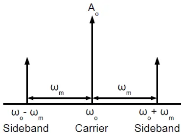
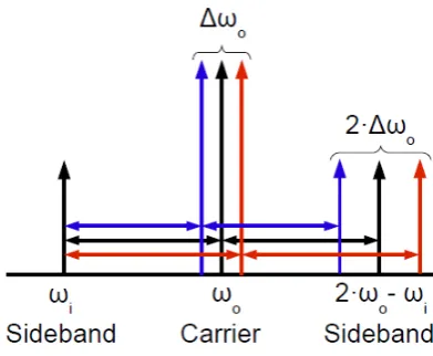
The consequences of the injection of a low frequency single tone in the substrate have been widely analyzed [10], [11], [35], [36]. All these analysis show how the coupling of this tone into the VCO generates two sidebands around the fundamental VCO output frequency, see Fig.2.8. The offset frequency of the sidebands is determined by the frequency of the tone and it is independent of the oscillation frequency. The amplitude of the sidebands is determined by several factors, like the coupling mechanisms, the distance between the aggressor and the victim or the amplitude and frequency of the tone. The analysis of the amplitude can help to determine the coupling paths of the noise to the VCO.
The two sidebands are caused by the frequency modulation of the VCO output signal due to the noise [43]. Noise couples through several ways into the VCO tank and changes the DC operating point of the tank, changing the voltage across the varactor that controls the oscillating frequency and consequently changing the oscillation frequency at the rate of the noise.
There are several different options for the noise to reach the oscillator from the substrate [36]:
Figure 2.8. VCO output spectrum with spurious tones due to 15dBm, 5M Hznoise tone [36].
• Capacitively through the n-well of the accumulation mode n-MOS varactor, to the varactor bulk node.
• Coupling to the backgates of the transistors. Resistively to the n-MOS transistor and capaci-tively through the n-well to the p-MOS transistor.
• Resistively and capacitively coupling to the non-ideal metal ground lines or ground planes.
Each of these coupling mechanisms can contribute to the LC-VCO degradation but there is a second very relevant term in this contribution, the level of sensitivity of the LC-VCO to each coupling mechanism. For example, a very low amplitude noise signal in one node may degrade the LC-VCO much more than a high amplitude noise signal in a different node.
When a sinusoidal substrate noise signal of amplitudeAnoiseand frequencyfnoise reaches the oscillator, the output signal is modulated in frequency [12], [44]. The output voltage can be expressed as:
Vout(t) =ALO·cos 2πfLOt+ 2π n X
i
Ki(vtune) Z t
0
(hisub·Vsub)(t)dt) !
(2.1)
whereALO represents the oscillator amplitude andKithe sensitivity of the oscillator frequency
hisubis the transfer function from the point where substrate noise originates, to the reception point i in the VCO.Vsubrepresents the sinusoidal noise signal traveling through the substrate.
Since the substrate noise signals are small compared to the local oscillator signal, narrow-band FM can be assumed and the expression for the amplitude of the sidebands tones at the VCO output becomes [44]:
|Vout(fc±fnoise)|= n X i
Hsubi (fnoise)Ki(Vtune)AcAnoise 2fnoise (2.2)
Experimental results [12], [35] have shown that the coupling to the inductor and the coupling to the ground are the two most relevant coupling mechanisms between the substrate and the LC-VCO due to their high sensitivity and high coupling from the substrate. Equation (2.2) can then be simplified to these two components.
|Vout(fc±fnoise)|=
AcAnoise 2fnoise
h
HsubGnd(fnoise)KGnd(Vtune) +HsubInd(fnoise)KInd(Vtune) i
(2.3)
Several investigations have been carried out to analyze, simulate and define the effect and cou-pling paths of low frequency noise into the VCO. It has been widely agreed [12], [36], [43], [45] that the non ideal ground is one of the main paths between the VCO and the substrate. When the noise in the substrate reaches the ground of the circuit, it can create ground bounce due to the parasitic resistance of the GND metal as well as the bonding and package parasitic inductance. This effect is presented in [36], where the coupling of the noise to the ground power lines is analyzed as one of the main contributor to the VCO performance degradation. The author introduces a 3.5GHzVCO with the possibility of injecting a noise tone directly into the substrate. The VCO performance is analyzed in the noise frequency range from DC to 15M Hz, showing the impact of the resistive coupling of noise from the substrate to the non-ideal on-chip ground interconnect, resulting in analog ground bounce and frequency modulation.
frequency-independent. The inversely proportional relation between spur amplitude and the substrate noise frequency proves that this is resulting from a resistive coupling (flat in frequency) followed by fre-quency modulation (-20 dB/dec). At large frequencies, the capacitive mechanisms become relevant enough and dominate over the resistive ones. As the frequency-proportionality of the capacitive cou-pling compensates the1/f of the frequency modulation, the spur amplitude appears now constant versus the noise frequency.
Figure 2.9. 1/f dependence of the spur amplitude vs. the noise frequencies [35].
Experimental analysis provides a limited insight into the coupling mechanisms. Understanding with precision the main paths of coupling is essential to the circuit designer in order to undertake measures (adding isolation around specific components, for example) in order to minimize noise impact on the VCO output. Later works have combined experimentation, simulation and circuit analysis in order to provide this identification [12], [35], [44], [46]. In [36], a VCO including a realistic model of the ground network is simulated with the objective of determining the contribution of each of the coupling mechanisms. In this case, only resistive ground connections, NMOS transistor bulk and capacitive coupling to the inductor are analyzed. Fig.2.10 is a graphical representation of the simulation method showing, the substrate noise propagation, the coupling mechanisms taken into account and the interconnect metal network.
modulation of the local oscillator frequency. Impact via the inductor is significantly lower because it results from capacitive coupling which is negligible for the studied substrate noise frequencies. Impact via the NMOS back-gate is also inversely proportional to the noise frequency but small com-pared to the impact via the non-ideal ground interconnect .
Figure 2.10. Presented simulation method to allow the analysis of impact of the substrate noise through the different components in the RF circuit [46].
Figure 2.11. Contribution to the spur amplitude of each of the coupling mechanisms [46]
used to model the on-chip interconnects, the substrate and the passive components. Noise is injected at low frequency, from DC to 500M Hz. Simulation results show how, again, the ground bounce is the dominant coupling mechanisms for low noise frequency. Fig.2.12 shows the HFSS simulated electrical fields at 100M Hzand a comparison of the spur amplitude between real and ideal ground, evidencing the importance of modeling the GND and power parasitics. The main drawback of this analysis is the limited frequency of the noise signal. It would be very interesting to see how the different coupling mechanisms change for higher noise frequencies.
As a summary, low frequency analog noise traveling through the substrate degrades the perfor-mance of LC-VCO due to the coupling of this noise into the sensitive nodes of the LC-VCO. The cause of performance degradation is generally attributed by most authors to the ground bounce in the LC-VCO caused by the substrate noise. Low frequency ground bounce changes voltage across the oscillator varactor changing the oscillator frequency. As the frequency of the noise increases, the varactor can’t follow the rapid voltage changes and so, the interaction between the substrate noise and the LC-VCO should necessarily change.
2.2.3 Effect on the LC-VCO performance of a high frequency tone on the substrate
Several characteristics of the effect of substrate noise on LC-VCOs change as the frequency of the noise increases. The capacitive behavior of the substrate makes the substrate impedance lower at high frequency, allowing the noise to flow easily through it and so, reaching the victim with higher power. The substrate models become more complex and the validity of the passive network propagation models needs to be reviewed. Moreover, high frequency noise can couple capacitively from the substrate into the oscillator. A physical connection is not required and so, the analysis of the coupling paths becomes much more complex. The effects of the high frequency noise on the LC-VCO should differ from those at low frequency, as, for example, the high frequency noise cannot change the biasing DC point of the varactor. Finally, the efficiency at high frequency of the isolation techniques used for low frequency isolation is still to be confirmed. A deep analysis is required to find the difference between low and high frequency substrate noise effect.
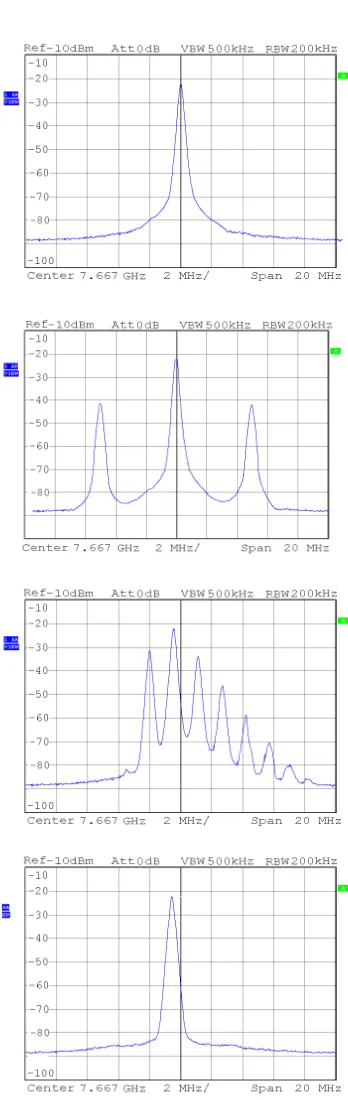
Again, experimentation is a good tool to cope with the limitations of simulation techniques at high frequency. The output spectrum of a 900M Hz LC-VCO when a sinusoidal signal with a frequency of 304M Hz is injected into the substrate is shown in Fig. 2.13 [47]. Several sidebands, caused by the effect of the noise, appear at different frequencies.
Both the effect on the LC-VCO as well as the coupling mechanisms have a very strong de-pendence with the frequency of the noise. The noise effect on the oscillator can be reviewed by measurements but identifying coupling mechanisms and paths requires advanced simulations.
Figure 2.13. Output spectrum of a 900M Hz LC-VCO with a 304M Hz frequency interference injected into the substrate [47].
• At low frequencies, sideband spurs are caused by FM modulation of the local oscillator. From DC to 10M Hzthe substrate noise signal couples resistively into the non-ideal ground lines. The spurs are decreasing with 20dB/decwith the offset frequency.
• At intermediate frequencies (10M Hzto 100M Hz) the dominant impact mechanism is mov-ing from FM to AM modulation. The amplitude of the spur starts to increase with 20dB/dec.
The main coupling mechanism is the inductor, resulting in AM modulated spurs, which ex-plains the increase of 20dB/dec.
• At high frequencies, AM modulation is the dominant impact mechanism. The substrate noise impacts increases with 40dB/dec. The external decoupling capacitors have an effect on the
coupling level.
• Close to the LO frequency, injection locking of the VCO occurs. At an offset frequency of 150M Hzfrom the LO frequency substrate noise starts pulling the LO. When the oscillator is perturbed by a substrate noise signal close to the LO frequency, the LO frequency locks to that of the perturbing signal.
This example shows the great importance the noise frequency has in the coupling mechanisms between the substrate and the oscillator.
injected in the substrate with a frequency very close to the oscillator fundamental frequency. The perturbed output spectrum shows three components: one is the fundamental VCO output, a second one is at the injected frequency and a third one appears at the opposite side of the VCO ouput at the same frequency offset as the second one. The author states that this third signal “represents an intermodulation product as a result of the nonlinearity of the VCO” citing Razavi [48] as the reference. Certainty, Razavi blames intermodulation as the cause of the second sideband in [48] but, some years after, the same Razavi publishes a new study [49] analyzing the effect of pulling in unlocked injection locked oscillators where he attributes these sidebands to the frequency modulation of the oscillator caused by the pulling effect.
Figure 2.14. 5.2 GHz VCO output with noise on and off for varying biasing current.Ilow=1.81 mA, Imid=2.71 mA,Ihigh=3.41 mA [11].
In order to investigate a more realistic scenario, a different approach can be taken by placing a real aggressor instead of an injection pad. In an RF transceiver the power amplifier can easily interact with the oscillator due to the high amplitude signals at its output and due to the three different coupling paths between the PA and the VCO: resistive and capacitive coupling through the substrate and magnetic coupling between the PA spiral inductor and the VCO spiral inductor. This situation is shown in Fig.2.16 and Fig.2.17 [50] and has been experimentally reported for example in [51], [52]. It must be noted that in [51] interaction between the VCO and the PA produced inadequate operation of the receiver even if they were placed about 3mmapart in the same silicon die.
Figure 2.16. Typical transmitter block diagram. The VCO and PA are placed close to each other. [50]
Figure 2.17. Different coupling mechanisms between a PA and an LC-VCO. [50]
The resulting output spectrum of the LC-VCO when the PA is working is shown in Fig.2.18. Several sidebands appear all along the output spectrum showing a relevant interaction between the oscillator and the power amplifier. Authors identify four different different coupling mechanisms:
• electrically through the common substrate;
• magnetically between the on-chip inductors of the PA and LC-VCO;
Figure 2.18. Spectrum of the LC-VCO operating at 5.1 GHz when the PA is excited at 3.68 GHz. [50]
• capacitively between the traces of both circuits.
In order to evaluate the level of contribution of the subtrate as a coupling mechanism, the die is cut, physically separating the PA from the LC-VCO, as shown in Fig.2.19 left. The results show a big reduction in the LC-VCO performance degradation, like shown in Fig.2.19 right. This experiment shows that, even if the magnetic coupling between the inductors is a relevant source of coupling, the substrate plays a very important role in the LC-VCO degradation.
Figure 2.19. Substrate cut test to reduce LC-VCO and PA coupling [50]. Dicing the PA from the VCO test to remove the substrate coupling (left). Measured right-sideband spur(fLO−fP A)of the
5.1 GHz LC-VCO when the PA is excited (right).
knowledge around this effect. For example, it is necessary to determine the interaction mechanisms between the HFSN and the VCO in order to be able to determine measures to protect the LC-VCO and reduce its performance degradation.
2.3
Techniques to mitigate the noise coupling
Previous section has proven that the noise can travel through the substrate, reach the LC-VCO and degrade its performance. It is extremely important to define measures to reduce this degradation. This section presents the most common measures proposed in the literature.
2.3.1 Ground plane optimization strategies
One of the conclusions obtained by some of the studies in the previous sections is that the non-ideal ground of the VCO is affected by substrate noise currents, that couple, resistively and capaci-tively, to the ground and flow through its parasitics, causing a voltage bounce. Several authors [12], [46], [53] propose the reduction of the ground plane impedance as the simplest solution to reduce ground bouncing. This solution implies the use of the thickest metal to create a ground plane around the VCO. Implementation of this type of solutions must be made carefully since they are extremely layout-dependent, thus their efficacy should be checked case-by-case. For example, if the mentioned ground plane extends close to a noise-generating circuit, the plane can provide a low-impedance path to the VCO, thus worsening the interaction instead of reducing it. On the other side, minimizing the impedance of the ground plane follows the idea of creating a ”good ground”, but this does not only depend on the on-chip grounding scheme, but also in the packaging and bonding parasitics, as the same authors recognize in later works [12].
Figure 2.20. Effectiveness of the use of a dedicated bond wire for the substrate guarding structures. No guard ring (left), guard ring with dedicated bonding (right) [54].
connected to the PCB ground using a dedicated bond wires provides around 20dBof isolation over the solution with a shared bond wire [54].
2.3.2 Substrate isolation structures
Once the noise has already reached the substrate, the designer should protect or shield the sen-sitive parts of the analog systems from the noise generated by the rest of the circuitry, both analog and digital. The basics behind this protection strategies are very intuitive: sink the noise to a clean ground before it reaches the sensitive parts of the circuit. There are several structures available which provide different levels of isolation at different frequencies. These structures can be classified in two main groups:
• Guard rings: A P+ or N+ diffusion surrounding, side by side, the substrate contact to sink the noise to ground.
• Wells: The sensitive element is placed inside of a deep well, completely surrounded by the protection structure.
Finding the optimal structure at the right frequency range with the minimum cost (in area, man-ufacturing cost or power consumption, for example) is the main challenge for the designer.
(a) Example of P+ guard ring over P substrate (b) Example of deep N+ well over P substrate
Figure 2.21. Substrate isolation structures
capacitors, like shown in Fig.2.23. Those simplified models allow the simulation of the test structures with very low computational requirements, providing a solid method to evaluate he efficiency of each of the protection structures [55].
Figure 2.22. Substrate noise test structure
The designer has also available simulation methodologies to co-simulate the effect of guard ring on mixed signal designs [56], [57] together with the 3-D electromagnetic simulators like HFSS [28], momentum [29] or IE3D [30]. The proposed simulation technique of guard ring structures can in-clude all the dependencies with geometric parameters, layout placement and vertical impurities and thus can be strongly helpful to establish isolation strategies against substrate coupling in a given tech-nology. Simulation and measurement results on their investigation (see Fig.2.24) show that the guard ring structures can provide increased isolation of tens of dBs, although with a strong dependency on the frequency and type of structure implemented.
(a) Guard ring cross-sectional view (top), proposed circuit model
(bot).
(b) Triple well cross-sectional view (top), proposed
cir-cuit model (bot)
Figure 2.23. Substrate isolation structures and their circuit level models [55]
may observe that several authors [56], [58]–[63] have reported very different results for the same structures in very similar technologies, suggesting that the substrate isolation structures can be very effective but the level of efficiency highly depends on other parameters, like for example, the quality of connection to ground or the quality of the ground itself. The main limitation of these structures is that the level of isolation drops as the noise frequency increases. The amount of available informa-tion about the efficiency of these structures beyond 10GHzis really limited. Anyway, most of these authors agree in the fact that P+ guard rings provide a very effective isolation, especially at low and mid frequencies, at a very reasonable cost (area) without the need to add very costly extra fabrication processes. For this reason, P+ guard rings are commonly used as a low cost solution to improve the substrate isolation.
Figure 2.24. Guard ring structures (a) P+ GR (b) N+ GR, (c) deep N -well GR, (d) deep N-well pocket and the simulated S21 versus frequency dependence for these structures [57].
Figure 2.25. Schematic of the sizable guard ring (left) and the transfer functions for different widths of the expandable guard ring (right) [47]
Other authors have also reported the important relationship between the quality of the ground connection and effectiveness of the isolation structures. It is extremely important to minimize the impedance of the current return path. As the frequency increases, the inductance of the return path becomes very relevant [64]. The total impedance is tied to the physical and geometrical character-istics of the layout. This is probably one of the main explanations to justify the high dispersion on the different levels of isolation provided by different authors. An example of the degradation of the isolation level due to the inductance of the isolation structure ground connection is shown in Fig.2.26.
Figure 2.26. Guard-ring isolation as a function of frequency for 0.5, 0.3, and 0.1 nH inductance of the ring ground connection versus no guard ring [64].
2.3.3 Inductor shielding
Inductors are usually the largest area components on an RF transceiver. This fact makes them one of the main possible noise paths between the circuit and the substrate because of the large capacitance, both for noise injection and noise picking. On the other hand, currents flowing through inductors create magnetic fields that can penetrate into the substrate, generating noise. Magnetic field can also induce currents on other inductors or interconnects. For all of these reasons, it is very important to take inductors into account when analyzing the coupling mechanisms between RF circuits.
The first documentation about the usage of inductor shielding as a measure to increase the iso-lation dates from 1998 [65]. In this article the authors present a Patterned Ground Shield (PGS) inserted between an on-chip spiral inductor and silicon substrate. The impact of the shield on induc-tance, parasitic resisinduc-tance, capaciinduc-tance, quality factor and substrate isolation is studied extensively. Results show that the shield increases the inductor quality factor up to 33% and reduces the substrate coupling between two adjacent inductors by as much as 25dB. Fig.2.27 shows these effects.
Figure 2.27. Effect of polysilicon PGS on Q of a 2-GHz LC tank (left) and effect of the shield on substrate coupling between two adjacent inductors. [65]
theory about the N+ diffusion layer, designing a double patterned shield using polysilicon and the N+ diffusion layer. Results show some examples where the quality factor of the inductor is increased by 50% reducing the coupled energy to the substrate more than 60%. Other investigations have also confirmed that PGSs on metal layers can provide results as good as n+ diffusion ones [67].
A widely spread investigation line is the discussion about the importance of the shield ground connection. A grounded shield can isolate the inductor from the substrate underneath but can also transmit the ground bounce from the ground network to the inductor. Thus, some authors advocate for floating shields. Moreover, a grounded shield will only be effective if it can sink noise effectively to a clean ground. A test regarding the effectiveness of the ungrounded shield is performed in [68]. Four different test structures are measured to understand the effects on the substrate isolation of each of the inductor grounding methods shown in Fig. 2.28. The comparison of the isolation measurements between the four test cases can be seen in Fig.2.29. When PGS is well grounded, the substrate noise suppression below 12GHz is more than 48dBand is much better than the one when PGS is floating. When PGS is grounded with relevant parasitics, the substrate noise suppression degrades faster at higher frequency. The conclusion of the article proposes that in order to make the design immune to substrate noise, the parasitic inductance and resistance of the on-chip ground connection of PGS have to be kept as low as possible.
Figure 2.28. Microphotograph of the inductors: (a) PGS is well grounded, (b) PGS is grounded with parasitics, (c) PGS is floating, (d) without PGS [68].
Figure 2.29. Measured isolation between inductor and substrate contact of structures presented in fig. 2.28 [68].
to the inductor winding induces no net voltage onto the shield Metal, blocking capacitive coupled currents from entering the silicon substrate, thereby reducing substrate dissipation and improving the inductor quality factor. The floating shield presents several advantages over the traditional ground shield [69], [70]. First, the floating shield does not need an explicit 0V ground reference. Second, the floating shield is not connected to, or directly driven by, AC sources such as transistors. It shields a passive device by electric induction, and can even maintain 0V on the shield at mm-wave frequencies due to the virtual ground at the center of the inductor. Moreover, the floating shields of different passive devices are not connected together, so isolation between devices is improved over grounded shields which are connected to a common on-chip ground.
Figure 2.30. Floating ground shield layout showing the virtual ground [69].
Figure 2.31. Schematic of the 60GHz VCO and floating technique used in the inductor [71].
a 60GHz VCOs [71]–[73]. Fig.2.31 shows the schematic of a VCO and the floating shield technique used for the design of the inductor [71].
The floating shield does not allow the current to flow parallel to the signal path, reducing the loss and increasing the inductance per unit of length [74]. The line is actually behaving as in free space. The strips under the line provide a shield from the substrate. This kind of transmission lines are also known as Slow Wave Transmission Lines [69], [75].
with an unshielded inductor and one with a Grounded coplanar transmission line. Fig. 2.32 shows a micro-photography of each of the VCOs and the transmission line structure.
Figure 2.32. Micro-photography of the LC-VCOs with spiral inductor (a) and shorted stub inductor (b) (left). Shorted stub inductor description (right) [77].
The results of the analysis show that although the spiral inductor is favorable in terms of quality factor and self-resonant frequency, the shorted transmission line offers superior isolation from the substrate. The solid ground shield of the transmission line offers reduced sensitivity to substrate interference. The 60GHz VCO with shorted transmission line as inductor achieves a measured 22.6dBlower spur power level (see Fig.2.33).
Figure 2.33. VCO output spectrum of the inductor-VCO (left) and the Shorted-stub-VCO (right) [77].
2.4
Summary and conclusions
Chapter 3
Experimental analysis of EM substrate
coupling and isolation techniques at RF
frequencies.
3.1
Introduction
Secondly, this chapter analyzes the role of inductors and substrate in the interaction between analog RF blocks. Isolation between inductors with different geometry and placement is analyzed, as well as the efficacy of techniques to increase this isolation.
3.2
Substrate noise coupling and analysis of the efficiency of isolation
techniques
This section analyzes the coupling between two contacts on the substrate and the effect that dif-ferent isolation techniques have on the coupling level. Several works have been published during the last years that evaluate the efficacy of different isolation techniques available in CMOS tech-nology [8], [56], [58]–[63]. Nevertheless, these works often show contradictory results as a conse-quence of the diverse conditions applied in the reported measurement setups. A broader perspective is needed, where the efficacy of the isolation techniques is compared accounting for measurement and biasing set-up conditions and frequency range of interest.
3.2.1 Experiment description
Two different ICs have been manufactured in 0.35µmand 0.18µmCMOS processes, containing test structures to experimentally characterize the isolation techniques available in each process. Each test structure consists of two P+ substrate taps separated by a 50µm or 100µm distance (pitch), acting as aggressor and victim ports, respectively. The isolation structures are implemented only around the victim port. Each port is connected to larger square pads for on-wafer RF probe access. Two-port S-parameters are measured using a network analyzer, and the effects of probes, pads and interconnect parasitics are de-embedded from the measurements. Fig. 3.1 shows the layout of one of the test structures together with a detail of the aggressor and victim ports. Each port is a P+ diffusion of 10µmx 10µm. P+ guard rings are 10µmdistant from the victim port, and N+ guard rings are 25µmdistant. Two metal lines allow connecting the rings to ground (bottom line) orVdd(top line).
In order to make fair comparisons, these traces are present in all of the test structures, even if they are not needed. TheVddbiasing voltage was introduced through DC probes placed on pads located