Thin films of arsenic sulfide by chemical deposition and formation of InAs
Texto completo
Figure


Documento similar
Click here to view linked References.. The most important point defects and defect complexes have been explored and intrinsic defect formation energies were determined [21]. To
These surface states lie in the bulk energy gap of thin topological insulators.In thin topological insulator films tunnelling between top and bottom sur- face opens a finite gap in
The newly formed FAPI-PbS QDs are dissolved in FAPI solution for the fabrication of perovskite thin films for the characterization and device applications
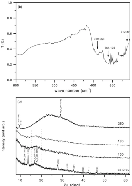
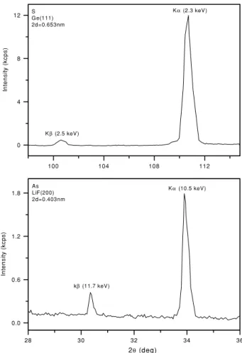
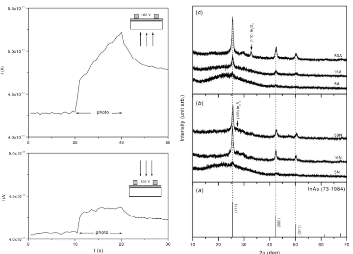
The films that exhibit p-type behavior are the films grown at lower temperatures. At the same time, the thin films obtained at these temperatures present also a
influence of these parameters on the size and distribution of Te inclusions, deep defects, optical and electrical properties of CdZnTe detectors. In the fourth chapter, the effect
12 Cross-sectional SEM micrographs and the surface morphology of CZTGS thin films show that the annealed-samples coming from the evaporation process Flash 3
Since the oxide growth rate is approximately constant along the transformation process, the oxidation time scales linearly with the nitride thickness.. This property enables
Arsenic concentration in roots and shoots of lupin plants growing
