Experimental and Simulated Electron
Microscopy in the Study of Metal
Nanostructures
Sergio Mej´ıa-Rosales and Miguel Jos´e-Yacam´an
1.1
Introduction
One of the most exciting features of nanostructures relays on the fact that matter organized as objects at the nanoscale may have chemical and physical properties different from those of the same material in its common bulk presentation. This size-dependent properties are related to several physical phenomena, such as quantum behavior, high surface-to-volume ratio, and thermal effects [1,2]. Far from being an unfortunate fact, the unique properties of nanostructures may in principle be fine-tuned to be used for a specific purpose, but to be able to dominate matter at this range of sizes, high precision tools must be used in order to investigate, measure, and modify the physical and chemical characteristics of the nanostructures. The problem is similar to the one of constructing a phase diagram for the bulk materials, but taking also into consideration size and shape, besides temperature and crystalline structure. Several groups have concentrated some of their efforts to this task (with varying degrees of success), but these attempts are inherently incomplete or, at best, restricted to one specific material and to a narrow range of sizes and temperatures [3,4]. On the other hand, these studies are generally based either on theoretical results or on indirect experimental measurements, and there is just a relatively small number of papers that concentrate on first-hand measurements of the detailed crystal structure and local chemical composition of the nanostructures. This is, to certain degree, understandable: A detailed analysis of the structure and composition
S. Mej´ıa-Rosales ()
Center for Innovation and Research in Engineering and Technology, and CICFIM-Facultad de Ciencias F´ısico-Matem´aticas, Universidad Aut´onoma de Nuevo Le´on, San Nicol´as de los Garza, NL 66450, M´exico
e-mail:sergio.mejiars@uanl.edu.mx
M. Jos´e-Yacam´an
Department of Physics and Astronomy, University of Texas at San Antonio, One UTSA Circle, San Antonio, TX 78249, USA
e-mail:miguel.yacaman@utsa.edu
M.M. Mariscal et al., Metal Clusters and Nanoalloys: From Modeling to Applications, Nanostructure Science and Technology, DOI 10.1007/978-1-4614-3643-0 1, © Springer Science+Business Media New York 2013
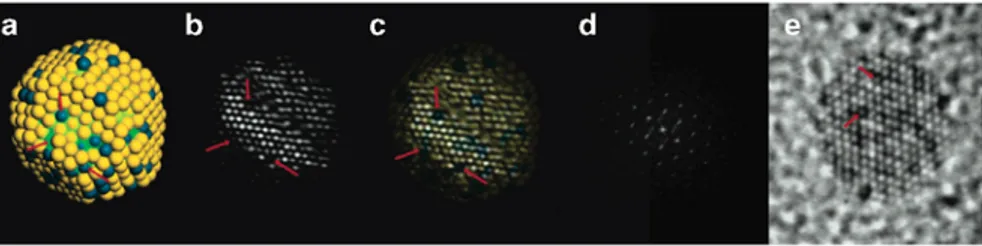
Fig. 1.1 (a) Model of AuPd particle of 923 atoms used to simulate the features of the particle
shown in (e); (b) the corresponding simulated TEM image; (c) overlap of parts (a) and (b);
(d) calculated FFT pattern for the simulated particle. In the model, blue spheres represent Pd atoms,
and yellow spheres correspond to Au atoms. Reprinted with permission from [6]. Copyright 2007 American Chemical Society
requires sub-nanometric resolution, and the electron microscopy facilities capable of reaching this resolution are not always easy to access. Besides, the interpretation of the electron micrographs is not always straightforward, since the intensity signal that correlates with the atomic positions depends not only on the length of the atomic columns parallel to the direction of the electron beam, but also on the chemical species, and on the microscope’s parameters at which the micrograph was obtained [5]. Thus, the solution to the problem of extracting a third dimension from the information contained in a strictly two-dimensional image has to be similar to the one that the human mind uses to recognize macroscopic objects sensed by the naked eye: through (a) the comparison of the observed patterns against simple models acquired by previous experience or inherited, and (b) the rough estimation of the probability of a particular model to correspond to the pattern, taking into consideration a small set of rules. An example of this use is shown in Fig.1.1, taken from [6]. Here, a TEM micrograph of a gold-palladium nanoparticle of 2 nm of diameter shows that some specific spots on the particle have a different intensity from the rest (Fig.1.1e); a model is proposed in Fig.1.1a, and a simulated TEM micrograph, shown in Fig.1.1b, is obtained. The image of the ball-and-stick model is superposed on the simulated TEM image (Fig.1.1c), and a correlation is found between the position of the spots and some specific sites at the surface of the particle, where a Pd atom is surrounded by Au atoms that are not in the same plane of the Pd atom. It is likely that these specific isolated Pd sites have a relevant effect on the chemical activity of the particle, and at least one theoretical study has investigated these kind of sites [7].
In Fig.1.1, as in the other figures where we present simulated TEM micrographs, we used the SimulaTEM program developed by G´omez-Rodr´ıguez et al. that, unlike other programs with similar purposes, allows non-periodic structures as input [8]. The principles underlying the creation of this kind of simulated TEM micrographs (and also the real ones) will be discussed in the following sections.
(HAADF-STEM) imaging, since in this technique the electron signal is strongly dependent on Z, the atomic number of the atoms that form the structure [9], which makes it the most appropriate choice for the study of metal nanoparticles.
This review does not intend to be a complete essay on the simulation of electron microscopy but a hands-on guide for researchers interested in the generation of high resolution electron micrographs of metal nanostructures. In accordance with this approach, we will only discuss briefly the working principles of electron microscopy, the role of aberration correctors, and how the theory supporting the imaging of micrographs can be used to simulate the imaging process, to concentrate later on the practical issues to be taken into consideration in the comparison and interpretation of real and simulated electron micrographs of nanostructures. The first sections give a comprehensive (but incomplete) review of the fundamental concepts related to the TEM and HAADF-STEM techniques, and to the multislice method of simulation. The remaining sections will discuss the use of real and simulated HAADF-STEM micrographs for the recognition of nanoalloys, using for this purpose several examples of shapes, sizes, and compositions.
1.2
The Transmission Electron Microscope in a Nutshell
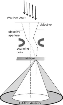
In order to study the structure of matter at Angstrom and even sub-Angstrom resolution, a beam with a wavelength on the same order of magnitude is needed. The electron microscope accelerates electrons with a potential difference of several hundreds of kV in order to produce a beam with this range of energies. In modern electron microscopes, the electrons are usually produced by a cold field-emission gun. The beam is filtered to make it practically monochromatic, and a system of condenser lenses narrows the beam divergence angle. The resulting beam interacts with the specimen, and the transmitted beam is collected by an objective lens and projected to the image plane, normally a ccd array. A simplified schematic diagram is shown in Fig.1.2.
The electron beam interaction with the sample is better understood if one considers the sample electrostatic potential or, more specifically, the projected potential of the sample. Let’s assume as a starting point that the sample is a periodic crystal, and that its electrostatic potential is described by φ(r). The projected potential will of course depend on the structural information of the sample, and also on the temperature. Then, the interaction of an electron of relativistic mass m with the sample is described by
−8πh22
m∇ 2−eφ(
r)
Ψ(r) =EΨ(r),
with the original electron wave described by a simple plane wave:
electron beam
sample
objective
objective aperture
image plane
Fig. 1.2 An overly
simplified diagram of the conventional transmission electron microscope
The solution to the Schrodinger equation will describe the electron wave function after interacting with the sample. Even with the periodicity assumption, the solution cannot be found directly without making additional simplifications. We will come back to this point in the section devoted to approximation methods of calculation.
1.3
Aberrations
Aberrations will occur, though, and this implies that not all the Fourier components of the wave function will transfer equally. The contrast transfer function (CTF) is a broadly used quantity that determines the range of characteristic spatial frequencies that can be directly interpreted in a TEM image. In other words, the CTF imposes the conditions at which “what you see is what you get.” In a concise way, the electron wave function at the image plane will be related to the CTF applied to the wavefunction just at the exit of the sample. Objective apertures will affect the CTF, as well as the spatial coherence of the electron beam and its wavelength:
CTF(k) =−sin
π
2Csλ
3k4+πΔzλk2.
Here, Cs is the spherical aberration of the objective lens, and Δzis its defocus. The special case where
Δz=−4/3Csλ
is known as the Scherzer condition, and at Scherzer defocus the CTF does not change its sign in a large spatial frequency range, and hence all distances in this range can be interpreted directly as they appear in the image [5,10]. Figure1.3
shows the plot of two CTF, calculated for two different values of Cs. Both graphs were calculated at the same voltage (200 kV). The dark blue CTF was generated
0 2 4 6 8 10
-1.0 -0.8 -0.6 -0.4 -0.2 0.0 0.2 0.4 0.6 0.8 1.0
CTF
k (nm-1)
Cs= 0.01mm
Cs= 1.2 mm
Fig. 1.4 HRTEM simulation of a cubic fcc gold nanostructure obtained at three different values of
Csaberration; (a) Toy representation of the nanostructure, and simulated TEM micrographs with
(b) 0.01 mm of Csaberration; (c) 0.1 mm of Csaberration; (c) 1.0 mm of Csaberration. All the micrographs were simulated at the Scherzer condition
Fig. 1.5 HRTEM simulations of a cubic fcc gold nanostructure calculated at different defocus
values. The image labeled as (d) corresponds to the Scherzer defocus
for a Csof just 0.01 mm, trying to simulate the conditions in a Cs-corrected TEM. In this virtual TEM, the theoretical resolution is of 0.08 nm. The light blue CTF was calculated with a Csof 1.2 mm, for comparison purposes. In this case, the theoretical resolution is 0.25 nm, not quite good for the measurement of interatomic distances. Both CTFs were obtained at Scherzer conditions. The curves were plotted using the CtfExporer software created by M. V. Sidorov [11].
The generation of TEM images at the Scherzer condition allows that atomic positions to correspond with dark spots in the micrograph, if the beam is parallel to the axis zone and the aberrations are small. The effect of aberrations in the resolution should be obvious from the CTF, but it is always interesting to see this effect directly on the images, real or simulated. A comparison of three simulated TEM micrographs is made in Fig.1.4for the same sample, a small fcc cubic volume of gold atoms. The figure shows that even at Scherzer defocus the images are difficult to interpret if aberrations are not as small as in Fig.1.4b, and that the effect of spherical aberration may appear particularly remarked at the border of the structure.
1.4
High Angle Annular Dark Field Scanning Transmission
Electron Microscope
From the point of view of the reciprocity theorem, the STEM is optically equivalent to an inverted TEM, in the sense that if the source and the detector exchange positions, the electron ray paths remain the same [10]. In the STEM, the objective lens—and all the relevant optics—is positioned before the specimen (see Fig.1.6). For the specific case of the Annular Dark Field (ADF) detector, only the electrons scattered betweenθ1≤θ≤θ2contribute to the image, since these are the electrons that reach the annular detector. Working at 200 kV (appropriate for imaging metals), in a typical HAADF-STEM microscope the inner angleθ1 of the ADF detector is set around 50 mrad, and the outer angleθ2is set around 100–200 mrad. At these range of voltages, the electrons momentum is large enough to require a relativistic treatment, and the use of Schr ¨oedinger equation to analyze the system is not completely correct without some adjustments at the values of mass and wavelength (strictly speaking, one should use the relativistic Dirac equation instead of Schr¨oedinger’s, but this would greatly complicate the already nontrivial set of equations.)
electron beam
objective
sample scanning coils objective aperture
HAADF detector
Fig. 1.6 Simplified diagram
representing the functioning principle of the
STEM differs from conventional TEM in that, unlike conventional TEM, the electron beam interacts only with a small section of the sample at a time, and the scan process is the one in charge of generating the image as a whole.
But even before taking care of the scanning issue, it is appropriate to review the different methods used to simulate the imaging process of a single area section of the sample. Some approximations are needed in each of these methods, and here we will present them in a succinct way. The reader is encouraged to review elsewhere the details of the methods and the justifications behind the approximations [10].
1.5
Approximation Methods
In the Weak Phase Object (WPO) approximation, useful for very thin samples, it is assumed that the electrons are scattered only once by the sample, so the projected potential can be averaged. When the observed sample can be regarded as a WPO, the image is linearly related to the object wavefunction. Even though this is not strictly the case in nanometer-sized structures, we will nevertheless follow this approach, and additional considerations will be taken later.
First, we can assume that the linear image approximation is valid, which means that we take as valid that the intensity g(r) on the image is obtained by a linear convolution of the ideal image of the sample f(r)with the point spread function of the microscope h(r):
g(r) =
fr hr−r dr= f(r)⊗hr−r ;
or, in reciprocal space,
G(u) =H(u)F(u).
F(u)is the Fourier transform of the specimen function, and H(u)is the CTF. The reciprocal vector u is the spatial frequency. The fact that the intensity on the image is the convolution of f(r)and h(r)means that each point in the image is a collective result of the whole of the sample.
In the WPO approximation, the specimen function is approximated by
f(x,y) =1−iσVt(x,y),
where the projected potential Vt(x,y)is very small since the sample is very thin. But
of course, this is not the case in the imaging of metal nanoparticles.
1.6
The Multislice Method
The basic idea underlying the multislice method is that the potential of the sample can be approximated by defining a number of slices of thickness dz, and projecting the potential due to the atoms of a particular slice to the central plane of this slice (see Fig.1.7).
Thus, a solution to the electron wavefunction is obtained for one slice, and used as input for the calculation of the next slice [13]. This means that the choice of very thick slices will speed up the calculations, but the potential function will be poorly approximated. On the other hand, the use of very thin slices will improve the calculation of the projected potential, but the errors due to approximations will accumulate and undermine the final result. The appropriate choice of the number of slices is an issue that requires a generous amount of effort and computing time, and the final decision must consider the benefits of a fast calculation (STEM simulations by the very nature of the technique are computationally expensive and the computing time depends on both the number of slices and the scan resolution) against the benefits of a very precise calculation (that may be critical in quantitative
Projection plane 1
Projection plane 2
Projection plane 3
Projection plane 4
Projection plane 5 slice 1
slice 2
slice 3
slice 4
slice 5
incident beam
propagated beam
propagated beam
propagated beam
propagated beam
exit beam
specimen
Fig. 1.7 The principle of the multislice method. The sample is sliced, and the potential due to the
STEM). As pointed out by Ishizuka [14], the multislice method requires several approximations that could be critical in the interpretation of results for inclined illumination, so the orientation of the sample may also affect the final result.
1.7
STEM Intensity Dependence on Atomic Number
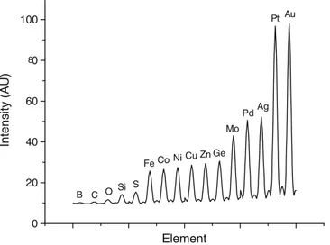
In a series of papers in the 1970s by Crewe et al., it was found that the annular detector in a HAADF-STEM microscope collects a large amount of the elastic scattered electrons, in such a way that the intensity of the signal collected by the HAADF detector will have a dependence on the scattering cross section, and thus on the atomic number of the atoms present in the sample [15]. Pennycook, one of the pioneers in the technique, gives arguments to this dependence to be close to Z3/2 (see [9]). In order to investigate how the intensity signal generated by the HAADF detector depends on the atomic number of a column formed by just one atom of a specific element, we performed a simulation of HAADF for a system of 16 isolated atoms laying on a plane perpendicular to the microscope column. The resulting image is shown in Fig.1.8, where the positions of the atoms are labeled by the symbols of their respective chemical element.
The HAADF image intensity measured over a line that passes through the center of the atomic positions is shown in Fig.1.9. Here, it can easily be noted that the contrast between heavy and light atoms is remarkably high.
The maxima in Fig.1.9are plotted against the atomic numbers in Fig.1.10, and a least squares adjustment shows that the HAADF signal follows approximately a Z1.46relation. This dependence is very close to the prediction of Pennycook.
All of the STEM simulations shown and discussed in this chapter, including the simulations presented in the next sections, were made using the commercial version of the xHREM package, a proprietary software designed and coded by Ishizuka [14]. The xHREM suite uses an algorithm based on the Fast Fourier Transform method, and it allows the use of a large number of slices, as many as 1,000 in the latest editions.
1.8
The Interpretation of an Image
Fig. 1.8 STEM-simulated micrograph showing the intensity signal due to the presence of atoms
of different elements
“The answer is that the brain supplies the missing information, information about the world we evolved in and how it reflects light. If the visual brain “assumes” that it is living in a certain kind of world—an evenly lit world made mostly of rigid part with smooth, uniformly colored surfaces—it can make good guesses about what is out there.” [16]
0 20 40 60 80
100 Pt Au
Ag Pd
Mo
Ge Zn Cu Ni Co Fe
S Si O C
Intensity (AU)
Element B
Fig. 1.9 HAADF-STEM intensity signal (arbitrary units) for several chemical elements
Fig. 1.10 STEM intensity vs. atomic number obtained by STEM simulation. The least-squared
Fig. 1.11 Upper row: Atomistic model of a cuboctahedral gold nanoparticle, and the calculated
projected potentials for each slice. Lower row: Output wavefunctions of each slice. The model was divided into ten slices, but only the nontrivial ones are presented
As it was mentioned before, the approximations used in the different simulation techniques are strictly true only when the sample is thin enough for the linear as-sumption to be correct. One of the most common approaches to implement HRTEM simulation take this assumption as the starting point, and for instruction purposes, the discussion of other difficulties will be avoided. The reader is encouraged to read the excellent text by Kirkland on this matter [10]. On the remaining of this section, we will concentrate on the use of the multislice method for the simulation of HAADF-STEM micrographs, and on the technical issues that may simplify—or make practically impossible—an interpretation of a simulated image.
1.8.1
The Problem of Slicing a Sample
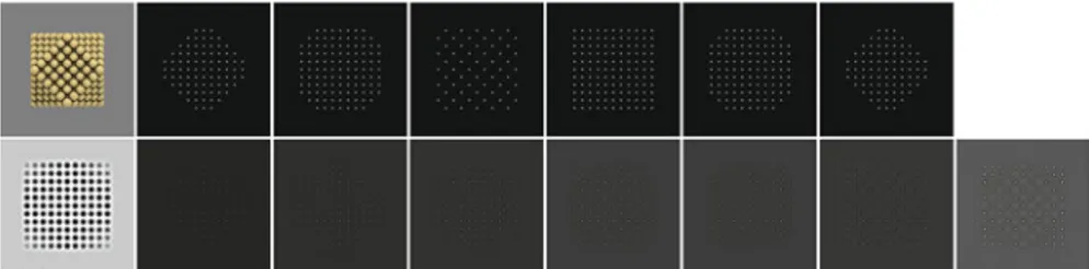
As was pointed out before, in the multislice method the sample is dissected into several slices, each treated independently through an averaged projected potential. The selection of the number of slices is a tricky job, and it will depend on the thickness of the sample (the size of the nanostructure in the case of metal nanoparticles), the orientation, and the computational capabilities. The projected potential is calculated for each slice, and the corresponding output wavefunction is obtained. Figure1.11 shows the result of the calculation of potentials and wavefunctions for a model of a gold cuboctahedral nanoparticle. The model was dissected into ten slices (only the relevant ones are represented in the figure).
If the number of slices is increased, the number of projected potentials will increase as well. This will reflect on the final result of the image, as can be seen in Fig.1.12, where a model of an icosahedral gold particle—shown in Fig.1.12a— was used to generate two simulated STEM micrographs, being the only difference between both the number of slices, 10 in (b), 20 in (c). It is not a simple task to find out which of the images follows in a better way the experimental one, since the orientation and lattice parameters must be considered.
Fig. 1.12 (a) Atomistic model of an icosahedral gold nanoparticle; (b) STEM simulation of the
nanoparticle, using ten slices; (c) STEM simulation of the nanoparticle, using 20 slices
divided into ten slices, irrespective of the model being used in the simulations. We encourage the reader interested in the multislice method to dedicate generous amounts of time to try out different slicing possibilities.
1.8.2
Orientations
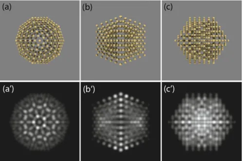
One of the first pieces of information that appear when analyzing electron mi-crographs of metal nanostructures is that there is a remarked tendency for the particles to appear with some specific geometries. The reason for this tendency is mostly energetic (apparently these geometries imply the best compromise between surface energy, conservation of crystal structure, energy of twinning boundaries, and surface/volume ratio), but it is well established that the specific geometry depends not only on the chemical constitution of the particle, but also on its size, and on the specific details of the kinetics involved in the synthesis process [2]. Typical geometries in mono and multimetallic particles include decahedra, icosahedra, tetrahedral, and cuboctahedra. How evident the shape of a particle is depends on how close is the particle to the ideal geometry, and also on the orientation of the particle with respect to the electron beam. Figure1.13exemplifies this for the case of a small icosahedral gold particle.
1.8.3
Chemical Composition
Fig. 1.13 Icosahedral gold nanoparticle at three different orientations, and their corresponding
STEM-simulated images
Fig. 1.15 Pdcore−Aushell nanoparticle at three different orientations, and their corresponding STEM-simulated images
is 30◦with respect to (a), and (c) and(c)are rotated 90◦with respect to (a). The difference in intensity between core and shell are evident.
A particle with the opposite relative concentration is used in the STEM sim-ulations shown in Fig.1.15. Here, the particle’s core and shell are not as easily distinguishable as in the previous case, since, unlike the opposite composition, the thickness of the gold regions compensates the difference in the atomic number of the elements (see Fig.1.16).
The signal generated by a true Au-Pd nanoalloyed particle is different enough from the core-shell cases to be directly identified. Figure1.17shows the results of the STEM simulations for this particle. The relative composition of this particle is close to 50%–50%, and both species are distributed randomly along the whole of the particle.
Fig. 1.16 Diagram of a
Pdcore−Aushellnanoparticle, showing that gold volume fraction explains the poor contrast between core and shell in a STEM micrograph
Fig. 1.17 Nanoalloyed Au-Pd icosahedral nanoparticle at three different orientations, and their
Fig. 1.18 (a) STEM micrograph of a Au-Co nanoparticle, shown in false colors (red: high
intensity, blue: low intensity). (b) Atomistic model used to describe the particle on (a); yellow spheres represent gold, blue spheres are cobalt, red spheres are oxygen. (c) The small squared region marked in (a) is substituted for the STEM simulation of the squared region marked in (b), and (d) the real micrograph of this region is compared against (e) the simulated one. The real and simulated line intensity profiles are also shown for comparison. Adapted from [17]. Reproduced with permission from The Royal Society of Chemistry (RSC)
to investigate the Co-Au interface; this model is shown in Fig.1.18b. The model does not intend to reproduce exactly the shape of the particle, but to give a qualitative description of the particle. Figure1.18c is a composite of the real image and a small section generated by STEM simulation; the corresponding real section is shown in Fig.1.18d, and compared against the simulated micrograph (Fig.1.18e). The two intensity profiles represented by lines in (d) and (e) are also shown for comparison. As can be seen, the simulated STEM micrograph succeeds in reproducing the main features of the real image. This result exemplifies the use of STEM simulations for an approximate description of composition and shape of metal particles.
Quantitative STEM simulation at atomic level is quite more complicated. Fluctuations in intensity on the background of a STEM micrograph can be of the same order of magnitude than the intensity generated by a single metal atom, and in multimetallic systems the problem becomes combinatorial. Nevertheless, the use of single-tilt tomography holders altogether with Cs correctors and 3D image
reconstruction algorithms allow a very precise description of shapes and structures in nanoparticles, even at atomistic level [18–20].
1.8.4
Thermal Effects
Fig. 1.19 Comparison between two simulated STEM micrographs of a cuboctahedral
nanoparti-cle. (a) Debye–Waller set to zero. (b) Debye–Waller set at 0.69
the STEM signal. It is usual to find that an electron microscopy simulation program calculate the effective form factors through the Mott formula [21]. The Debye– Waller factor is not necessarily the same at the nanoscale than the bulk value. Buffat [22] measured a decrease in the Debye–Waller factor in gold particles ranging from 0.85 in 20 nm particles, to a value of 0.69 in 2 nm particles. We used this value to simulate a gold cuboctahedral particle and compare the result against a simulation where the Debye–Waller factor was set to zero. Both images are shown in Fig.1.19. As can be noted, the thermal effects may be a determining factor on the contrast in ultra-high resolution STEM micrographs, and should not be underestimated.
1.8.5
Interatomic Distances
Fig. 1.20 (a) Sub-Angstrom resolution FePt icosahedral nanoparticle. (b) Interplanar (111)
distances vs. position of shell (shell 0 is the external shell). (c) TEM simulation of model nanoparticle. In order to reproduce the measurements of the interplanar distances, the distribution of Pt must follow the percentages shown in (b). Reprinted with permission from [23]. Copyright 2009 American Chemical Society
the size of a spot that represents a single atomic column is on the same order of magnitude as the interplanar distance itself. High resolution STEM simulations can be used to verify the experimental measurements, if an appropriate atomistic model is taken for granted. Consider for example the case of FePt icosahedral nanoparticles [23], as the one shown in Fig.1.20. FePt nanoparticles with sizes on the range of [5,6] nm were produced by an inert gas condensation, which implies that there is no passivation agent on the surface of the particles. Their structure was analyzed as icosahedral with shell periodicity. The sub-Angstrom resolution was achieved by focal series reconstruction, and it was enough to extract the position of individual atomic columns with a precision of about 0.002 nm, and to measure shell spacing differences of 0.02–0.03 nm. The measurements showed that the external shells of the nanoparticle were more spaced that the inner ones, a trend that could be interpreted as a consequence of the segregation of Pt to the external shells (see Fig.1.20b). Comparative Molecular Dynamics calculations used jointly with electron microscopy simulations (Fig.1.20c) confirmed that the structural relaxations could be attributed to Pt segregation at the outer shells generating a specific concentration gradient.
1.9
STEM, Geometrical Phase Analysis, and Its Range
of Validity
this is the decahedron, that in order to exist as a closed structure formed by five tetrahedra, it has to deform its atomic lattice, originating internal strain. A com-monly used method to measure strains directly from high resolution micrographs is the one called geometric phase analysis, or GPA in short [24]. The method, which in principle can be applied to any image with two or more sets of periodicities, is based on the local measurement of amplitude and geometric phase in reciprocal space, i.e., by the measurement of the displacement of lattice fringes in the Fourier transform of the image. There exist free and paid versions of the GPA code, both implemented to work as add-ons of the DigitalMicrograph suite [25]. The measurement procedure, in a nutshell, is as follows: (1) The power spectrum of the image (the squared modulus of the Fourier transform of the micrograph) is calculated; each periodicity present in the image will generate a bright spot in the power spectrum, and the dispersion of the spot will be at least partially due to variations in the structure. (2) A region of interest enclosing a particular bright spot is selected; this will be the reciprocal area where the phase variations will be measured. (3) The phase image is calculated following the relation
Pg(r) =−2πg·u(r),
where g is the reciprocal vector that defines the periodicity. (4) A reference area is chosen, and the phase image is recalculated, referenced to this area. The ideal reference area must be a region where the periodicity is not distorted, i.e., where the non-referenced phase image does not change abruptly. (5) The process is repeated for a second region of interest, since two sets of lattice fringes are needed for the calculation of strains. The displacement vector is expressed in terms of the base vectors defining the two periodicities:
u(r) =− 1
2π[Pg1(r)a1+Pg2(r)a2],
where
gi·aj=δij.
(6) The strain tensor is calculated:
εij=
1 2
∂ui
∂uj+
∂uj
∂ui
,
and (7) rotations of the lattice are calculated:
ωij=
1 2
∂uj
∂xi −
∂ui
∂xj
.
Fig. 1.21 (a) TEM micrograph of a fivefold gold nanoparticle. The scale bar is 10 nm long. (b) Shear strain map obtained by geometric phase analysis. Adapted by permission from Macmillan
Publishers Ltd: [26], copyright 2007
image obtained with a Tecnai F20 ST (FEI) microscope. The results are shown in Fig.1.21.
They found that, in order to close the 7.35 degree gap left by five perfect tetrahedra, each tetrahedron is strained nonhomogeneously (see Fig.1.21b).
Is it possible to use STEM micrographs to generate strain maps by GPA? It would be interesting to give it a try, since the contrast in STEM may be as good as or even better than that of conventional TEM, and the interpretation of STEM is more direct than the interpretation of TEM, but the scanning process may introduce some artifacts in the geometric analysis. This source of error can be partially overcome by aligning the scan parallel to a principal axis of strain [27], or by rotating the STEM image and then repeating the GPA process.
Fig. 1.22 (a) HAADF-STEM micrograph of a fivefold gold nanoparticle. (b) Shear strain map
obtained by geometric phase analysis
1.10
Conclusions
Electron microscopy at sub-Angstrom resolution has reached such a high level of precision that we can investigate the composition and structure of metal nanopar-ticles in an atom-by-atom fashion. This gives an invaluable capacity for the study of the interaction of metal and alloy nanostructures with biological tissue, since now it is possible to look for structure/function correlations in real time, and with a resolution high enough to investigate individual bonds. The simultaneous use of real and simulated microscopy makes the process of interpreting a micrograph more science and less craftsmanship, and gives the conclusions extracted from the measurements a more quantitative and less speculative character. Some conditions must be fulfilled to take full advantage of the top electron microscopy facilities when studying metal nanostructures: The capacity of preparing high quality samples, a fair understanding of the interaction between the sample and the electron beam, a conscious awareness of the capabilities and limitations of the different instruments and techniques, and the familiarity with different analysis approaches. And, above all, the essential element: an experienced and skillful microscopist.
Acknowledgments The authors would like to acknowledge The Welch Foundation Agency
References
1. Ercolessi F, Andreoni W, Tosatti E (1991) Melting of small gold particles: mechanism and size effects. Phys Rev Lett 66:911–914
2. Ferrando R, Jellinek J, Johnston RL (2008) Nanoalloys: from theory to applications of alloy clusters and nanoparticles. Chem Rev 108:845–910
3. Barnard AS, Young NP, Kirkland AI, van Huis MA, Xu H (2009) Nanogold: a quantitative phase map. ACS Nano 3:1431–1436
4. Ant´unez-Garc´ıa J, Mej´ıa-Rosales S, Perez-Tijerina E, Montejano-Carrizales JM, Jos´e-Yacam´an M (2011) Coalescence and collisions of gold nanoparticles. Materials 4:368–379 5. Carter CB, Williams DB (2009) Transmission electron microscopy: a textbook for materials
science. Springer, New York
6. Fern´andez-Navarro C. et al. (2007) On the structure of Au/Pd bimetallic nanoparticles. J Phys Chem C 111:1256–1260
7. Yuan D, Gong X, Wu R (2008) Peculiar distribution of Pd on Au nanoclusters: First-principles studies. Phys Rev B 78: 035441
8. G´omez-Rodr´ıguez A, Beltr´an-del-R´ıo LM, Herrera-Becerra,R (2009) SimulaTEM multislice simulations for general objects. Ultramicroscopy 110:95–104
9. Pennycook S (1989) Z-contrast STEM for materials science. Ultramicroscopy 30:58–69 10. Kirkland EJ (1998) Advanced computing in electron microscopy, vol. 250. Springer, New York 11. CtfExporer. CtfExporer (Sidorov, M. V.:).athttp://www.maxsidorov.com
12. Stadelmann P. JEMS.http://cimewww.epfl.ch/people/stadelmann/jemsWebSite/jems.html 13. Ishizuka K (2001) A practical approach for STEM image simulation based on the FFT
multislice method. Ultramicroscopy 90:71–83
14. Ishizuka K (1998) Multislice implementation for inclined illumination and convergent-beam electron diffraction. Proc Intl Symp Hybrid Anals
15. Wall J, Langmore J, Isaacson M, Crewe AV (1974) Scanning transmission electron microscopy at high resolution. Proc Natl Acad Sci USA v71: 1–5
16. Pinker S (1997) How the mind works. W. Norton & Company, New York
17. Mayoral A, Mej´ıa-Rosales S, Mariscal MM, Perez-Tijerina E, Jos´e-Yacam´an M (2010) The Co–Au interface in bimetallic nanoparticles: a high resolution STEM study. Nanoscale 2:2647 18. Gontard LC, Dunin-Borkowski RE, Gass MH, Bleloch AL, Ozkaya D (2009) Three-dimensional shapes and structures of lamellar-twinned fcc nanoparticles using ADF STEM. J Electron Microsc 58:167–174
19. Kimoto K et al. (2007) Element-selective imaging of atomic columns in a crystal using STEM and EELS. Nature 450:702–704
20. Muller DA (2009) Structure and bonding at the atomic scale by scanning transmission electron microscopy. Nat Mater 8:263–270
21. Ishizuka K (2002) A practical approach for STEM image simulation based on the FFT multislice method. Ultramicroscopy 90:71–83
22. Buffat P, Borel JP (1976) Size effect on the melting temperature of gold particles. Phys Rev A 13:2287
23. Wang R et al. (2009) FePt Icosahedra with magnetic cores and catalytic shells. J Phys Chem C 113:4395–4400
24. Hytch M, Snoeck E (1998) Quantitative measurement of displacement and strain fields from HREM micrographs. Ultramicroscopy 74:131–146
25. Mitchell DRG, Schaffer B Scripting-customised microscopy tools for Digital Micrograph (TM). Ultramicroscopy 103:319–332
26. Johnson CL et al. (2007) Effects of elastic anisotropy on strain distributions in decahedral gold nanoparticles. Nat Mater 7:120–124