Quality improvement of AlInN/p Si heterojunctions with AlN buffer layer deposited by RF sputtering
17
0
0
Texto completo
(2) Quality improvement of AlInN/p-Si heterojunctions with AlN buffer layer deposited by RF-sputtering A. Núñez-Cascajero1, S. Valdueza-Felip1, R. Blasco1, M. de la Mata2, S. I. Molina2, M. González-Herráez1, E. Monroy3 and F. B. Naranjo1 1. Universidad de Alcalá, GRIFO, Departamento de Electrónica, 28871 Alcalá de Henares, Spain Universidad de Cádiz, Departamento de Ciencias de los Materiales e Ingeniería Metalúrgica y Química Inorganica, 11510 Cádiz, Spain; & IMEYMAT: Institute of Research on Electron Microscopy and Materials, University of Cadiz, Spain 3 University Grenoble Alpes, CEA-Grenoble, INAC/PHELIQS, 38000 Grenoble, France 2. E-mail: arantzazu.nunez@uah.es. The effect of an AlN buffer layer thickness on the structural, morphological and optical properties of n- Al0.37In0.63N deposited on p-Si (111) by radio-frequency sputtering was studied. The AlN/ Al0.37In0.63N samples were structurally characterized via X-ray diffraction and high-resolution transmission electron microscopy showing that all layers present wurtzite structure highly oriented along the c-axis with no phase separation. All the samples present compact morphology with root-mean-square surface roughness below 1.7 nm and low-temperature photoluminescence emission centered at 1.8 eV. The presence of the buffer layer leads to an improvement of the structural quality, evidenced by a reduction of the full width at half maximum of the rocking curve around the (0002) AlInN reflection from 8° to 5°. Selected samples were processed and tested as solar cells showing a good rectifying behavior in the dark and an open circuit voltage of 0.35 V, a short circuit current density of 22.2 mA/cm2 and fill factor of 20% under 1 sun AM1.5G illumination.. Keywords: III-nitrides, AlInN, AlN buffer, RF-sputtering, characterization, photovoltaics… 1.. 1. Introduction.
(3) III-nitrides have attracted great interest for application in electronic, optical and photonic devices [1– 5]. In particular, the band gap of the AlxIn1-xN alloy can be tuned from 0.7 eV [6] to 6.2 eV [7] ranging the alloy composition. This material is robust against radiation, chemicals and temperature gradients [8]. However, the growth of AlxIn1-xN is challenging because InN and AlN present very different bonding energy [9], lattice parameter, growth and decomposition temperatures [10]; which lead to a large immiscibility gap in the alloy [11,12], causing phase separation and composition inhomogeneities. Metal-organic chemical vapor deposition [11,13,14], molecular beam epitaxy [15–18] and sputtering deposition [4,5,19–21] have been used for growing AlxIn1-xN layers. Among them, the sputtering technique is a low cost technology that allows the deposition of polycrystalline layers in a wide range of temperatures (from room temperature to 600°C) and on a variety of substrates (sapphire, silicon, glass, plastics…), due to the high kinetic energy of the ions involved in the growth process. The lack of substrates for growing III nitrides homoepitaxially is overcome by introducing a buffer layer which reduces the strain and prevents unwanted reactions between the III-nitride film and the substrate [22–24]. Different III-nitrides have been used as buffer layers to improve the properties of AlxIn1-xN films, being the most common GaN and AlN [5,25–29]. In this work we study the effect of introducing an AlN buffer on the quality of Al0.37In0.63N layers deposited by reactive sputtering. We present first the optimization of the growth of AlN on Si (111) substrates, tuning the radio-frequency (RF) power applied to the aluminum target. Then, we study the effect of the thickness of the AlN buffer layer on the properties of an Al0.37In0.63N film. Finally, selected n-AlInN/p-Si (111) heterojunctions were processed into solar cells and they were electrically and optically characterized. 2.. Experimental methods. The samples under study were deposited on p-doped Si (111) substrates (with a nominal resistivity 1 ̶ 100 Ω·cm) using a reactive RF sputtering system (AJA International, ATC ORION-3-HV). Before loading the substrates in the sputtering chamber, they were chemically cleaned in organic solvents and 2.
(4) blown dry with nitrogen. The targets, 2”-pure In (4N5) and 2”-pure Al (5N), were pre-sputtered with Ar (6N) prior to the growth. Once the substrates were loaded into the growth chamber, they were outgassed for 30 min at 550°C and cleaned with an Ar plasma. Then, they were cooled down to the growth temperature, achieving a base pressure of ~10−6 Pa. The N2 (6N) reactive gas was introduced into the chamber with a 6 sccm flow rate. The substrate-target distance and sputtering pressure were kept at 10.5 cm and 0.47 Pa, respectively. The growth of AlN on p-Si (111) was performed at 450°C, and the effect of the power applied to the aluminum target (150 to 225 W) on the quality of the AlN film was investigated. It has to be taken into account that the maximum theoretical power that can be applied to the Al target without inducing any damage is ~ 300 W, estimated from the magnetron dimensions (2”) and the power density tolerated by the Al target (~15 W/cm2) [30]. AlxIn1˗xN films were grown by co-sputtering the In (40 W) and Al (150 W) targets separately mounted in magnetron guns under a pure nitrogen plasma at a growth temperature of 450°C. These growth conditions result in an Al content of 37%, extracted from wavelength dispersive X-ray (WDX) measurements, and an n-type carrier concentration of n = 2.7×1020 cm-3; extracted from Hall Effect measurements [31]. More details on the deposition conditions are given elsewhere [20]. The crystalline orientation, thickness and composition of the deposited films were evaluated by high-resolution X-ray diffraction (HRXRD) measurements using a PANalytical X’Pert Pro MRD system. Atomic force microscopy (AFM) was used for estimating the surface morphology by a Bruker multimode Nanoscope III A microscope in tapping mode, and the data processing and image generation was done with the WSxM software [32]. The cross-section and surface morphology of the layers were assessed with a Zeiss Ultra 55 field-emission scanning electron microscope (FESEM). Transmission electron microscopy (TEM) studies were performed in a Jeol2100 TEM microscope equipped with a LaB6 gun operated at 200 kV. Electron energy loss spectrometry (EELS) analyses were performed using a Jeol2010F TEM microscope, equipped with a GIF energy filter and operated under STEM conditions.. 3.
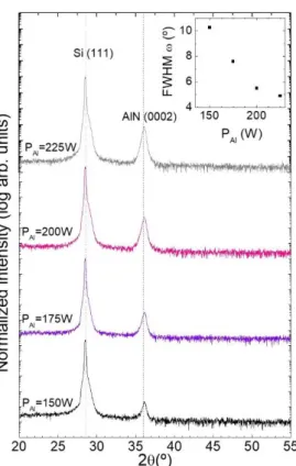
(5) Low temperature photoluminescence (PL) measurements were performed by exciting the samples with 25 mW of a continuous-wave Ar+ laser (λ = 488 nm) focused onto a 50-μm-diameter spot. The PL emission was collected by a 45-cm-focal-length Jobin-Yvon monochromator equipped with a charge-coupled-device camera. The processed samples were characterized by current density-voltage (JV) measurements carried out in the dark and under illumination. The measurements in the dark were recorded with an Agilent 4155C parameter analyzer, whereas the measurements under illumination were performed in a Spectra-Nova's CT Series Solar Cell Tester (Class AAA) solar simulator under simulated AM1.5G spectrum (100 mW/cm2). The spectral response of the devices in the 380-1200 nm range was measured at zero bias using a 250 W halogen lamp coupled to an Oriel Instruments Cornerstone 130 1/8m monochromator. These results are calibrated using the response of the cell to a GaN-based laser diode emitting at 405 nm. The external quantum efficiency (EQE) is estimated from the responsivity with the equation EQE = R ℎ𝑐/𝑞𝜆, where R is the responsivity, q is the electron charge, and hc/λ is the photon energy. 3.. Results and discussion. 3.1. AlN growth conditions optimization. Effect of the power applied to the aluminum target The properties of AlN films grown on Si (111) have been studied as a function of the power applied to the aluminum target (PAl), which was ranged from 150 to 225 W. The substrate temperature (450°C) was chosen to avoid the growth interruption that would be required to change the growth temperature between the AlN buffer and the AlInN layer. For this study, the AlN growth time was fixed to 2 h for all samples. This study extends the range of PAl analyzed in previous reports published by our group concerning the growth of AlN on sapphire substrates [33]. Figure 1 shows the HRXRD 2θ/ω scans of the AlN layers grown with different PAl. All the layers present crystalline wurtzite structure highly oriented along the c-axis. The intensity of the diffraction peak increases with the PAl pointing to an increase in the layer thickness. The strain state along the growth axis (zz), calculated as the relationship between the experimental and theoretical for fully 4.
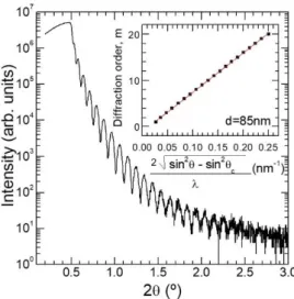
(6) relaxed AlN (4.982 Å) c-lattice parameter, is in the range of −0.31 to −0.21%, decreasing for increasing the power applied to the aluminum target. Therefore, the layers grow under tensile strain, as expected [34].. Figure 1. (Color online) HRXRD scans of the AlN layers grown applying different power to the aluminum target, the dash lines corresponds with the theoretical diffraction angles of relaxed Si(111) and AlN(0002). Inset: FWHM of the (0002) AlN rocking curve as a function of PAl for the AlN layers. The grain size (Gs) is estimated with the Scherrer equation from HRXRD measurements; (𝐺𝑠 =. 0.9𝜆 𝑐𝑜𝑠𝜃) ∆2𝜃. where Δ2θ is the FWHM of the (0002) AlInN reflection in the 2θ/ω scan, θ is the. diffraction angle and λ is the incident X-ray wavelength. An increase in the Gs from 19 to 22 nm is shown when increasing the PAl from 150 and 225 W. The inset in Figure 1 shows the evolution of the FWHM of the rocking curve of the (0002) AlN diffraction peak as a function of the PAl. The increase of the PAl from 150 to 225 W leads to a decrease of the FWHM of the rocking curve from 10 to 4.9°. The layer thickness was obtained from X-ray reflection (XRR) measurements (see the inset of Figure 2), through the spacing between maximums of the reflectivity corrected with the critical angle (θc) 5.
(7) together with the Bragg's equation(2𝑑√𝑠𝑖𝑛2 𝜃 − 𝑠𝑖𝑛2 𝜃𝑐 = 𝑚𝜆), with m being an integer number indicating the diffraction order. The layer thickness for the samples grown with different power applied to the aluminum target increases from 85 nm to 140 nm when increasing the PAl from 150 to 225 W, resulting in a linear increase of the growth rate from 43 nm/h to 72 nm/h. From θc, it is also possible to estimate the AlN density, which increases from 2.66 to 2.91 g/cm3 when increasing the power applied to the aluminum target from 150 to 225 W, i.e. the layers become more compact due to the increased adatom mobility. However, these values are still below the theoretical one of 3.27 g/cm3 [35].. Figure 2. (Color online) XRR scan of the AlN thin film deposited at 150 W. Inset: estimation of the layer thickness. The surface morphology of the samples was assessed by AFM measurements. The images in Figure 3 show that the diameter of the grains increases with PAl, which leads to a decrease of the root-meansquared (RMS) surface roughness. The lowest RMS roughness (0.64 nm) is obtained for the sample grown at 225 W. The smoothness of the layers points out that there is no damage in the surface due to ion bombardment in the range of PAl under study.. 6.
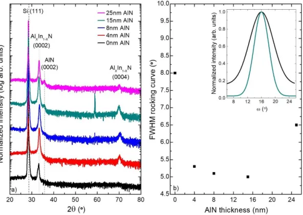
(8) Figure 3. (Color online) a) Variation of the RMS surface roughness as a function of PAl. AFM images of the AlN samples with different PAl b) 150 W, c) 175 W, d) 200 W, e) 225 W. In conclusion, the increase of PAl leads to an enhancement of the grain size, growth rate and density of the AlN film, with a decrease of the RMS surface roughness. Taking into account these results, the power applied to the aluminum target for the growth of AlN as buffer layer for the AlxIn1-xN on Si (111) heterojunctions is 225 W. 3.2. Effect of the AlN thickness on the properties of AlInN films To study the effect of the thickness of the AlN buffer layer on the subsequent growth of AlxIn1-xN, a set of five samples with different AlN thicknesses (dAlN = 0 25 nm) were grown. The AlxIn1-xN layer thickness was fixed to 80 nm in all samples of the series. This thickness was chosen taking into account the potential application of the structures to photovoltaic devices. 3.2.1. Structural and chemical properties Figure 4a) displays the 2θ/ω scans the AlInN films, showing that all layers present crystalline wurtzite structure. The diffraction peaks of the (111) silicon substrate, the (0002) AlN, and the (0002) and (0004) AlInN layers appear in the scan, which show no sign of phase separation. In addition, the enhancement of the peak intensity in samples with AlN buffer layer, which allows resolving the (0004) AlxIn1-xN diffraction peak, confirms the improvement of the crystalline quality, which is also supported by the FWHM of the 2θ/ω (0002) AlInN diffraction peak decreasing monotonically with the 7.
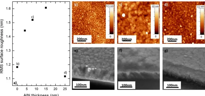
(9) buffer layer thickness, from 0.587° for dAlN = 0 nm to 0.471° for dAlN = 15 nm, and 0.41° for dAlN = 25 nm. Furthermore, the FWHM of the rocking curve of the (0002) reflection of AlInN is also reduced when inserting the AlN layer, as shown in Figure 4b). However, in this case, a degradation is observed for the sample with the thickest buffer layer (dAlN = 25 nm).. Figure 4. (Color online) a) X-ray 2θ/ω scans of the AlxIn1-xN samples grown with different AlN buffer layer thickness. b) Evolution of the FWHM of the rocking curve with the AlN thickness, inset: rocking curve of the samples under study. The morphological features of the layers were assessed by AFM and FESEM measurements. As illustrated in Figure 5, the layers are compact in all cases, with a granular surface morphology. Figure 5a) depicts the evolution of the 1×1 µm2 RMS surface roughness as a function of the AlN buffer layer thickness, showing that in all cases the RMS surface roughness is below 1.7 nm.. 8.
(10) Figure 5. (Color online) a) Progress of the 1×1µm2 RMS surface roughness as a function of the AlN buffer layer thickness. AFM (1×1µm2) and FESEM images of the AlxIn1-xN layer: b), e) without AlN buffer layer; c), f) with 8 nm AlN buffer layer; d), g) with 25 nm AlN buffer layer. Finally, TEM measurements, performed in similar samples grown under the same growth conditions, were carried out in order to visualize the interface between the nitride layer and the silicon substrate. Figure 6 displays TEM images under diffraction contrast conditions of a) the AlInN sample without buffer layer, and b) the sample with 15 nm AlN buffer layer, showing compact AlInN layers with smooth surface, consistent with AFM and FESEM characterization. Figure 6b) shows the homogeneous AlN buffer layer covering the entire substrate surface. Both samples contain structural defects running along the growth direction (see the white arrows in Figure 6), but their density is reduced by one order of magnitude when introducing the AlN buffer layer (from 1011 cm−2 to 1010 cm−2).. 9.
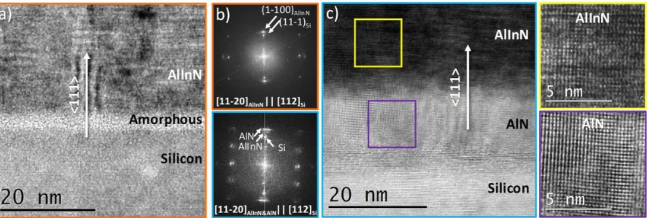
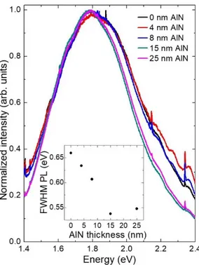
(11) Figure 6. (Color online) TEM images acquired under diffraction contrast conditions of a) a sample without buffer layer; b) a sample with 15 nm AlN buffer layer. White arrows point to structural defects propagating along the growth direction. High-resolution TEM images of the interface are presented in Figure 7a) and c) for AlInN/p-Si and AlInN/AlN/p-Si heterojunctions, respectively. Both, the AlN buffer and the AlInN layer share the crystalline phase, growth direction and orientation, and are grown showing the following epitaxial relationship with the substrate: (0001)[11-20] AlInN and (0001)[11-20] AlN || (11-1)[112] Si. In absence of the AlN buffer layer, there is a 2-3 nm-thick amorphous layer at the interface between the silicon substrate and the AlInN (see Figure 7a)), which is not observed on the sample containing the 15 nm AlN buffer layer (Figure 7c)). A possible explanation is that the Al atoms reaching the silicon surface when growing the AlN buffer have a higher kinetic energy than those reaching the substrate for the growth of AlInN due to the higher power applied to the aluminum target, so that they are able to break the bonds that form the amorphous layer. Additional measurements performed by EELS (not shown here) discard In or Al interdiffusion between phases, evidencing a well-defined interface between the AlN and the AlInN.. Figure 7. (Color online) High resolution TEM analyses a) for the sample without buffer layer and c) for the sample with 15 nm AlN buffer layer, along with their Fast Fourier Transform b) evidencing the epitaxial relationship. 3.2.2. Optical properties The optical properties of the layers were assessed by low temperature (T = 5 K) PL measurements (see Figure 8). The PL energy peak is located around 1.8 eV for all samples, a very similar value to the one obtained for thick (460 nm) AlxIn1-xN on Si(111) layers without buffer and with the same Al mole. 10.
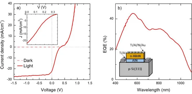
(12) fraction grown under similar growth conditions [20]. The FWHM of the PL decreases when increasing the AlN buffer layer thickness (see inset in Figure 8).. Figure 8. (Color online) Low temperature (T = 5 K) PL measurements of the AlxIn1-xN samples with different AlN thickness. Inset: Evolution of the FWHM of the PL with the AlN buffer layer thickness. 3.3. Characterization of n-AlInN/AlN/p-Si heterojunctions The n-AlInN/AlN/p-Si heterojunctions were processed and contacted to be characterized as solar cells. The size of the devices was delimited with a 1×1 mm2 mesa structure patterned by sputtering etching with Ar. The p-contact was formed by evaporation of Ti/Al (50/100 nm), annealed at 550°C under nitrogen atmosphere. The n-contact consists of a finger pattern of Ti/Al/Ni/Au (30/70/20/100 nm) with 5 µm finger width and a 150 µm pitch. A schematic drawing of the device is included as inset in Figure 9b). Figure 9a) shows the JV curves measured in the dark and under illumination (1 sun AM1.5G) of the n-AlInN/AlN/p-Si (80/4 nm) heterojunction. This device presents series resistance Rs = 90 Ω, shunt resistance Rsh = 30 MΩ, and ideality factor n = 4.5, calculated from the JV characteristic under dark conditions. The high value of the ideality factor can be related with recombination at the interface of the heterojunction or to the required tunneling transport through the AlN buffer layer. 11.
(13) Figure 9. (Color online) Electrical characterization of the 80 nm AlInN/4 nm AlN/p-Si (111) heterojunction, a) JV characteristics in the dark and under illumination (AM1.5G). b) External quantum efficiency. Inset: sketch of the solar cell device. Under illumination, the structure presents open circuit voltage Voc = 0.35 V, short circuit current density Jsc = 22.2 mA/cm2, and fill factor FF = 20%. However, the plateau shown around 0.4 V in the measurement is related to a non-linear photocurrent behavior. This effect has been previously observed in InGaN/GaN devices [36,37] and indicates a reduction of the generated photocurrent due to inefficient carrier collection, which might be explained by a high recombination rate [38], or by the presence of polarization charges [5,37] at the heterointerface. Figure 9b) shows the spectral variation of the EQE for the AlInN/AlN/Si heterojunction. A maximum EQE = 43.6% is obtained at 560 nm, associated to the response of the AlxIn1-xN layer, whereas the cutoff of silicon is shown at ~900 nm. 4.. Conclusions. In this work, AlN layers were grown on p-Si (111) substrates by RF sputtering. Crystalline layers were obtained even at powers applied to the aluminum target close to the maximum allowed one to avoid surface damaging. The best properties for the AlN are achieved for layers grown at 225 W and 450°C, showing a FWHM of the rocking curve of 5°, a density of 2.91g/cm3 and a RMS surface roughness of 0.64 nm. 12.
(14) We have demonstrated that the crystal quality of Al0.37In0.63N layers is improved when using an AlN buffer layer on p-Si (111). All the layers under study are crystalline with wurtzite structure highly oriented in the c-axis regardless the buffer layer thickness. The crystal quality is improved when the AlN buffer layer is in the 4 to 15 nm range achieving a minimum (5°) FWHM of the (0002) AlxIn1-xN rocking curve for layers grown with 15 nm AlN buffer layer. All samples present compact morphology with a RMS surface roughness below 1.7 nm. HRTEM measurements show that the presence of the AlN prevents the formation of an amorphous phase between the silicon substrate and the AlInN layer. Low temperature PL emission at 1.8 eV is obtained for all AlInN/AlN/Si structures. The 80 nm n-AlInN/4 nm AlN/p-Si heterojunction has been processed into a solar cell device. The extracted values from the JV characteristics in the dark and under illumination evidence the low and high series (Rs = 90 Ω) and shunt resistances (Rsh = 30 MΩ), respectively, with Jsc = 22.2 mA/cm2 and Voc = 0.35 V. The EQE covers the visible spectral range with a maximum of 43.6% at 560 nm. The device operation of AlInN as alternative electron-selective contact in Si heterojunction solar cells can be amended by reducing the Si contact resistivity and passivating the Si surface to decrease the interface recombination.. Acknowledgements We thank L. Grenet from the CEA-Grenoble (LITEN) and University Grenoble Alpes, France, for the JV characteristics performed under AM1.5G illumination. Partial financial support provided by: the Spanish Government projects: TEC2014-60483-R, TEC2015-71127-C2-2-R; by the Community of Madrid project: S2013/MIT 2790; by the University of Alcalá project: CCG2015/EXP-014; and by the FPI Grant from the University of Alcalá. Support from Junta de Andalucía (Group INNANOMAT, ref. TEP-946) is also acknowledged.. References [1] 13. I. Saidi, H. Mejri, M. Baira, H. Maaref, Electronic and transport properties of AlInN/AlN/GaN high electron mobility transistors, Superlattices Microstruct. 84 (2015) 113–125..
(15) doi:10.1016/j.spmi.2015.04.036. [2]. C. Berger, A. Dadgar, J. Bläsing, A. Lesnik, P. Veit, G. Schmidt, T. Hempel, J. Christen, A. Krost, A. Strittmatter, Growth of AlInN/GaN distributed Bragg reflectors with improved interface quality, J. Cryst. Growth. 414 (2015) 105–109. doi:10.1016/j.jcrysgro.2014.09.008.. [3]. A. Yamamoto, M.R. Islam, T.T. Kang, A. Hashimoto, Recent advances in InN-based solar cells: Status and challenges in InGaN and InAlN solar cells, Phys. Status Solidi. 7 (2010) 1309–1316. doi:10.1002/pssc.200983106.. [4]. H.F. Liu, C.C. Tan, G.K. Dalapati, D.Z. Chi, Magnetron-sputter deposition of high-indiumcontent n-AlInN thin film on p-Si(001) substrate for photovoltaic applications, J. Appl. Phys. 112 (2012) 63114. doi:10.1063/1.4754319.. [5]. H.F. Liu, S.B. Dolmanan, S. Tripathy, G.K. Dalapati, C.C. Tan, D.Z. Chi, Effects of AlN thickness on structural and transport properties of In-rich n-AlInN/AlN/p-Si(0 0 1) heterojunctions grown by magnetron sputtering, J. Phys. D. Appl. Phys. 46 (2013) 95106. doi:10.1088/0022-3727/46/9/095106.. [6]. J. Wu, W. Walukiewicz, K.M. Yu, J.W. Ager, E.E. Haller, H. Lu, W.J. Schaff, Y. Saito, Y. Nanishi, Unusual properties of the fundamental band gap of InN, Appl. Phys. Lett. 80 (2002) 3967–3969. doi:10.1063/1.1482786.. [7]. W.M. Yim, E.J. Stofko, P.J. Zanzucchi, J.I. Pankove, M. Ettenberg, S.L. Gilbert, Epitaxially grown AlN and its optical band gap, J. Appl. Phys. 44 (1973) 292–296. doi:10.1063/1.1661876.. [8]. O. Ambacher, Growth and applications of Group III-nitrides, J. Phys. D. Appl. Phys. 31 (1998) 2653–2710. doi:10.1088/0022-3727/31/20/001.. [9]. H. Kim-Chauveau, P. de Mierry, J.-M. Chauveau, J.-Y. Duboz, The influence of various MOCVD parameters on the growth of Al1−xInxN ternary alloy on GaN templates, J. Cryst. Growth. 316 (2011) 30–36. doi:10.1016/j.jcrysgro.2010.12.040.. [10]. D.A. Neumayer, J.G. Ekerdt, Growth of Group III Nitrides. A Review of Precursors and Techniques, Chem. Mater. 8 (1996) 9–25. doi:10.1021/cm950108r.. [11]. C. Hums, J. Bläsing, A. Dadgar, A. Diez, T. Hempel, J. Christen, A. Krost, K. Lorenz, E. Alves, Metal-organic vapor phase epitaxy and properties of AlInN in the whole compositional range, Appl. Phys. Lett. 90 (2007) 22105. doi:10.1063/1.2424649.. [12]. M. Ferhat, F. Bechstedt, First-principles calculations of gap bowing in InxGa1-xN and InxAl1xN alloys: Relation to structural and thermodynamic properties, Phys. Rev. B. 65 (2002) 75213. doi:10.1103/PhysRevB.65.075213.. [13]. A. V. Lobanova, E. V. Yakovlev, R.A. Talalaev, S.B. Thapa, F. Scholz, Growth conditions and surface morphology of AlN MOVPE, J. Cryst. Growth. 310 (2008) 4935–4938. doi:10.1016/j.jcrysgro.2008.07.098.. [14]. Y. Taniyasu, M. Kasu, T. Makimoto, Threading dislocations in heteroepitaxial AlN layer grown by MOVPE on SiC (0001) substrate, J. Cryst. Growth. 298 (2007) 310–315. doi:10.1016/j.jcrysgro.2006.10.032.. [15]. J. Kamimura, T. Kouno, S. Ishizawa, A. Kikuchi, K. Kishino, Growth of high-In-content InAlN nanocolumns on Si (1 1 1) by RF-plasma-assisted molecular-beam epitaxy, J. Cryst. Growth. 300 (2007) 160–163. doi:10.1016/j.jcrysgro.2006.11.029.. [16]. W. Chen, Y. Wu, J. Tian, T. Yen, P. Lin, J. Chen, C. Hsiao, L. Chang, Effect of Growth Temperature on Structural Quality of In-Rich InxAl1-xN Alloys on Si ( 111 ) Substrate by RFMOMBE, ISRN Nanomater. 2014 (2014).. [17]. S. Karmann, H.P.. Schenk, U. Kaiser, a Fissel, W. Richter, Growth of columnar aluminum nitride layers on Si(111) by molecular beam epitaxy, Mater. Sci. Eng. B. 50 (1997) 228–232. doi:10.1016/S0921-5107(97)00168-2.. [18]. G. Koblmueller, R. Averbeck, L. Geelhaar, H. Riechert, W. Hösler, P. Pongratz, Growth diagram. 14.
(16) and morphologies of AlN thin films grown by molecular beam epitaxy, J. Appl. Phys. 93 (2003) 9591–9596. doi:10.1063/1.1575929. [19]. N. Afzal, M. Devarajan, K. Ibrahim, Influence of substrate temperature on the growth and properties of reactively sputtered In-rich InAlN films, J. Mater. Sci. Mater. Electron. 27 (2016) 4281–4289. doi:10.1007/s10854-016-4294-y.. [20]. A. Núñez-Cascajero, L. Monteagudo-Lerma, S. Valdueza-Felip, C. Navío, E. Monroy, M. González-Herráez, F.B. Naranjo, Study of high In-content AlInN deposition on p-Si(111) by RFsputtering, Jpn. J. Appl. Phys. (2016). doi:10.7567/JJAP.55.05FB07.. [21]. J.X. Zhang, H. Cheng, Y.Z. Chen, A. Uddin, S. Yuan, S.J. Geng, S. Zhang, Growth of AlN films on Si (100) and Si (111) substrates by reactive magnetron sputtering, Surf. Coatings Technol. 198 (2005) 68–73. doi:10.1016/j.surfcoat.2004.10.075.. [22]. J.H. Yang, S.M. Kang, D. V. Dinh, D.H. Yoon, Influence of AlN buffer layer thickness and deposition methods on GaN epitaxial growth, Thin Solid Films. 517 (2009) 5057–5060. doi:10.1016/j.tsf.2009.03.089.. [23]. W. Luo, X. Wang, L. Guo, H. Xiao, C. Wang, J. Ran, J. Li, J. Li, Influence of AlN buffer layer thickness on the properties of GaN epilayer on Si(1 1 1) by MOCVD, Microelectronics J. 39 (2008) 1710–1713. doi:10.1016/j.mejo.2008.01.042.. [24]. C.H. Yen, W.C. Lai, Y.Y. Yang, C.K. Wang, T.K. Ko, S.J. Hon, S.J. Chang, GaN-based lightemitting diode with sputtered AlN nucleation layer, IEEE Photonics Technol. Lett. 24 (2012) 294–296. doi:10.1109/LPT.2011.2177654.. [25]. T. Fujimori, H. Imai, A. Wakahara, H. Okada, A. Yoshida, T. Shibata, M. Tanaka, Growth and characterization of AlInN on AlN template, J. Cryst. Growth. 272 (2004) 381–385. doi:10.1016/j.jcrysgro.2004.08.077.. [26]. T.-S. Yeh, J.-M. Wu, W.-H. Lan, The effect of AlN buffer layer on properties of AlxIn1−xN films on glass substrates, Thin Solid Films. 517 (2009) 3204–3207. doi:10.1016/j.tsf.2008.10.101.. [27]. S. Yamaguchi, M. Kariya, S. Nitta, T. Takeuchi, C. Wetzel, H. Amano, I. Akasaki, Anomalous features in the optical properties of Al1−xInxN on GaN grown by metal organic vapor phase epitaxy, Appl. Phys. Lett. 76 (2000) 876–878. doi:http://dx.doi.org/10.1063/1.125615.. [28]. W. Terashima, S.B. Che, Y. Ishitani, A. Yoshikawa, Growth and characterization of AlInN ternary alloys in whole composition range and fabrication of InN/AlInN multiple quantum wells by RF molecular beam epitaxy, Jpn. J. Appl. Phys. 45 (2006) L539–L542. doi:10.1143/JJAP.45.L539.. [29]. S.L. Sahonta, G.P. Dimitrakopulos, T. Kehagias, J. Kioseoglou, A. Adikimenakis, E. Iliopoulos, A. Georgakilas, H. Kirmse, W. Neumann, P. Komninou, Mechanism of compositional modulations in epitaxial InAlN films grown by molecular beam epitaxy, Appl. Phys. Lett. 95 (2009). doi:10.1063/1.3184593.. [30]. K.J. Lesker Company, Practical Process Tips - Sputtering, Lesker Tech. 7 (2010) 1–4.. [31]. A. Núñez-Cascajero, S. Valdueza-Felip, L. Monteagudo-Lerma, E. Monroy, E. Taylor-Shaw, R.W.R. Martin, M. González-Herráez, F.B. Naranjo, E. Taylor, R.W.R. Martin, M. GonzalezHerraez, F. Vega, In-rich Al x In 1 ˗ x N grown by RF-sputtering on sapphire : from closelypacked columnar to high-surface quality compact layers, J. Phys. D. Appl. Phys. 50 (2016) 1–9. doi:10.1088/1361-6463/aa53d5.. [32]. I. Horcas, R. Fernández, J.M. Gómez-Rodríguez, J. Colchero, J. Gómez-Herrero, a. M. Baro, WSXM: A software for scanning probe microscopy and a tool for nanotechnology, Rev. Sci. Instrum. 78 (2007) 13705. doi:10.1063/1.2432410.. [33]. L. Monteagudo-Lerma, S. Valdueza-Felip, A. Núñez-Cascajero, M. González-Herráez, E. Monroy, F.B.B. Naranjo, Two-step method for the deposition of AlN by radio frequency sputtering, Thin Solid Films. 545 (2013) 149–153. doi:10.1016/j.tsf.2013.07.062.. 15.
(17) [34]. D.G. Zhao, S.J. Xu, M.H. Xie, S.Y. Tong, H. Yang, Stress and its effect on optical properties of GaN epilayers grown on Si(111), 6H-SiC(0001), and c-plane sapphire, Appl. Phys. Lett. 83 (2003) 677–679. doi:10.1063/1.1592306.. [35]. T.P. Drüsedau, J. Bläsing, Optical and structural properties of highly c-axis oriented aluminum nitride prepared by sputter-deposition in pure nitrogen, Thin Solid Films. 377–378 (2000) 27– 31. doi:10.1016/S0040-6090(00)01380-8.. [36]. O. Jani, I. Ferguson, C. Honsberg, S. Kurtz, Design and characterization of GaNInGaN solar cells, Appl. Phys. Lett. 91 (2007) 13–16. doi:10.1063/1.2793180.. [37]. C.J. Neufeld, S.C. Cruz, R.M. Farrell, M. Iza, J.R. Lang, S. Keller, S. Nakamura, S.P. Denbaars, J.S. Speck, U.K. Mishra, Effect of doping and polarization on carrier collection in InGaN quantum well solar cells, Appl. Phys. Lett. 98 (2011) 243507. doi:10.1063/1.3595487.. [38]. U. Das, S. Hegedus, L. Zhang, J. Appel, J. Rand, R. Birkmire, Investigation of hetero-interface and junction properties in silicon heterojunction solar cells, 35th Photovolt. Spec. Conf. (2010) 001358–001362. doi:10.1109/PVSC.2010.5614372.. 16.
(18)
Figure
+4
Documento similar
Our results here also indicate that the orders of integration are higher than 1 but smaller than 2 and thus, the standard approach of taking first differences does not lead to
We seek to characterize the transport in a time-dependent flow by identifying coherent structures in phase space, in particular, hyperbolic points and the associated unstable and
Penelitian ini bertujuan untuk mendapatkan asal daerah bahan baku yang terbaik untuk pembuatan sirup gula kelapa dan untuk mendapatkan konsentrasi arang aktif yang
Abstract: Transepidermal water-loss (TEWL), stratum-corneum hydration (SCH), erythema, elas- ticity, pH and melanin, are parameters of the epidermal barrier function and
No obstante, como esta enfermedad afecta a cada persona de manera diferente, no todas las opciones de cuidado y tratamiento pueden ser apropiadas para cada individuo.. La forma
Díaz Soto has raised the point about banning religious garb in the ―public space.‖ He states, ―for example, in most Spanish public Universities, there is a Catholic chapel
teriza por dos factores, que vienen a determinar la especial responsabilidad que incumbe al Tribunal de Justicia en esta materia: de un lado, la inexistencia, en el
Lundvall and Juran's (1974) theory presents a static point of view, insofar as it does not take into account the effects that prevention and appraisal expenditure has on total
