Fuzzy Logic Controllers on Chip
Nelson Acosta & Daniel Simonelli
Universidad Nacional del Centro de la Provincia de Buenos Aires
Departamento de Computación y Sistemas
INCA / INTIA, Tandil, Argentina
Email: nacosta@exa.unicen.edu.ar
www.exa.unicen.edu.ar/inca
Abstract
This paper analyzes a fuzzy logic (FL) oriented instruction set (micro)controller and their implemen-tations on FIPSOC1. VHDL code is synthesized using a small portion of FIPSOC FPGA2. This circuits are used from the mP8051 FIPSOC built-in microcontroller to provide efficient arithmetic operations such as multipliers, dividers, minimums and maximums.
1. Introduction
Fuzzy logic controllers (FLC) can be implemented by software running on standard hardware or on a dedicated microcontroller [Tog86, Wat90, Sas93, Ung93]. Controllers for high rates can be implemented by specific circuits or IC3 [Hun95, Cos96, Aco97, Son00]. In order to process a high number of rules, optimization techniques must be applied; for example: a) reduction of the number of inference computing steps [Des96]; b) parallel inference execution [Aco00, Kov00, Mor00]; c) active rules processing [Aco98, Kas99, Pir01]; and d) standard microcontroller core with a dedicated FL instruction set [Wat93, Wat96].
The digital system speed is limited by maximum total capacitive load of the I/O signals between the different cards and chip packages. Some systems manufacturers have developed a (multi)chip in a package. This approach is also limited by the I/O interface between the different IC in the same package. Other approach proposes to build all system in only one chip. Working inside a SOC the I/O IC system do not affect (greatly) the system performance. The I/O signals between the FPD4 and the mP8051 are connections into the same IC. Systems on a Chip (SOCs) allow to easily prototype mixed signal problems through both hardware capabilities and CAE
software tools. FIPSOC includes a mixed signal programmable device with on-board microprocessor (the FIPSOC chip), a complete set of CAE software tools to manage it, and a set of library macros.
1 FIPSOC: Field Programmable System On Chip. 2 FPGA: Field Programmable Gate Array. 3 IC: Integrated Circuit.
4 FPD: Field Programmable Device (a FPGA like device).
This paper aims to present an alternative scheme to compute the mP8051 controller functions by using a FL instruction set on the FPGA area. Main features of this approach are: a) to reduce the development time by using a well known controller architecture; b) to minimize the algorithm computing time getting faster arithmetic operations.
This paper continues the above research lines by exploring a standard microcontroller core with a dedicated FL instruction set in a SOC5 platform. Some topological and architectural alternatives are analyzed. FIPSOC FPGAs series (provided by SIDSA6) have been utilized as a technological framework. In section II, the main characteristics of the FLC algorithm are summarized. Section III shows some FIPSOC architecture features. Section IV presents an implementation analysis by the arithmetic and lattice units. The architecture are depicted in section V. Finally, the principal results are presented.
2. FLC: The Control Algorithm
An algorithm to compute the m functions f0, f1, ..., fm-1 of n variables x
0, x1, ..., xn-1 is depicted. The value of xi
belongs to a set S
i, and the value of fk to the set of the real
numbers R. To each variable xi correspond pi
membership functions: A
ij: Si
→
[0,1], 0≤
j≤
pi-1; toeach function fk correspond qk decoding functions: Bkl:
[0,1]
→
R, 0≤
l≤
qk-1; the computation of fk is basedon sentences (inference rules) such as: “IF x0 is A0 j0 AND x1
is A1 j1 AND ... AND xn-1 is An-1 jn-1 THEN fk is Bkl”. A
set of coefficients r is defined: r(j0, j1, ..., jn-1, k, l) =1 if
the previously mentioned rule applies; else r(j0, j1, ..., jn-1, k, l) = 0.
The computing algorithm of the fk functions is: ∀i:0 ≤i≤n-1, ∀j:0 ≤j≤pi-1, compute
yij = Aij (xi);
∀k:0 ≤k≤m-1, ∀l:0 ≤l≤qk-1, compute wkl = ∨r (j0, j1, ..., jn-1, k, l) .
y0 j0 . y1 j1 ...
yn-1 jn--1, ∀j0, j1, ..., jn-1
vkl = Bkl (wkl); ∀k:0 ≤k≤m-1, compute
Nk = vk 0 + vk 1 + ... + vk qk-1, Dk = wk 0 + wk 1 + ... + wk qk-1,
fk = Nk / Dk
This scheme needs to compute all the lattice (maximum, minimum) and arithmetic (add, multiplication, division) operations. The inference mechanism uses the lattice max-min operations to evaluate the fuzzy-rule set. The multiplication and division instructions are used during the defuzzification step and sometimes to compute the membership functions. This scheme uses a set of LUT to compute the membership functions (during the fuzzification and defuzzification).
This scheme needs the reduction of the lattice and arithmetic expressions to two-operand equivalent ones. This reduction is based on the properties of the domain space. It does not use the knowledge of fuzzy inference mechanisms.
3. FIPSOC Architecture Topics
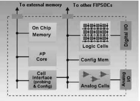
This prototyping and integration system, consists of a mixed-signal Field Programmable Device (FPD) with a standard mP8051 core, a suitable core of CAD tools and a set of library macros and cells which support a number of typical applications to be easily mapped onto the FPD. A set of fixed-functionality yet configurable analog cells is also provided [Bae97, Fau97].
The FIPSOC chip includes a two-dimensional array of programmable DMCs (Digital Macro Cell). The DMC is a large granularity, Look Up Table (LUT) based, synthesis targeted 4-bit wide programmable cell.
Each DMC has two main blocks: a combinational part, composed of four 4-input LUTs, and a sequential block including four FFs. Any lookup table (LUT) can
implement any input Boolean function. Every two 4-input LUTs share two 4-inputs, and two LUTs can be combined to form a 5 input function or a 4 to 1 multiplexer (four inputs and two control bits). The four LUTs of a DMC can be combined to perform any 6-input Boolean function. (Figure 1)
The sequential part of the DMC includes four two-input flip-flops (FF), each of which can be independently configured as mux-type or enable-type, as latch or FF, and with synchronous and asynchronous set or reset.
[image:2.595.311.546.294.463.2]To improve chip area, the number of shared segments in a point to point net should be maximized, as this consume less FPGA routing resources. This tradeoff forces the design of complex routing channels, with different length segments, which requires sophisticated Computer Aided Design (CAD).
Figure 1 – FIPSOC Block Diagram
3.1. 8051 Memory Organization
The memory map of the on-chip mP8051 keeps; by default, the memory organization of the original 8051. That is, it has a separate address space for Program Memory and Data Memory, distributed in the following four addresses spaces:
• Up to 64 Kbytes of Program Memory,
• Up to 64 Kbytes of external Data Memory,
• 256 bytes of internal Data Memory,
• 128 bytes of Special Function Registers area.
• 64 bytes of internal data memory, called buffer access area,
• Up to 16 Kbytes memory mapped on the lower external Data Memory (depending on device)
3.1.1. Program Memory.
The Program Memory of the on-chip mP8051 consists an internal and an external space. 512 bytes of Program Memory resides on-chip (dedicated to the FIPSOC boot program).
3.1.2. General Purpose Registers
The lower 32 positions of the internal RAM are grouped into four banks of 8 registers. Only one of the banks may be enabled at a time (two bits of PSW register are used to select the active bank). For indirect addressing, two of them are used as pointer or index registers.
3.1.3. Special Function Registers (SFR)
The SFR area is located in the upper 128 bytes of the internal memory. It has two important functions: Firstly, all CPU registers reside in this area (excepting PC and GPR banks). Secondly, a number of registers (not included in the SFR area of the original 8051) constitute the interface between the mP8051 and all the on-chip subsystems.
SFR, which are located in addresses which are multiple of eight, are both byte- and bit-addressable. All SFR can be accessed by direct addressing only.
Note that not all of the addresses are occupied. Unoccupied addresses are not implemented on the chip (and the may be used in future). Read access to these addresses will return random data; write accesses will be ignored.
3.2. Subsystems Interface
The configuration and control of the subsystems that are included in the FIPSOC chip are realized through accesses to locations of the different memories of the mP8051. Some memory locations of the SFR area have been reserved for system configuration and general- purpose control.
The subsystems and the memory used for configuration are listed below:
a) The programmable blocks (CAB and PL block) are configured (and accessed) using special function registers and data memory (both internal and external) of the mP8051 memory organization. Thus, the configuration and data transfer of these blocks is made through positions located in both internal and external memories.
• Programmable Logic Block: Either internal or external memory locations may be used to configure, control and transfer data. In particular, both configuration memory and hardware outputs of the DMC are mapped in both internal (buffer access) and external; LUT memory data in DMCs can be accessed through internal memory only.
• Configurable Analog Block (CAB): The configuration of the block is made through the buffer access area only; Data transfer is made using memory locations of the SFR area.
b) Other subsystems are configured and controlled with special function registers only. These blocks are the Clock Generation Block (CGB), Interrupt Service Block, Serial Communication Block, Debugger Block, Watchdog Block and other mP8051 peripherals systems (Parallel & Serial I/O, Timers, etc.)
Configuration memories and outputs of the programmable blocks (PL and CAB) may be accessed through internal and external memory locations.
3.3. PL Subsystem Interface
Regular Configuration Memory: This memory may be mapped either through internal memory (data buffer access) or external memory. If a buffer access is done, row and column mask registers are needed, with the purpose of selecting the desired DMC(s), IO cell(s) or IIC (Internal Interface Cell) routing resources cell(s).
3.4. Extended SFR map
The new special function registers added to the original SFR map of the 8051 are dedicated to control, configure and data transfer purpose. Only 18 of them are related to the programmable blocks interface and the system mapping control.
3.5. Port Access
Figure 2 – Fast access bus interface
4. Instruction Analysis
Multiplication is always an essential function in digital systems. This work is focused on parallel multipliers which are oriented to increase the mP8051 processing speed in a FL application.
Here are depicted the seven multipliers organized depending on the way they communicate their EPs (elementary processors) [Col99]. Every multiplier calculates A*B+C+S, generating a resulting number sized as length(A) plus length(B). The seven multipliers let to use different topologies and architectures.
• With Local Communication. McCanny - McWhirter. De Mori.
• With Global Communication. Hatamian & Cash. Ripple – Carry. Carry Save.
• With Mixed Communication. Guild.
De Mori – Guild.
The goal was to analyze FPGA occupation factors. With that idea in mind, 2-bit, 3-bit and 4-bit wide multipliers were used, fully combinational and with pipeline granularity 1. Although it may seems that these are very restrictive sizes, main idea is to use them for implementing iterative multipliers where, for example, an 8 x 8 multiplication can be obtained through 4 operations with a 4 x 4 multiplier.
The lattice operations involve a reduced arithmetical unit that computes the maximum and minimum values. Each of this units includes a set of registers to be used as local
RAM. The mP8051 saves the values in between the maximum or minimum must be computed. The unit output is registered too. This working scheme free the microcontroller to do any other operations while the computing is done.
For materializing these circuit structural RTL7 VHDL8 code was generated [BJM93, Boe96, Bue98, Col99] to configure the built-in FIPSOC FPGA [Fau97].
Other architectural option works by using a hardwired stack. The mP8051 push the two operands and the operator in the stack. The operator value activates the circuit starting to compute. When the unit finished the required operation, it pushes the resulting into the stack to be acquired by the mP8051.
The operations (maximum, minimum, multiplication and division) are implemented full combinational in this version; while the lattice operations are computed by a unit. The architecture design uses an 8-bit main bus joining the mP8051 I/O port to each computing unit. The right unit selection is done by a 2-bits selector:
0000 Write 1st Op Multiplication 0001 Write 2nd Op Multiplication 0010 Read Low Byte Multiplication 0011 Read High Byte Multiplication 0100 Write 1st Op Division
0101 Write 2nd Op Division 0110 Read Integer Division 0111 Read Remainder Division 1000 Unused
1001 Write 1st Op Maximum 1010 Write 2nd Op Maximum 1011 Read Resulting Maximum 1100 Unused
1101 Write 1st Op Minimum 1110 Write 2nd Op Minimum 1111 Read Resulting Minimum
The computing units let the programmer the responsibility to take into account the resulting value stability. This feature lets to save: (a) some mP8051 I/O port bits, and (b) computing time of a polling operation to check if the unit have finished.
5. Architecture analysis
Parameters considered after 42 implementations were: minimum required LUT size, number of DMCs and FFs used. From routing resources point of view, congestion
7 RTL: Register Transfer Level.
and used-shared segments were taken into account. These quantities, give useful information about detailed routing algorithm, RAISE (Router using Adaptive Simulated Evolution) [Bae97] which yields an idea regarding efficient use of routing resources through the maximization of shared segments.
A crucial restriction is to provide FIPSOC with cheap FL core (in terms of programmable resources), therefore is very important to handle this information for not wasting too much of the interconnection resources.
6. Conclusions
Dedicated fast FL operations greatly increases the FLC system efficiency and performance. This feature let users to use parallelism between the mP8051 code, the lattice and the arithmetic operations. It also opens the door to many applications involving this kind of computation, where the previous standard microcontrollers were not fast enough or too inefficient. It would be necessary to develop a software to verify the possible timing violations.
Independently of the multiplier used, with a 3-bit input and no pipeline, the placement tool assigns a 5-bit LUT, as well as a low FFs usage from DMCs. As a matter of fact, except on the De Mori - Guild multiplier, FFs usage factor is less than 50%. Particularly, for Ripple - Carry multiplier, using pipeline with granularity 1 only implies adding one single DMC. Moreover, it improves FFs usage as well as diminish LUTs size.
A general consequence of this fact is that, regardless data size, in all those cases on which the combinational version had 5-bit LUTs, passing to a version with pipeline yielded a DMCs increment that never arrived to duplicate the original value, as long as in that cases with 4-bit LUTs, adding pipeline resulted on two times or even more DMCs.
This is a very relevant fact at the time of choosing a combinational scheme to save programmable resources: here is shown that depending on the situation, it is possible to obtain a pipelined scheme with a low impact additional cost.
As a future work, it is necessary to obtain the power consumption related to each FLC. An equation must describe area and speed behavior. This approach let the designer to estimate these metrics before the place and route. The parallel inference by using multiples max-min computing units is a key to try.
References
[Aco00] Acosta N. & Curti H. “Motores de Inferencia para Controladores Difusos: análisis de materializaciones hardware”. ICIE, UBA, Bs. As. 26-28 abril 2000.
[Aco97] Acosta N., Deschamps J-P. and Sutter G. “Automatic Program Generator for Customized Fuzzy Logic Controllers”. Proc. IFAC AART´97, Vilamoura, Portugal, April 1997, pp: 259-265.
[Aco98] N. Acosta, J-P Deschamps y J. Garrido. “Optimized active rule fuzzy logic custom controller”, Int. Symposium EIS'98, Tennerife, España. Feb'98.
[Bae97] V. Baena-Lecuyer, M. A. Aguirre, A. Torralba, L.G. Franquelo & J. Faura, “RAISE: A Detailed Routing Algorithm for Field-Programmable Gate Arrays”, DCIS'97 [BJM93] E.I. Boemo, E. Juárez y J. Meneses;
“Taxonomía de Multiplicadores”; VIII DCIS Conference, Universidad de Málaga, Noviembre de 1993.
[Boe96] E. Boemo; "Contribution to the Design of Fine-Grain Pipelined Arrays";
http://www.ii.uam.es/~ivan/; Jan 1996. [Bue98] S. López Buedo; "The Webgen Project";
http://www.ii.uam.es/~eda; 1998. [Col99] C. Collado & K. Larsen; "Sistema de
Asistencia en el Diseño de Multiplicadores"; UNCPBA, Fac. Ciencias Exactas, Tandil, 1999.
[Cos96] Costa A., De Gloria A. and Olivieri M. “Hardware design of Asynchronous Fuzzy Controllers”. IEEE Trans. on Fuzzy Systems, vol. 4, Nro. 3, Aug. 1996, pp.: 328-338. [Des96] Deschamps J-P and Acosta N. “Algoritmo de
optimización de funciones reticulares aplicado al diseño de Controladores Difusos”. 25as. JAIIO, 1996 pp: 1.17-1.27.
[Fau97] Julio Faura, Miguel A. Aguirre, Juan M. Moreno, Phuoc van Duong, Josep M. Insenser, "FIPSOC: A Field Programma-ble System On a Chip", DCIS'97
[Hun95] Hung D. L. (1995). “Dedicated Digital Fuzzy Hardware”. IEEE Micro, vol. 15, nro. 4, pp: 31-39.
[Kov00] Z. Kovacic, S. Bogdan & T. Reichenbach. “NonLinear Position Control By Using Multiple Position-Dependent Self-Organizing Fuzzy Logic Controllers”, 6th IFAC-Symposium on Robot Control SYROCO ´00, pp.229-233 , Vienna, Austria, 2000..
[Mor00] Hipolito Moreno Llagostera. “Control of a Pneumatic Servosystem using Fuzzy Logic”, 1st. FPNI - PhD Symposium. Hamburg, 2000. Pp. 189-201.
[Pir01] Leonardo Pirrello, Leena Yliniemi & Kauko Leiviskä. “Development of a Fuzzy Logic Controller for a Rotary Dryer with Seft-Tuning of Scaling Factor”, Oulu University, Control Eng. Laboratory, Report A17, Oulu, Finland. ISBN 951-42-6424-X. June 2001. [Sas93] Sasaki M. Ueno F. and Inoue T. (1993). “7.5
MFLIPS Fuzzy Microprocessor using SIMD and Logic-in-Memory Structure”. Proc. of IEEE International Conference on Fuzzy Systems, pp: 527-534.
[Son00] Feijun Song & Samuel M. Smith. “ Takagi-Sugeno Type Fuzzy logic Controller with only 3 RUles for a 4 Dimensional Inverted Pendulum System”, IEEE Int. Conf. System, Man & Cybernetics, pp.3800-3805, 2000.
[Tog86] Togai M. and Watanabe H. (1986). “Expert System on a Chip: An Engine for Real-Time Approximate Reasoning”. IEEE Expert, vol. 1, Nro. 3, pp: 55-62.
[Ung93] Ungering A., Thuener K. and Gosser K. (1993). “Architecture of a PDM VLSI Fuzzy Logic Controller with Pipelining and Optimized Chip Area”. Proc. of IEEE International Conference on Fuzzy Systems, pp: 447-452.
[Wat90] Watanabe H, Dettlof W. and Yount K. (1990). “A VLSI Fuzzy Logic Controller with
Reconfigurable, Cascadable Architecture”. IEEE Journal on Solid-State Circuits, vol. 25, nro. 2.
[Wat93] H. Watanabe y D. Chen. “Evaluation of fuzzy instructions in a RISC processor”, Proc. IEEE Int. Conf on Fuzzy Systems, San Francisco, pp: 521-526, 1993.
[Wat96] H. Watanabe, D. Chan y S. Konuri.