IV Nanowires: A Study of the Electromagnetic Field
Enhancement in Homogeneous and Heterostructured
Nanowires
Jose Luis Pura, Julián Anaya, and Juan Jim
'
enez*
1. Introduction
Semiconductor nanowires (NWs) attract the attention of the scientific community because of the increasing number of applications based on their unique properties.[1] These
J. L. Pura, J. Anaya[+], Prof. J. Jim'enez
GdS Optronlab
Física de la Materia Condensada Ed. Lucia
Univ. de Valladolid
Paseo de Bel'en 19, 47011 Valladolid, Spain
E-mail: [email protected]
The ORCID identification number(s) for the author(s) of this article can be found under https://doi.org/10.1002/pssa.201800336.
[þ]Present address: MTC – Manufacturing Technology Centre, Ansty
Park, Coventry CV79JU, UK
DOI: 10.1002/pssa.201800336
properties arise from the confined di- mension, the diameter, as compared to some characteristic lengths. Among other, the radius of the Bohr exciton for quantum confinement, the phonon mean free path for thermal conductivity, or the wavelength of the incident electromag-
netic (EM) waves for optical antenna effects.[1] There is a great interest about the interaction between semiconductor NWs and light, because the optical properties of the NWs make of them the optimal candidates for the future nanophotonic devices. Several unique optical properties of semiconductor NWs have been reported lately, for example, waveguiding,[2] optical resonan- ces,[3] antenna effects,[4] etc. These effects are modulated by the NW diameter, the laser wavelength, and the dielectric properties of the NW and its surrounding medium. For certain NW diameters, resonant optical absorption/scattering takes place, resulting in large local EM fields inside the NW,[5,6] which can be experimentally investigated by microRa- man spectroscopy.[3,7–9]
Up until now, most of the research effort has been focused on homogeneous NWs; however, heterostructured NWs are neces- sary for the fabrication of advanced devices. Some effort has been focused on core/shell heterostructured NWs, mainly focused on the stress assessment,[10,11] but much less effort has been
devoted to the optical properties of axially heterostructured NWs. In previous papers, we demonstrated the need of studying individual NWs,[12] mainly because of the optical response of bundles of NWs is disturbed by the very different NWs dimensions probed by the laser beam, as well as by their spatial distribution withinthelaser beam spot. The mainissue withthis approach, that is, usingindividual NWs, is thatthe Ramansignalwouldbenotably weak. Individual NWs have a very small scattering volume as compared to a bulk sample; therefore, one could expect a very low Ramansignal arising from them. Fortunately, as we will show later on, the unique properties of the NWs come to help us and the Raman signal of an individual NW can be almost equivalent to the Ramansignalarisingfrom the corresponding bulk semiconductor under the same experimental conditions.
�
8 -2
The interaction between a NW and light can be analyzed in the frame of the Lorenz–Mie theory,[13] or more accurately by solving the full Maxwell equations for this interaction. Here we have solved the EM equations by finite element methods (FEMs) for different NW configurations, that is, homogeneous group IV NWs, core/shell SiGe/Ge NWs, and axially heterostructured SiGe/Si NWs and the results are compared to the experimental micro-Raman results.
2. Experimental Section
We have studied the light/NW interaction in group IV semiconductor NWs, both homogeneous Si NWs, and axially heterostructured SiGe/Si NWs, grown by the vapor-liquid-solid (VLS) method, using Si2H6 and GeH4 as precursor gases and Au
metal droplets as the catalysts. VLS growth is the most extended method to grow bottom up NWs; however, it does not provide abrupt axial SiGe/Si heterojunctions, because of the high solubility of group IV semiconductors in Au. Once the gas sources are switched-off to change the NW composition, the reservoir effect, due to the remaining atoms solved in the catalysts droplet, avoids the formation of sharp interfaces.[14,15] The heterojunction appears as a region of graded composition from the nominal Ge concentration of the SiGe segment to the pure Si of the Si segment. In this framework, it is usually claimed that the HJ width is roughly equivalent to the diameter of the NW.[14,15]
Micro-Raman spectra of several individual Si/SiGe NWs were acquired with a Labram UV-HR 800 Raman spectrometer from Horiba-Jovin Yvon. The excitation light was provided by a frequency doubled Nd:YAG laser (532 nm). The excitation and the scattered light collection are performed by means of a confocal metallographic microscope with a high magnification objective (X100) and 0.95 numerical aperture. Under these conditions, the laser beam diameter at the focal plane is 1 mm, which is several times larger than the typical NW diameters, which range from 40 to 150 nm.
The Raman spectra were acquired by scanning the laser beam along the NW axis in steps of 100 nm, and under TM light
polarization with respect to the NW axis, that is, the electric field parallel to the NW axis. This orientation is selected because the NWs behave as electric dipoles face to the incident laser beam, and the Raman intensity as a function of the angle formed by the NW axis and the light polarization axis reveals an electric dipole behavior.[16] The maximum Raman signal is therefore obtained for TM polarization with respect to the NW axis. On the other hand, the longitudinal scanning permits to precisely locate and study the EM response of the axial HJ.
An important issue is to avoid NW heating by the laser beam. When NWs surrounded by air, free standing NWs, are excited by a focused laser beam a substantial heating of the NW is done, because of its very low thermal conductivity, greatly reduced with respect to the bulk figures. The low thermal conductivity is due to both the low dimensionality and the surface morphology.[17,18]
Therefore, the Raman spectrum can be affected by the laser induced heating of the NW and care must be taken on the interpretation of such spectra.[19] The deposition of the NWs on a metallic substrate permits to minimize the NW heating. Additionally, we observed that the Raman signal was enhanced by the presence of the metallic substrate. In our Raman experiments we used an Al substrate, which permits the optimization of the Raman signal, but also acts as an efficient heat-sink avoiding the NW heating. The laser power was optimized to prevent any heating on the NWs.[16] The Raman measurements were carried out under laser power densities around 5 x 10 W m , for which laser heating was negligible.
3. Results and Discussion
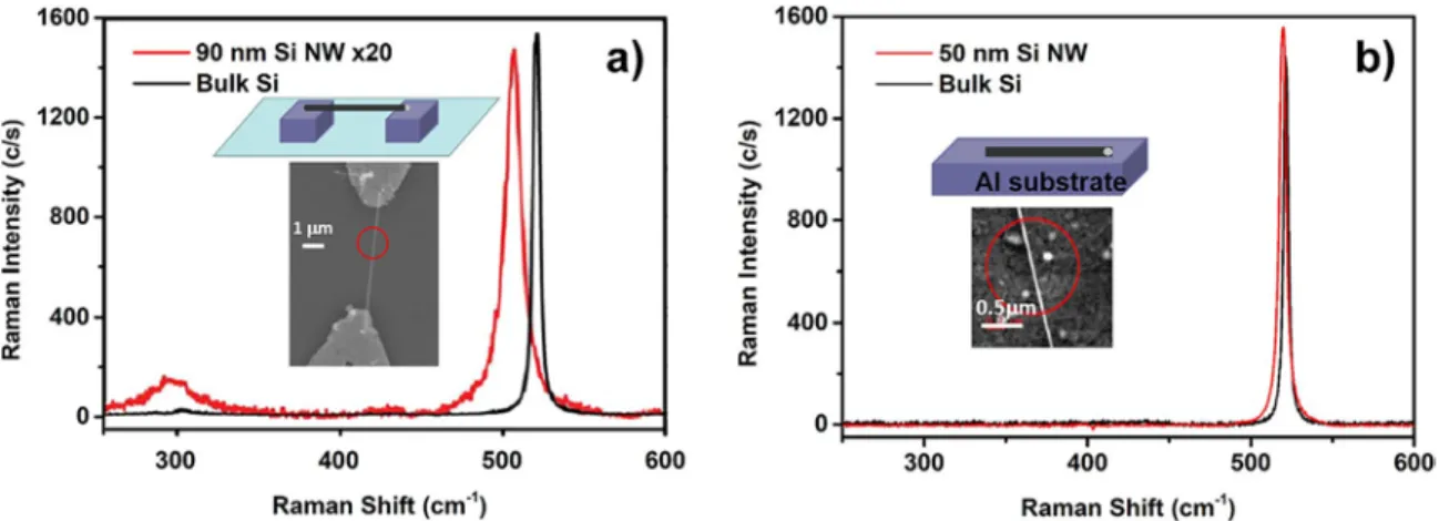
The Raman spectrum of a Si NW compared to the Raman signal arising from bulk Si obtained under the same experimental conditions is shown in Figure 1. Figure 1a compares the spectrum of the free standing NW with respect to that of bulk Si. The typical Raman signature of Si at high temperature is observed in the free standing NW, with a clear downshift with respect to the 300 K Si Raman frequency. In Figure 1b the spectrum of the NW deposited on an Al substrate and that of bulk Si are shown, all of them obtained under the same
Figure 1. a) Raman spectra of a free standing Si NW and a bare Si bulk substrate, (b) Raman spectra of a Si NW deposited on a metallic substrate and a
ffi
�
excitation conditions. Interestingly, the two Raman signals are roughly equivalent in this case, in spite of a scattering volume ratio of near 100 times between bulk and NW when excited with a focused laser beam with a diameter of 1 μm. Therefore, taking into account the corresponding scattering volumes it is possible to estimate an enhancement in the Raman intensity per unit volume of roughly a factor 100 in the NW with respect to the bulk material. This resonance behavior allows achieving exhaustive Raman studies using individual semiconductor NWs. Note that the Al substrate enhances the Raman signal of the NW with respect to the Raman signal of the free standing NW, and effectively dissipates the heat generated by the laser beam absorption.
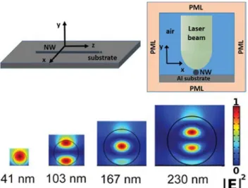
Modeling the EM interaction between the laser beam and the NWs is the complement to the micro-Raman experiments. This model is solved by FEMs using COMSOL Multiphysics. The Maxwell equations are solved for the NW and its surrounding space when excited by a focused laser beam in similar conditions to the micro-Raman experiments.[16,20] The system formed by the air/NW/substrate was limited by cartesian perfectly matched layers (PMLs), which absorb the outgoing radiation eliminating secondary reflections, Figure 2. The complex refractive indexes used in the calculations were taken from Sopra database.[21] Details of the calculation procedure are in refs. [16] and [20].
The solution of the model provides the EM field intensity, |E|2,
distribution inside the NW. Since The Raman signal is directly proportional to the field intensity |E|2, it is possible to analyze the Raman signal arising from the NW in terms of |E|2 to compare it to the experimental values. In the case of homogeneous NWs this can be achieved by using a two dimensional (2D) model because of the axial symmetry, which allows to calculate the distribution of the electric field inside the NW as a function of the NW diameter, as we show in Figure 2.
Figure 2. Scheme of the 2D modeling of the system NW/Substrate/laser
beam, the PLMS are perfect matching layers (upper panel). Calculated electromagnetic field intensity distribution inside Si NWs of different diameters deposited on an Al substrate. The simulation is done for a Gaussian laser beam with wavelength of 532 nm. The black circles represent the perimeter of the NWs with different diameters (lower panel).
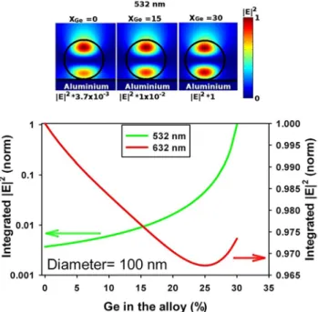
The electric field distribution exhibits different patterns depending on the NW diameter. For diameters around 40 nm a nearly radial symmetry distribution is observed; for increasing diameters the electric field presents a lobular distribution with two or more lobes depending on the NW diameter. If one integrates the electric field to the full NW section one observes diameter resonances of |E|2, which depend on the laser wavelength and the composition of the NW. The role of the NW composition is shown in Figures 3 and 4, where the electric field was calculated for different SiGe NW compositions. The field distribution is similar for all of them, but the integrated intensity decreases with the Ge content for 532 nm light excitation, while it presents the opposite behavior for excitation with 632 nm. This holds for a NW diameter of 50 nm, Figure 3. For different diameters the results change, for example, for a diameter of 100 nm the opposite behavior happens, as shown in Figure 4.
In certain SiGe NWs the Raman spectrum reveals the existence of inhomogeneous composition inside the NW, with pure Ge regions in the NWs as shown in Figure 5, where one can appreciate the Raman peak of pure Ge (300 cm-1), together with the SiGe related bands . It should be noted that in SiGe it is frequently observed the segregation of Ge because of the Si oxidation creating a germanium rich layer.[21,22] What is
interesting here is that the Raman band associated with pure Ge ( 300 cm-1) modifies its intensity depending on the transversal position of the laser beam with respect to the NW axis. To analyze this behavior we modeled the NW as a core-shell structure with a thin shell of segregated pure Ge. The |E|2
Figure 3. Calculated electromagnetic field intensity distribution inside an
�
Figure 4. Calculated electromagnetic field intensity distribution inside a
SiGe NW (100 nm diameter) as a function of the Ge content (%) for an excitation wavelength of 532 nm (upper panel). Integrated intensity versus Ge content for 532 and 632 nm excitations (lower panel).
distribution inside the NW ( 85 nm diameter) is not homoge- neous; in particular, it looks like two spatially opposed lobes strongly localized near the NW outer shell. This region in which |E|2 is strongly localized will contribute the most to the Raman signal, being possible to explain the anomalous Raman spectrum by the presence of a Ge rich outer shell, which the contribution to the Raman signal is overrepresented because of the |E|2 distribution. In Figure 5 we also show the results of the simulated laser cross walk experiment. This simulation shows that the localized |E|2 distribution lobes rotate when the laser beam position across the NW changes, therefore, the Raman signal arises from different zones of the NW outer shell depending on the transverse laser position with respect to the NW axis, Figure 5. Therefore, the variation of the Ge related Raman band intensity with respect to the position of the laser beam across the NW suggests that the Ge rich outer shell is non- homogeneous. The rotation of the localized |E|2 lobes and the
non uniformity of the Ge-rich layer can explain why the Raman spectra of the NW can be different for the three transverse positions of the laser beam represented in Figure 5, even when a similar volume of the NW is being probed for the three laser beam positions (Supporting Information). The inhomogeneous Ge rich outer shell can be due to the oxidation of the NW,[22,23] but also to parasitic nucleation of Ge. The transmission electron microscopy (TEM) image and transverse electron dispersive X-Ray spectroscopy (EDX) scan of an SiGe NW are shown in Figure 6, showing the existence of a non uniform Ge rich outer shell.
The presence of the axial heterojunction breaks the longitudinal symmetry of the NW. Therefore, a 3D model must be applied, instead of the 2D model used for NWs
Figure 5. a) AFM image of a SiGe NW (85 nm diameter). The three circles
correspond to the transversal positions of the laser beam. b) Raman spectra for the three positions of the laser beam, and field intensity distribution calculated for each of the three configurations, showing the rotation of the field pattern with the position of the laser beam with respect to the NW axis.
without axial discontinuities, either homogeneous NWs or core/shell heterostructured NWs.[16,20] The 3D model accounts for the presence of the axial HJ; and also takes account of the finite length of the NW. The modeled system consists of an axially heterostructured NW deposited on a metallic (Al) substrate, surrounded by air and illuminated by the 532 nm laser line focused on the NW by the microscope objective, in a similar configuration as the one used in the Raman experiments (Figure 7).
Figure 6. TEM image of a NW showing Ge rich clusters in the NW periphery
� Figure 7. 3D model used for solving the interaction between the laser
beam and the heterostructured NW.
The axial heterojunction in SiGe/Si NWs is not abrupt. The transition between the two NW segments is not sharp, but it appears as a region with graded composition in between those of the two segments.[14,15] Usually, it is assumed to have a thickness of the order of the NW diameter; although, it is more appropriate to say that the HJ width is a fraction of the NW diameter; which depends on the growth conditions.[24] Therefore, when the laser beam impacts on the HJ is probing the Si segment, the SiGe segment, and the HJ itself. These three regions of different composition shall contribute to the Raman spectrum. The Raman spectra of the heterostructured NWs are recorded along the NW axis in steps of 100 nm. The spectra recorded on the homogeneous Si and SiGe segments show the typical Lorentzian peaks, with the spectral parameters characteristic of Si and SiGe pure NWs,
respectively. Meanwhile, the spectra obtained when the laser beam shares the HJ and the neighboring NW segments appear broadened and asymmetric, Figure 8. Furthermore, the overall Raman intensity is enhanced with respect to the
Figure 8. Raman spectrum obtained when the laser beam shares the two
NW segments and the HJ. The three peaks obtained by deconvolution of the spectrum correspond to the SiGe segment, the HJ itself and the Si segment. (λexc ¼ 532 nm).
homogeneous segments. This is the consequence of the overlapping between the Raman contributions arising from the different regions of the NW probed by the laser beam. The spectral deconvolution reveals the contribution to the experimental Raman band of the two NW segments, Si and SiGe, and an additional Raman peak arising from the HJ itself. When this deconvolution is done with only two Raman peaks, those corresponding to the two homogenous segments, one cannot achieve a satisfactory fitting of the Raman spectrum. It is necessary to add a third peak to achieve the fitting of the Raman spectrum of the region including the HJ. This third peak has spectral characteristics in between those of the Si and SiGe segments of the NW. It arises from the HJ itself, which is a compositionally graded NW rod. It is important to recall that the HJ width is close or below to the NW diameter ( 50 nm in this case),[14,15,24] while the excited length of the two homogeneous segments of the NW lies around 500 nm
Figure 9. a) Experimental Raman profiles along a heterostructured Si/ SiGe
(approximately half of the laser spot diameter) for a laser beam centered on the HJ. As a result, the probed volume of each of the homogeneous segments is at least 10 times larger than that of the HJ; however, the intensity of the Raman signal associated with the HJ is of the same order of magnitude, or even higher, as the signals arising from the homogeneous segments, see Figure 8. Translating this result into Raman intensity per unit of scattering volume, it results in an enhancement of 10–20 times in the HJ region with respect to the homogeneous segments, depending on the studied NW. In ref. [16] one can see the spectrum at the HJ of a SiGe/Si axially heterostructured NW with higher concentration of Ge (60%), where one can clearly appreciate the HJ contribution. The calculated results obtained from the solution of the EM model were contrasted to the experimental results. The Raman intensity profiles along the NW axis are plotted in Figure 9, where one establish the comparison between the experimental Raman profile, Figure 9a, showing the Raman intensity of the Si segment, the SiGe segment, and the HJ, as a function of the laser beam position; andthe calculated Raman profile. The Raman intensity is proportional to |E|2, which is obtained from the distribution of the electric field along the NW by integrating over the volume of the NWprobedby thelaserbeamateachbeamposition, Figure 9b. The Raman profiles evidence the signal enhancement that takes place at the HJ. We can see that the signal of the HJ region is comparable to that of the homogeneous segments, despite the difference of a factor 10 in probed volume, as it was aforementioned. The simulations are in good agreement with the experimental measurements, reproducing the Raman experiments and the EM enhancement effect. Note that the spread out of the Raman signal around the HJ is due to the size of the laser beam. The decrease of the Raman intensity of the Si and SiGe segments toward the ends is due to the fact that the laser beam is partially out of the NW. The NW studied in Figure 9 was longer on the Si side than in the SiGe side. One observes the decrease of the Raman intensity fromthe SiGe segmentwhenlaser beamstartsto overrun the NW end.
4. Conclusions
We have described the main effects resulting from the interaction between group IV semiconductor NWs and a focused laser beam. The influence of the NW diameter, NW composition, NW structure, in particular axially heterostruc- tured SiGe/Si NWs, on the optical response of the NWs has been studied by both experimental micro-Raman spectros- copy, and the FEM solution of the Maxwell equations. Both experimental and modeling results are in good agreement, and permit to account for the very interesting optical properties of the NWs. The sensitivity of the optical properties of the NWs to those geometric, compositional, and structural factors suggests a great potential of the NW for photon handling.
Supporting Information
Supporting Information is available from the Wiley Online Library or from the author.
Acknowledgments
This work was funded by Junta de Castilla y Leo'n (Project VA293U13), J. L
Pura was granted by Spanish Government, FPU program (FPU14/00916).
Conflict of Interest
The authors declare no conflict of interest.
Keywords
axially heterostructured nanowires, group IV semiconductor nanowires, light/ nanowire interaction, optical resonances, Raman spectroscopy
Received: April 27, 2018 Revised: July 13, 2018 Published online:
[1] G Bronstrup, N. Jahr, C. Leiterer, A. Csaki, W. Fritzsche,
S. Christiansen, ACS Nano 2010, 4, 7113.
[2] M. Law, D. J. Sirbuly, J. C. Johnson, J. Goldberger, R. J. Saykally, P. Yang, Science 2004, 305, 1269.
[3] H. Kallel, A. Arbouet, G. Bensssayag, A. Chehaidar, A. Poti'e,
B. Salem, T. Baron, V. Paillard, Phys. Rev. B 2012, 86, 085318.
[4] L. Cao, P. Fan, A. P. Vasudev, J. S. White, Z. Yu, W. Cai, J. A. Schuller,
S. Fan, M. L. Brongersma, Nano Lett. 2010, 10, 439.
[5] L. Cao, J. S. White, J. S. Park, J. A. Schuller, B. M. Clemens,
M. L. Brongersma, Nature Mater. 2009, 8, 643.
[6] R. Ruppin, J. Opt. Soc. Am 1998, 15, 1891.
[7] L. Cao, B. Nabet, J. E. Spanier, Phys. Rev. Lett. 2006, 96, 57402.
[8] G. S. Doerk, C. Carraro, R Maboudian, ACS Nano 2010, 4, 4908.
[9] F. J. Lopez, J. K. Hyun, U. Givan, I. S. Kim, A. L. Holsteen, L. J. Lauhon, Nano Lett. 2012, 12, 2266.
[10] Z. Zhang, D. C. Dillen, E. Tutuc, E. T. Yu, Nano Lett. 2015, 15, 4303.
[11] D. C. Dillen, K. M. Varahmyan, C. M. Corbet, E. Tutuc, Phys. Rev. B
2012, 86, 045311.
[12] J. Anaya, A. Torres, A. C. Prieto, V. Hortelano, J. Jim'enez,
A.Rodríguez, T. Rodríguez, Appl. Phys. A 2014, 114, 1321.
[13] M. Kerker, The Scattering of Light and Other Radiations. Academic
Press, New York 1969.
[14] T. E. Clark, P. Nimmatoori, K. K. Lew, L. Pan, J. M. Redwing,
E. C. Dickey, Nano Lett. 2008, 8, 1246.
[15] P. Periwal, N. V. Sibirev, G. Patriarche, B. Salem, F. Bassani,
V. G. Dubrovskii, T. Baron, Nano Lett. 2014, 14, 5140.
[16] J. L. Pura, J. Anaya, J. Souto, A. C. Prieto, A. Rodríguez, T. Rodríguez,
P. Periwal, T. Baron, J. Jim'enez, J. Appl. Phys 2018, 123, 114302.
[17] D Li, Y Wu, P Kim, L Shi, P. Yang, A. Majumdar, Appl. Phys. Lett. 2003,
83, 2934.
[18] J. Anaya, T. Rodríguez, J. Jim'enez, Sci. Adv. Mater. 2015, 7, 1097.
[19] A. Torres, A. Martín-Martín, O. Martínez, A. C. Prieto, V. Hortelano,
J. Jim'enez, A. Rodríguez, J. Sangrador, T. Rodríguez, Appl. Phys. Lett
2010, 96, 011904.
[20] J. L. Pura, J. Anaya, J. Souto, C. Prieto, A. Rodríguez, T. Rodríguez,
J. Jim'enez, Nanotechnol. 2016, 27, 455709.
[21] Sopra database S A, France. www.sspectra.com/sopra
[22] F. K. Le Goues, R. Rosenberg, T. Nguyen, F. Himpsel, B. S. Meyerson,
J. Appl. Phys. 1989, 65, 1724.
[23] N. Sugiyama, T. Tezuka, T. Mizuno, M. Suzuki, Y. Ishikawa,
N. Shibata, S. Takagi, J. Appl. Phys. 2004, 95, 4007.
[24] J. L. Pura;, P. Periwal, T. Baron, J. Jiménez, Nanotechnol. 2018, 29,