MINIMUM AREA, LOW COST FPGA IMPLEMENTATION OF AES
Liberatori, Mónica. Bonadero, Juan Carlos.
Facultad de Ingeniería. Universidad Nacional de Mar del Plata Laboratorio de Alta Frecuencia
Juan B. Justo 4302. Mar del Plata (7600). Bs. As. Argentina.
ABSTRACT
The Rijndael cipher, designed by Joan Daemen and Vincent Rijmen and recently selected as the official Advanced Encryption Standard (AES) is well suited for hardware use. This implementation can be carried out through several trade-offs between area and speed.
This paper presents an 8-bit FPGA implementation of the 128-bit block and 128 bit-key AES cipher. Selected FPGA Family is Altera Flex 10K. The cipher operates at 25 MHz and consumes 470 clock cycles for algorithm encryption, resulting in a throughput of 6.8 Mbps. The design target was optimisation of area and cost.
Keywords: AES, cipher, cryptography, FPGA,
VHDL.
1. INTRODUCTION
The Rijndael Algorithm, developed by Joan Daemen and Vincent Rijmen [1], has been approved by the U. S. National Institute of Standards and Technology (NIST) as the was the new Advanced Encryption Standard (AES). It became official in October 2000, replacing DES [2]. As this block cipher is expected to be widely used in an extensive variety of products, its efficient implementation becomes a significant priority. It is a private-key symmetric block cipher, [16], [17], operating on a block size of 128 bits. It comprises 10, 12 or 14 rounds when the key size is 128, 192 or 256 bits respectively. The intermediate cipher result is called the state [1].
Figure 1 – Input to, and output from, the cipher state
array.
It is an array of 4 rows and Nc columns, where Ncis
the input sequence length divided by 32. In this state
array, denoted by the symbol s, each individual byte
has two indexes: its row number r, in the range 0 ≤ r
< 4, and its column number c, in the range 0 ≤ c < Nc, hence allowing it to be referred as s[r, c]. For
AES the range for c is 0 ≤ c < 4, since Nc has a fixed
value of 4. At the start (end) of an encryption or decryption operation the bytes of the cipher input (output) are copied to (from) this state array in the
order shown in Fig. 1. The four bytes in each column of the state can be thought of as an array of
four bytes indexed by the row number r or as a
single 32-bit word (bytes within all 32-bit words will
always be enumerated using the index r). The state
can hence be considered as a one-dimensional array
of words where the column number c provides the
array index.
The round function is parameterised using a Round
Key that consists of a Nc word sub-array from the
key schedule. In general the length of the cipher
input, the cipher output and the cipher state, Nc,
measured in multiples of 32 bits, is 4, 6 or 8 but the AES standard only allows a length of 4. The length of the cipher key, Nk, again measured in multiples of
32 bits, is also 4, 6 or 8, all of which are allowed by both Rijndael and the AES standard.
Each encryption round is composed of four operations: SubBytes, ShiftRows, MixColumns and KeyExor. The last round is slightly different because MixColumns is not present.
[image:1.595.72.289.554.670.2]SuBytes transformation is a non-linear byte substitution where each byte of the state is inverted over GF(28) followed by an affine transformation. The overall operation is known as the S-Box and can be performed through a look up table as depicted by Fig. 2 [12], [13].
Figure 2 – SubBytes Transformation
ShiftRows transformation operates on a whole state
(128 bits). Rows of the state are cyclically shifted to
the left as shown in Fig. 3.
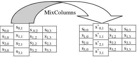
MixColumn transformation acts independently on
every column of the state and treats each column as
in0 in4 in8 in12
in1 in5 in9 in13
in2 in6 in10 in14
in3 in7 in11 in15
s0,0 s0,1 s0,2 s0,3
s1,0 s1,1 s1,2 s1,3
s2,0 s2,1 s2,2 s2,3
s3,0 s3,1 s3,2 s3,3
out0 out4 out8 out12
out1 out5 out9 out13
out2 out6 out10 out14
out3 out7 out11 out15
s0,0 s0,1 s,0,2 s0,3
s1,0 s1,1 s1,2 s1,3
s2,0 s2,1 s2,2 s2,3
s3,0 s3,1 s3,2 s3,3
s0,0 s0,1 s0,2 s0,3
s1,0 s1,1 s1,2 s1,3
s2,0 s2,1 s2,2 s2,3
s3,0 s3,1 s3,2 s3,3 s’1,1
s1,1
[image:1.595.310.538.585.663.2]a four-term polynomial. The columns of the state are
considered as polynomials over GF(28) and
multiplied modulo (x4+ 1) with a fixed polynomial
c(x), coprime to x4+ 1 and therefore invertible [14].
[image:2.595.63.292.256.351.2]This operation can be written as a matrix multiplication and is represented in Fig. 4.
Figure 3 – ShiftRows Transformation
Figure 4 – MixColumns Transformation
2. GENERAL ASPECTS
As is the case with software, hardware implementations can be optimized in speed and size. However, size usually translates much more directly into cost in hardware when compared to software. Doubling the size of an encryption program may make little difference on a general-purpose computer with a large memory, but doubling the area used in a hardware device will likely more than double the cost of the device.
A promising alternative for implementation consists of reconfigurable hardware devices such as Field Programmable Gate Arrays (FPGAs) [4], [5], [8]. FPGAs comprise an array of uncommitted circuit elements, called logic blocks, and interconnected resources. FPGAs configuration is performed by the end user, facilitating design changes. This new technology offers many advantages for designers of cryptographic equipment due to its high flexibility, low development costs and physical security.
The FPGA family selected For the present implementation is Altera Flex 10K, in particular EPF10K20. It is well suited for memory functions and complex logic functions such as digital signal processing and data transformation. The EPF10K20 device contains an embedded array to implement memory functions and a logic array to implement general logic functions. The device has 1152 logic elements (LEs) and 6 embedded array blocks (EABs). Each LE consists of a 4-input look up table (LUT), a programmable flip-flop, and dedicated signal paths for carry and cascade functions. LEs are
grouped into 144 LABs. These LABs are arranged into 6 rows and 24 columns. The embedded array consists of a series of EABs, each of which provides 2048 bits of memory, and can be used to create RAM or ROM or to contribute 100 to 300 gates toward combinatorial logic functions. Each I/O cell contains a bi-directional I/O buffer and a flip-flop that can be used as either an input or output register. In this case, the device is part of the UP1 Educational Board of the University Program Design Laboratory Package from Altera. MAX+PLUS II Version 7.21 Student Edition is the software used to synthesise a VHDL implementation of the AES algorithm. This tool is also used to perform behavioural and timing simulations.
3. ARCHITECTURE OPTIONS
Rijndael is a block cipher with a basic looping architecture whereby data is iteratively passed through a round function. There are several architectural options to yield optimised implementations [3].
When examining AES principal aspects, it is obvious that an implementation of the fully 128 data path stream could encrypt 128 bits per cycle. Assuming a 25 MHz clock, this translates into a throughput of 3.2Gps. Such an implementation will also consume too many resources in terms of area. It will require a large amount of I/O pins and will not fit on low target FPGA. Since the EPF10k20 is available in 240-pin RQFP package, it is not suitable for this type of architecture.
On the other hand, in a minimum configuration, the cipher should use as few memory blocks as possible and a basic interface with a host system as to allow its adaptation to a wide range of proposals. Since one byte is the basic data unit for the Rijndael operations, the architecture selected to implement the cipher is an 8 bit basic one.
After defining the bit-width of the architecture, the next problem is determining a set of operation types that will define the functional units. A first analysis of the algorithm identifies primary operations, which leads to the development of the functional units needed. This design strategy is a hierarchical one, where the basic blocks are implemented and then composed to obtain the cipher.
In the encryption core, only one round is implemented and the cipher must iterate ten rounds to perform an encryption. Iterative looping (LU-1) is a subset of loop unrolling (LU-i) where only one round is unrolled. This approach usually minimizes the hardware required for the implementation and an effort is made to maximize the speed.
Thus, one round is implemented with combinatorial logic supplemented with registers, memories and multiplexers. First, input block of data is fed to the circuit via the 8-bit input interface and the initial
round is executed. In this round the input data is
s0,0 s0,1 s,0,2 s0,3
s1,0 s1,1 s1,2 s1,3
s2,0 s2,1 s2,2 s2,3
s3,0 s3,1 s3,2 s3,3
s0,0 s0,1 s0,2 s0,3
s1,1 s1,2 s1,3 s1,0
s2,2 s2,3 s2,0 s2,1
s3,3 s3,0 s3,1 s3,2
s0,0 s0,1 s,0,2 s0,3
s1,0 s1,1 s1,2 s1,3
s2,0 s2,1 s2,2 s2,3
s3,0 s3,1 s3,2 s3,3
s0,0 s0,1 s0,2 s0,3
s1,0 s1,1 s1,2 s1,3
s2,0 s2,1 s2,2 s2,3
s3,0 s3,1 s3,2 s3,3 MixColumns
s0,1
s1,1
s2,1
s3,1
s’0,1
s’1,1
s’2,1
XORed with the Cipher Key and the result stored in
a RAM memory. Then the encryption unit evaluates
ten rounds of the algorithm and the result is
temporarily stored in the RAM. A control unit
generates control signals for the other units, answering the question of the separation between control and data path logic.
The provided embedded RAM is used to replace the round key and S-Box hardware. As a result, there is no key scheduling unit; instead a memory for storing
the internal keys and the circuitry necessary to distribute these keys is included in the encryption unit.
The mode of operation is very simple: electronic codebook (ECB). The basic architecture in conjunction with the non-feedback mode of operation is easy to implement and will likely result in smaller circuit area.
The cipher was designed keeping in mind the amount of resources shared between encryption and decryption, so that a modified version will support both types of operation [10].
The simulations verify the ability to operate at the 25 MHz system clock frequency of the UP1 Educational Board. The design choice is a compact one, optimized for area and cost.
4. FPGA IMPLEMENTATION
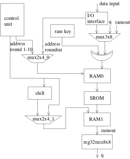
[image:3.595.312.519.411.555.2]The round transformation data path is shown in Fig.5.
reg32mix8x8 RAM1 mux2x4_1
SROM shift
RAM0 data input
I/O interface
mux3x8 q ramout
mux2x4_0
ram key
ramout
q address
round 1-10 address roundini control
unit
Figure 5 – The 8-bit round transformation data path.
It consists of two 16x8 RAMs (RAM0 and RAM1),
one 256x8 ROM (SROM), one block to perform
MixColumns operation with interfaces for the 8 bit
bus (reg32mix8x8), another component to perform
the shift operation (shift), one 8-bit exor and three
multiplexers (mux2x4_0, mux2x4_1 and mux3x8).
Round Keys for encryption are loaded via the input
interface and are stored in the 256x8 RAM
(ramkey). All keys are loaded before encryption
begins. The control unit is a finite state machine. It
provides multiplexer select signals and generates control signals for the previously mentioned round components.
RAM0 receives the 128 bit input data from initial
round. It also stores the results of intermediate rounds and the 128 bits final encrypted block. It is accessible via an 8-bit data bus in a sequential manner, acting like a 128-bit register. The encryption process starts after reception of the forth 128 data bits.
SROM performs byte substitution and acts as one
S-Box, storing the overall transformation needed in 8 x 256 bits. It is implemented using one EAB block. An 8-bit address is the data input and an 8-bit data value is the output.
The results from the SubBytes operation are temporarily stored in RAM1. This memory is written so that SubBytes and ShiftRows operations
are combined. The component mux2x4_1 presents
the appropriate address bus to the RAM1 memory. The execution of these transformations modifies the
address coming from the control unit via the shift
component as it is depicted in Fig. 6.
out1 out2
out3out4 shift
in1 in2 in3 in4
Figure 6 – Shift Component.
Reading from SROM
Writing
RAM1 Reading from
SROM
Writing RAM1
Byte 0 Address 0 Byte 8 Address 8
Byte 1 Address D Byte 9 Address 5
Byte 2 Address A Byte 10 Address 2
Byte 3 Address 7 Byte 11 Address F
Byte 4 Address 4 Byte 12 Address C
Byte 5 Address 1 Byte 13 Address 9
Byte 6 Address E Byte 14 Address 6
Byte 7 Address B Byte 15 Address 3
Table 1. ShiftRows Transformation.
[image:3.595.70.283.426.686.2]The shift component generates the addresses in
RAM1 to be written to. Table 1 presents the order in which the successive bytes from the SubBytes
operation are written to RAM1 [9]. The control unit
generates the addresses in RAM1 to be read from. The reading process is a direct one.
The MixColumn transformation previously described can be written as a matrix multiplication, where the matrix is a circular one:
=
c 3, c 2, c 1, c 0, c 3, c 2, c 1, c 0,s
s
s
s
02
01
01
03
03
02
01
01
01
03
02
01
01
01
03
02
s'
s'
s'
s'
Eq.(1)As a result, the four bytes in the column can be replaced by the following expressions:
c 3, c 2, c 1, c o, c
o,
({02}.s
)
({03}.s
)
s
s
s'
=
⊕
⊕
⊕
c c c
c
c
s
s
s
s
s
'
1,=
0,⊕
({
02
}.
1,)
⊕
({
03
}.
2,)
⊕
3,)
}.
03
({
)
}.
02
({
'
2,cs
0,cs
1,cs
2,cs
3,cs
=
⊕
⊕
⊕
)
}.
02
({
)
}.
03
({
'
3,cs
0,cs
1,cs
2,cs
3,cs
=
⊕
⊕
⊕
Four inputs
s
0,c,s
1,c,s
2,c,s
3,c, are multipliedwith fixed constants. Multiplication by a constant in
GF(28) will result in XOR the bits of the input byte
in a particular way [6], [7].
Multiplication by x (i.e. 00000010 or {02}) can be
implemented at the byte level as a left shift and a subsequent conditional XOR with {1B}. This
operation on bytes is denoted by xtime() and it can
[image:4.595.311.524.105.226.2]be easily implemented in FPGA as it is depicted in Fig. 7. 1B b7 b6..b0 8 8 7
inxtime s outxtime
xtime
Figure 7 – Xtime Operation
Multiplication by higher powers of x can be
implemented by repeated application of xtime().
Multiplication by (1+x) (i.e. 00000011 or {03}) can
be thought as multiplication by ({01}
⊕
{02}). Fig.8 presents a circuit that implements this operation.
1B b7 b6..b0 8 8 7 xtime outx3 inx3 8 8
[image:4.595.74.255.188.259.2]Figure 8 – X3 Operation
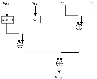
Fig. 9 shows the basic block to perform
MixColumns operation, multcolumn. Four
components like those shown in Fig. 9, each with its entries consistent with Eq (1) or its equivalent expressions, are needed to process 32-bit data simultaneously. As it can be seen from this figure, the critical path through this transformation includes four XORs and one multiplexer. To generate four
bytes in one operation, reg32mix8x8 accepts four
bytes from input via a serial to parallel converter register. The result, one column of the state generated from each input column, must be converted to the serial form to fit in the original 8-bit data path.
Figure 9 – MixColumn basic block: multcolumn.
Each 8-bit word from the input is processed as follows. The initial round performs the XOR operation between the 128-bit data and the original 128-bit key. The result is stored in RAM0.
Every round starts by reading this memory and presenting every byte out to the address input of the SROM. One cycle later the result of the SubBytes transformation for every byte of the State is presented at the output of the SROM. These 16 bytes are written in RAM1 as shown in Table 1. Another 16 cycles are taken to read the result of the
s0,c s1,c s2,c s3,c
xtime x3
[image:4.595.313.513.441.604.2] [image:4.595.70.269.575.690.2]ShiftRows operation. At the same time the MixColumns operation is performed on every 4-bytes word of this stream. This transformation results in a latency of 10 cycles because of the initial serial to parallel and final parallel to serial conversions needed to preserve the 8-bit data path. The stream of bytes resultant from this last operation is XOR with the appropriate bytes of the round key. The result is stored in the RAM0, ready to initiate another round of the cipher.
5. RESULTS FOR THE ALTERA 10K FAMILY
The parameters used for evaluating the quality of the implementation are: number of logic cells (LCs), number of bits of embedded memory, latency, clock frequency and throughput.
The process previously explained involves 48 clock cycles to complete one round of encryption, except for the last one that consumes 38 cycles because it does not include the MixColumn operation. These numbers translate into 470 total cycles, resulting in a throughput of 6.8 Mbps.
The results of the implementation in terms of area are summarized in Table 2. All the results come from simulations and reports generated by Altera tools.
Component Memo Bits
Memo Used
%
LCs LCs Used%
I/O interface --- --- 62 10
ROM 256x8 2048 33 --- ---
RAM 16x8 128 2 --- ---
Mux 3x8 --- --- 24 4
Mux 2x4 --- --- 4 0
Mux 2x8 --- --- 8 1
Control Unit --- --- 305 52
Shift --- --- 4 0
Reg32mix8x8 --- --- 160 27
AES cipher 4480 36 581 50
In terms of complexity, the operation that requires more hardware resources as well as computation time is the MixColumns multiplication. Fast operations such as bit-wise XOR and ShiftRows are constructed from simple hardware elements. The S-Box is implemented by 256x8 ROM. Round Keys are stored in 256x8 RAM. Additional memory is used to store partial results of intermediate operations. 36% of memory blocks are used to cover the whole 128-bit data processing,.
6. CONCLUSIONS
When implementing block ciphers, the designer must choose between several strategies. He or she has to decide whether to optimize for area, throughput or latency. Each design choice imposes different restrictions on the final implementation. This paper presents a low area, cost-effective Rijndael cipher for encryption using a basic 8-bit
iterative architecture, targeted towards the Altera Flex 10 K family of FPGAs.
The cipher has been synthesised using Altera. MAX+PLUS II Version 7.21 Student Edition [19], [20]. The algorithm is implemented in VHDL, which led to the use of bottom-up design and test methodology [15], [18]. This choice also insures portability of the code to the devices of other vendors.
The VHDL code was simulated using the test vectors provided in the AES submission package. The results are functionally correct.
The architecture needs fewer logic cells than other ciphers and uses as few memory blocks as possible [11]. It has 6.8 Mbps throughput. The critical path includes the components previously mentioned. The minimum clock period depends on the access time to memories used and the frequency of the external clock.
Future work should concentrate on speed performance and the introduction of pipelines in the architecture.
7. REFERENCES
[1]J. DAEMEN, V. RIJMEN, AES Proposal:
Rijndael. Document version 2. Date: 03/09/99. NIST´s AES home page, http://www.nist.gov/aes.
[2]FEDERAL INFORMATION PROCESSING
STANDARDS PUBLICATION (FIPS) 197. Specification for the Advanced Encryption Standard (AES). November 26, 2001. NIST´s AES home page, http://www.nist.gov/aes.
[3]E. BIHAM, A note on Comparing the AES
Candidates. Second AES conference, 1999.
[4]K. GAJ, P.CHODOWIEC, Comparison of the
hardware performance of the AES candidates using reconfigurable hardware. Proceedings of RSA Security Conference - Cryptographer's Track, San Francisco, CA, 2001 April 8-12, pp. 84-99.
[5]A. ELBIRT, W. YIP, B. CHETWYND, C.
PAAR, An FPGA Implementation and Performance Evaluation of the AES block cipher candidates algorithm finalists. IEEE Transactions on Very Large Scale Integration (VLSI) Systems, August 2001, pp. 545-557.
[6]T. KERINS, A. PPOPOVICI, A. DALY, W.
MARNANE, Hardware encryption engines for e-commerce. Proceedings of Irish Signals and Systems Conference, 2002, pp 89-94.
[7]J. SHIM, D. KIM, Y. KANG, T. KWON, J.
CHOI, Inner-pipelining Rijndael cryptoprocessor with on-the-fly key scheduler. http://www.ap-sic.org/2002/proceedings/2B/2B-3.PDF.
[8]V. FISCHER, Realization of the round 2 AES
http://csrc.nist.gov/encryption/aes/round2/conf3 /aes3papers.html. March 2000.
[9]R. KARRI, Y. KIM, Field Programmable Gate
Array implementation of Advanced Encryption Standard. http://www.eeweb.poly.edu/dream-it/publications/Rijndael.pdf
[10]R. ASHRUF, G. GAYDADJIEV, S.
VASSILIADIS, Reconfigurable implementation for the AES algorithm. Computer Engineering Laboratory, Electrical Engineering Department, Delft University of Technology, http://ce-serv.et.tudelft.nl/~molen/publications/2002/ash/ ash_prorisc2002.pdf.
[11]P. MROCZKOWSKI, Implementation of the
block cipher Rijndael using Altera FPGA. http://csrc.nist.gov/encryption/aes/round2/comm ents/200 00510-pmroczkowski.pdf (Aug. 2001).
[12]A. RUDRA, K. DUBEY, C. JUTLA, Efficient
implementation of Rijndael encryption with composite field arithmetic. Workshop on Cryptographic Hardware and Embedded Systems, CHES 2001, May 13-16, Paris, France.
[13]V. RIJMEN, Efficient Implementation of the
Rijndael S-Box. CHES 2003, LNCS 2779, pp 334-350.
[14]S. MURPHY, M. ROBSHAW, Essential
Algebraic Structure within AES. Second NESSIE. New European Schemes for Signature, Integrity and Encryption Workshop. September 2001.
[15]An Introductory VHDL Tutorial.
http://www.gmvhdl.com/VHDL.html.
[16]STALLINGS W., Cryptography and Network
Security, 2nd Edition, 1999. Prentice Hall.
[17]SCHNEIER B., Applied Cryptography, John
Wiley & Sons, Inc., second edition, 1996.
[18]F. PARDO, J. BOLUDA, VHDL. Lenguaje
para síntesis y modelado de circuitos. Editorial Ra-Ma. Edición 1999.
[19]L. TERÉS, Y. TORROJA, S. OLCOZ, E.
VILLAR. VHDL. Lenguaje Estándar de Diseño Electrónico. Editorial Mc Graw Hill/Interamericana de España, S.A.U. 1997.
[20]MAX+PLUS II. Programmable Logic
![Fig. 2 [12], [13].](https://thumb-us.123doks.com/thumbv2/123dok_es/4592697.43166/1.595.72.289.554.670/fig.webp)