Energy processing by means of power gyrators
150
0
0
Texto completo
(2)
(3) Als meus pares, Angel i Pilar. A la meua companya Laura. i.
(4) ACKNOWLEDGEMENT (In Catalan) En primer lloc, vull expressar la meua gratitud a Luis Martinez Salamero, director d’aquesta tesi, pels seus consells, orientació, per tot el que he après treballant al seu costat i per la seua generositat. Gràcies també a Francesc Guinjoan Gispert membre del Department d’Enginyeria Electrònica de la Universitat Politècnica de Catalunya per la tutoria d’aquesta tesi. Igualment, gràcies a Corinne Alonso del Laboratoire d’Analyse et d’Architecture des Systèmes de Toulouse i a Jean Alzieu i Guy Schweitz d’Electricité de France R&D per permetre’m realitzar aquest treball de recerca en les millors condicions. Destacaré aquí la professionalitat de tots els professors del Departament d’Enginyeria Electrònica Elèctrica i Automàtica de l’Escola Tècnica Superior d’Enginyeria de l’Universitat Rovira i Virgili que m’han proporcionat els coneixements necessaris per dur a terme aquesta tesi. Un record especial per als membres del Grup d’Automàtica i Electrònica Industrial de l’ETSE-URV amb els quals vaig tenir la sort de treballar com a tècnic de laboratori entre els anys 1999 i 2002. Vull agrair l’ajuda i col·laboració que m’han ofert Bruno Estibals, Alain Salles i Fairid Boudjellal i el recolzament de tots els companys del LAAS-CNRS. A tots, moltes gràcies.. ii.
(5) TABLE OF CONTENTS 1. INTRODUCTION...................................................................................................................1. 2. SYNTHESIS OF POWER GYRATORS................................................................................5 2.1 Introduction .....................................................................................................................6 2.2 Power gyrator definition..................................................................................................7 2.2.1 Power gyrator of type G ..........................................................................................8 2.2.1.1 Power gyrator of type G with variable switching frequency ..............................8 2.2.1.2 Power gyrator of type G with constant switching frequency............................20 2.2.1.3 Other types of G-gyrators..................................................................................28 2.2.2 Power gyrator of type R ........................................................................................38 2.2.2.1 Power gyrator of type R with variable switching frequency.............................40 2.2.2.2 Power gyrator of type R with constant switching frequency ............................44 2.3 Semigyrator definition...................................................................................................46 2.3.1 Semigyrator of type G ...........................................................................................46 2.3.1.1 Semigyrator of type G with variable switching frequency ...............................47 2.3.1.2 Semigyrator of type G with constant switching frequency...............................51 2.3.2 Semigyrator of type R ...........................................................................................52 2.3.2.1 Semigyrator of type R with variable switching frequency................................53 2.3.2.2 Semigyrator of type R with constant switching frequency ...............................57 2.4 Conclusion.....................................................................................................................59. 3 REALIZATION OF ELECTRONIC FUNCTIONS IN ENERGY PROCESSING BY MEANS OF GYRATORS............................................................................................................ 63 3.1 Introduction..................................................................................................................... 64 3.2 Addition of currents ........................................................................................................ 64 3.2.1 G-gyrators paralleling with current distribution policy ........................................ 67 3.2.1.1 Democratic current sharing............................................................................... 68 3.2.1.2 Master-slave current distribution ...................................................................... 70 3.3 Combining v-i and i-v conversion .................................................................................. 71 3.4 Impedance matching....................................................................................................... 75 3.4.1 Impedance matching by means of a dc transformer ............................................. 75 3.4.2 Impedance matching by means of a dc gyrator .................................................... 77 3.4.2.1 G-gyrator-based maximum power point tracking of a PV array ...................... 79 3.4.2.1.1 Experimental results.................................................................................... 83 3.4.2.2 MPPT by means of gyrators of type G with controlled input current .............. 85 3.4.2.3 MPPT by means of gyrators of type R.............................................................. 87 3.5 Conclusion ...................................................................................................................... 91. iii.
(6) TABLE OF CONTENTS ( Continued ) 4. 5 6 7 8 9 10. VOLTAGE REGULATION BY MEANS OF GYRATORS............................................. 93 4.1 Introduction .............................................................................................................. 94 4.2 Voltage regulation by means of a single G-gyrator.................................................... 94 4.2.1 Switching regulator dynamic model .................................................................. 96 4.2.2 Circuit realization of the voltage control loop...................................................100 4.2.3 Simulated and experimental results ..................................................................101 4.3 Voltage regulation based on paralleled gyrators .......................................................103 4.3.1 Dynamic model of the current loop ..................................................................105 4.3.2 Dynamic model of the n-paralleled gyrators .....................................................106 4.3.3 Stability analysis for democratic sharing ..........................................................107 4.3.4 Simulation and experimental results .................................................................109 4.4 Conclusions .............................................................................................................113 CONCLUSION AND FUTURE WORK .........................................................................115 REFERENCES................................................................................................................121 APPENDIX A .................................................................................................................124 APPENDIX B .................................................................................................................128 APPENDIX C .................................................................................................................130 APPENDIX D .............................................................................................................132. iv.
(7) LISTE OF TABLES TABLE I. TABLE II.. COMPARISON OF CONTROL LAWS FOR POWER GYRATORS ................61 MEASURED EFFICIENCY OF POWER GYRATORS .....................................61. v.
(8) LIST OF FIGURES Fig. 2.1 Fig. 2.2 Fig. 2.3 Fig. 2.4 Fig. 2.5 Fig. 2.6 Fig. 2.7 Fig. 2.8 Fig. 2.9 Fig. 2.10 Fig. 2.11 Fig. 2.12 Fig. 2.13 Fig. 2.14 Fig. 2.15 Fig. 2.16 Fig. 2.17 Fig. 2.18 Fig. 2.19 Fig. 2.20 Fig. 2.21 Fig. 2.22 Fig. 2.23 Fig. 2.24 Fig. 2.25 Fig. 2.26 Fig. 2.27 Fig. 2.28 Fig. 2.29 Fig. 2.30 Fig. 2.31 Fig. 2.32 Fig. 2.33 Fig. 2.34. Representation of a power gyrator of type G as a two-port Representation of a power gyrator of type R as a two port Voltage-current conversion by means of a G-gyrator Current-voltage conversion by means of a R-gyrator Block diagram of a dc-to-dc switching regulator operating in sliding-mode with G-gyrator characteristics. Fourth order converters with non-pulsating input and output currents a) buck converter with input filter b) boost converter with output filter c) Cuk converter d) Cuk converter with galvanic isolation Damping network connected in parallel with capacitor C1 Practical implementation of a BIF-converter-based G-gyrator L1 =12 µH, L2=35 µH, C1 = 12 µF , C2 = 6.6 µF Cd = 100 µF, Rd = 2.2 Ω, La = 22 µH Ra = 1.2 Ω, g = 0.5 Ω-1 R=1 Ω Damping network connected in series with inductor L1 Simulated behaviour of the BIF converter-based G-gyrator with variable switching frequency during start-up Experimental behavior of the BIF converter-based G-gyrator with variable switching frequency during start-up Simulated behavior of the BIF converter-based G-gyrator in sliding-mode for a pulsating input voltage. Experimental behavior of the BIF converter-based G-gyrator in sliding-mode for a pulsating input voltage. Simulated behaviour of the BIF converter-based G-gyrator in sliding-mode for a pulsating load Experimental behavior of the BIF converter-based G-gyrator in sliding-mode for a pulsating load Practical implementation of the Cuk converter-based G-gyrator. Vg = 20 V, R = 1 Ω, g = 0.5 Ω-1, L1 = 34 µH, C1 = 15 µF, Cd = 47 µF, Rd = 1.6 Ω, L2 = 25 µH, C2 = 6.6 µF, La = 70 µH and Ra = 0.5 Ω Simulated behavior of the Cuk converter-based G-gyrator in sliding-mode for a pulsating input voltage Experimental behavior of the Cuk converter-based G-gyrator in sliding-mode for a pulsating input voltage. Block diagram of a PWM-based G-gyrator Equivalence between Г(x(t)) and at sampling instants. Practical implementation of a BIF converter-based PWM G-gyrator. Vg = 20 V, R = 1 Ω, g = 0.5 Ω-1, L1 = 12 µH, C1 = 12 µF, Cd = 100 µF, Rd = 2.2 Ω, RK= 48 Ω, L2 = 35 µH, C2 = 6.6 µF, fs = 200 kHz, La=22 µH and Ra=1.2 Ω Simulated behavior of the PWM BIF converter-based G-gyrator during start-up Experimental behavior of the PWM BIF converter-based G-gyrator during start-up Simulated behavior of the PWM BIF converter-based G-gyrator for a pulsating input voltage Experimental behavior of the PWM BIF converter-based G-gyrator for a pulsating input voltage Simulated behavior of the PWM BIF converter-based G-gyrator for a pulsating load Experimental behavior of the PWM BIF converter-based G-gyrator for a pulsating load Block diagram of a dc-to-dc switching regulator operating in sliding-mode with G-gyrator characteristics and with i1 as controlled variable. Simulated behavior of a BIF converter-based G-gyrator with controlled input current during start-up Simulated behavior of a BIF converter-based G-gyrator with controlled input current for a pulsating input voltage Simulated behavior of a Cuk converter-based G-gyrator with controlled input current during start-up (V2 = 12 V) Simulated response of a Cuk converter-based G-gyrator with controlled input current for a pulsating input voltage (V2=12 V) Simulated behavior of a Cuk converter-based G-gyrator with controlled input current during start-up (V2=24 V) Simulated behavior of a Cuk converter-based G-gyrator with controlled input current for a. vi. 6 6 8 8 9 10 13 14 15 15 16 16 17 17 18 19 20 20 21 22 24 25 25 26 26 27 27 28 29 30 32 32 33.
(9) Fig. 2.35 Fig. 2.36 Fig. 2.37 Fig. 2.38 Fig. 2.39 Fig. 2.40 Fig. 2.41 Fig. 2.42 Fig. 2.43 Fig. 2.44 Fig. 2.45 Fig. 2.46 Fig. 2.47 Fig. 2.48 Fig. 2.49 Fig. 2.50 Fig. 2.51 Fig. 2.52 Fig. 2.53 Fig. 2.54 Fig. 2.55 Fig. 2.56 Fig. 2.57 Fig. 2.58 Fig. 2.59 Fig. 2.60 Fig. 2.61 Fig. 2.62 Fig. 2.63 Fig. 2.64 Fig. 2.65 Fig. 2.66 Fig. 2.67 Fig. 2.68 Fig. 2.69 Fig. 2.70. pulsating input voltage (V2=24 V) Practical implementation of the Cuk converter-based G-gyrator with controlled input current. Vg=15 V, L1 = 75µH, C1 = 10 µF, L2 = 75 µH g = 0.25 Ω-1 (0.5 Ω-1) ,VBAT = 24 V ( 12V). Experimental behavior of a Cuk converter-based G-gyrator with controlled input current during start-up ( V2=12 V ) Experimental behavior of a Cuk converter-based G-gyrator with controlled input current during start-up (V2=24 V) Experimental response of a Cuk converter-based G-gyrator with controlled input current to a pulsating input voltage (V2=12 V) Experimental response of a Cuk converter-based G-gyrator with controlled input current to a pulsating input voltage (V2=24 V) Simulated behavior of a BOF converter-based G-gyrator with controlled input current during start-up (V2=24 V) Simulated behavior of a BOF converter-based G-gyrator with controlled input current for a pulsating input voltage (V2=24 V) Block diagram of a dc-to-dc switching regulator operating in sliding-mode with R-gyrator characteristics. Current to voltage dc-to-dc switching converters with non-pulsating input and output currents a) boost converter with output filter b) Čuk converter c) Čuk converter with galvanic isolation Simulated behavior of a BOF converter-based R-gyrator during start-up Simulated response of a BOF converter-based R-gyrator to a pulsating input current. Simulated response of a BOF converter-based R-gyrator to a pulsating load Practical implementation of a BOF converter-based R-gyrator. Ig=10 A, C1 = 20 µF, L2 = 12 µH, C2 = 2 µF, r = 2 Ω and R= 4.7 Ω . Experimental behavior of a BOF converter-based R-gyrator during start-up Experimental response of a BOF converter-based R-gyrator to a pulsating input current. Experimental response of a BOF converter-based R-gyrator to a pulsating load Start-up of a BOF converter as PWM gyrator Response of a BOF converter-based PWM R-gyrator to a pulsating input current Response of a BOF converter-based PWM R-gyrator to a pulsating load Block diagram of a dc-to-dc switching regulator operating in sliding-mode with Gsemigyrator characteristics. Buck converter Simulated response of a buck converter-based G-semigyrator in sliding-mode to a pulsating input voltage. Simulated response of a buck converter-based G-semigyrator in sliding-mode to a pulsating load Practical implementation of a buck converter-based G-semigyrator. Vg = 20 V, R = 1 Ω, g = 0.5 Ω-1, L = 35 µH, C = 6.6 µF. Experimental response of a buck converter-based G-semigyrator in sliding-mode to a pulsating input voltage. Experimental response of a buck converter-based G-semigyrator in sliding-mode to a pulsating load. Simulated behavior of the buck converter-based PWM G-semigyrator to a pulsating input voltage Simulated behavior of the buck converter-based PWM G-semigyrator to a pulsating load Boost-shunt converter Simulated response of a boost-shunt converter-based R-semigyrator in sliding-mode to a pulsating input current. Simulated response of a boost-shunt converter-based R-semigyrator in sliding-mode to a pulsating load. Boost converter Practical implementation of a boost converter-based R-semigyrator. Vg = 10 V, R = 5 Ω, r = 2 Ω, L = 75 µH, C = 20 µF. Simulated response of a boost converter-based R-semigyrator in sliding-mode to a pulsating input voltage. Experimental response of a boost converter-based R-semigyrator in sliding-mode to a pulsating input voltage Simulated response of a boost converter-based R-semigyrator in sliding-mode to a pulsating load. vii. 33 34 34 35 35 36 37 38 39 39 41 41 41 42 42 43 43 45 45 46 47 47 48 49 49 50 50 52 52 53 54 54 55 55 56 56 57.
(10) Fig. 2.71 Fig. 2.72 Fig. 2.73 Fig. 3.1 Fig. 3.2 Fig. 3.3 Fig. 3.4 Fig. 3.5 Fig. 3.6 Fig. 3.7 Fig. 3.8 Fig. 3.9 Fig. 3.10 Fig. 3.11 Fig. 3.12 Fig. 3.13 Fig. 3.14 Fig. 3.15 Fig. 3.16 Fig. 3.17 Fig. 3.18 Fig. 3.19 Fig. 3.20 Fig. 3.21 Fig. 3.22 Fig. 3.23 Fig. 3.24 Fig. 3.25 Fig. 3.26 Fig. 3.27 Fig. 3.28 Fig. 3.29 Fig. 3.30 Fig. 3.31 Fig. 3.32 Fig. 3.33 Fig. 3.34 Fig. 3.35 Fig. 3.36 Fig. 3.37 Fig. 3.38 Fig. 4.1. Experimental response of a boost converter-based R-semigyrator in sliding-mode to a pulsating load Simulated response of a PWM boost-shunt converter-based R-semigyrator to a pulsating input current. Simulated response of a PWM boost-shunt converter-based R-semigyrator to a pulsating load. Parallel connection of several gyrators of type G Practical implementation of the parallel connection of three BIF converter-based G-gyrators. Simulated response of the parallel connection of 3 G-gyrators. Vg2 = 18 V, Vg3 = 16 V and Vg1 changes from 20 V to 24 V and returns to 20 V. Experimental behavior of 3 paralleled BIF converter-based G-gyrators to a pulsating input voltage in gyrator # 1. Paralleled gyrators with current distribution policy Practical implementation of a 3-gyrators parallel connection with democratic current sharing Simulated response of a 3-gyrators parallel connection with democratic current sharing to a pulsating input voltage in gyrator 1. Experimental response of a 3-gyrators parallel connection with democratic current sharing to a pulsating input voltage in gyrator 1 Simulated response of a 3-gyrators parallel connection with master-slave current distribution to a pulsating input voltage in gyrator 1 Symbolic representation of a power G-gyrator Symbolic representation of a power R-gyrator Cascade connection of a power G-gyrator and a power R-gyrator Practical implementation of the cascade connection of a BIF G-gyrator and a BOF R-gyrator. Cascade connection of n-paralleled power G-gyrators and a power R-gyrator Practical implementation of a cascade connection of 3 paralleled power G-gyrators and a power R-gyrator Simulated response of the circuit of Fig. 3.15 to load variations of step type Experimental response of the circuit of Fig. 3.15 to load variations of step type Matching a PV generator to a dc load using a voltage-to-voltage dc-to-dc switching converter PV Array operating points ( n(D) >1, D2 > D1) PV array operating points ( n(D) < 1, D2 < D1) PV array operating points. Impedance matching by means of a G-gyrator (fo(i2) intersects at the left side of M) PV array operating points. Impedance matching by means of a G-gyrator. (fo(i2) intersects at the right side of M) Block diagram of a MPPT of a PV array based on a power gyrator of type G. PV array operating points corresponding to the system depicted in Fig. 3.23 Practical implementation of a BIF converter-based G-gyrator performing the MPPT of a PV array Realization of the MPPT controller Steady-state waveforms of a BIF converter-based G-gyrator with MPPT function charging a 12 V battery Response to a parallel connection of an additional panel. Response to a series connection of an additional 5 V DC source. Cuk converter-based G-gyrator with controlled input current with MPPT function Steady-state waveforms of a Cuk converter-based G-gyrator with controlled input current supplying 12 V battery. Steady-state waveforms of a Cuk converter-based G-gyrator with controlled input current supplying 24 V battery. Block diagram of a PV array MPPT system based on R-gyrator PV array operating points corresponding to the system depicted in Fig. 16 Practical implementation of a BOF converter-based R-gyrator with MPPT function Steady-state waveforms of the power gyrator of Fig. 18 charging a 24 V battery with MPPT function. Response to a parallel connection of an additional panel. Response to a series connection of an additional 5 V dc source. Block diagram of a dc-to-dc switching regulator based on a BIF-G-Gyrator with variable switching frequency. viii. 57 58 59 64 66 66 67 68 69 70 70 71 71 71 72 72 72 73 74 74 75 76 77 78 79 80 80 82 82 84 84 85 86 86 87 87 88 88 89 90 90 94.
(11) Fig. 4.2 Fig. 4.3 Fig. 4.4 Fig. 4.5 Fig. 4.6 Fig. 4.7 Fig. 4.8 Fig. 4.9 Fig. 4.10 Fig. 4.11 Fig. 4.12 Fig. 4.13 Fig. 4.14 Fig. 4.15 Fig. 4.16 Fig. 4.17 Fig. 4.18 Fig. 4.19 Fig. 4.20 Fig. 4.21 Fig. 4.22 Fig. 4.23 Fig. 4.24 Fig. 4.25 Fig.5.1 Fig.5.2 Fig.5.3 Fig.5.4 Fig.5.5 Fig.5.6 Fig.5.7 Fig.A.1 Fig.A.2 Fig.A.3 Fig.B.1 Fig.C.1. Block diagram of a dc-to-dc switching regulator based on a single BIF-G-gyrator with variable switching frequency Steady-state and transient-state of output current i2 in a G-gyrator for a constant input voltage Steady-state and transient-state of output current i2 in a G-gyrator for a step change in the input voltage. Dynamic model of the gyrator-based voltage switching regulator depicted in Fig. 4.2. Step change of the input voltage Step change of the load current Circuit implementation of the feedback path depicted in Fig. 4.2 Practical implementation of a voltage regulator based on a single BIF-G-gyrator with variable switching frequency Simulated output response of the gyrator-based voltage regulator for input voltage perturbations of step-type. Simulated output response of the gyrator-based voltage regulator for output load perturbations of step-type Experimental output response of the gyrator-based voltage regulator for input voltage perturbations of step-type Experimental output response of the gyrator-based voltage regulator for input voltage perturbations of step-type. Voltage regulation based on n-paralleled gyrators with active current-sharing. Dynamic model of the jth gyrator in the paralleled connection depicted in Fig. 4.14 Circuit configuration of the dynamic model described in the block diagram of fig. 4.15 Dynamic model of the voltage regulator based on the gyrators paralleling depicted in fig. 4.14 Simplified version of the circuit depicted in Fig. 4.17 Practical implementation of a voltage regulator based on the parallel connection of three Ggyrators with democratic current sharing Simulated response of the circuit depicted in Fig. 4.19 to and input voltage perturbations of step-type in gyrator 1. Experimental response of the circuit depicted in Fig. 4.19 to and input voltage perturbations of step-type in gyrator 1. Simulated response of the circuit depicted in Fig. 4.19 to load perturbations of step-type Experimental response of the circuit depicted in Fig. 4.19 to load perturbations of step-type Effect of gyrator 1 turning-off in the response of the circuit depicted in Fig. 4.19 Effect of gyrator 1 turning-on in the response of the circuit depicted in Fig. 4.19 Circuit scheme of a BIF converter-based G-gyrator A 101 W BIF converter-based G-gyrator Circuit scheme of a Cuk converter-based G-gyrator with controlled input current. A 75 W Cuk converter-based G-gyrator with con trolled input current. A 100 W BIF converter-based G-gyrator used in the gyrators paralleling DC-to-DC switching regulation based on the parallel connection of 3 power G-gyrators with democratic current sharing Gyrator circuit blocks suitable of microelectronic integration Generic representation of function (A.8) Stability region in terms of RdCd Design algorithm for Rd and Cd in a BIF converter-based G-gyrator Design algorithm for Rd and Cd in a Cuk converter-based G-gyrator Block diagram of an extremum seeking control system. ix. 95 96 97 98 98 99 100 101 102 102 103 103 104 105 106 106 107 110 111 111 112 112 113 113 116 116 117 118 119 119 120 125 126 127 129 130.
(12) LIST OF ABBREVIATIONS. AC. Alternating Current. BIF. Buck converter with Input Filter. BOF. Boost converter with Output Filter. DC. Direct Current. EMI. Electromagnetic Interference. MPPT. Maximum Power Point Tracking. POPI. Power Output = Power Input. PV. Photovoltaic. PWM. Pulse Width Modulation. x.
(13) ABSTRACT In this thesis, a systematic approach to the synthesis of power gyrators is presented. Based on this approach, several gyrator structures can be generated and classified. Each of these gyrators has its own features and is suitable of different applications. From a circuit standpoint, a power gyrator is a two-port structure characterized by any of the following two set of equations I1 = gV 2 I 2 = gV1 V1 = r I 2 V2 = r I1. (1) (2). Where I1, V1, and I2, V2 are DC values of current and voltage at input and output ports respectively and g ( r ) is the gyrator conductance ( resistance ). In this thesis, power gyrator structures are classified by the manner they transform an excitation source at the input port into its dual representation at the output port. Based on this classification, there exist three types of power gyrators: 1) power gyrators of type G, 2) power gyrators of type G with controlled input current and 3) power gyrators of type R. Categories 1 and 2 are the two possible synthesis solutions to the set of equations (1) while category 3 corresponds to the synthesis solution of (2). Thus far, no systematic works have been done starting at the definition equations and ending at the experimental verification. In this thesis, the analysis and design for the disclosed power gyrators are presented. The analysis covers exhaustingly the study of both static and dynamic behavior of the reported power gyrators. These power gyrators presented can be considered as canonical structures for power processing. Thus, some basic power processing functions done by the presented power gyrators are reported. Namely, voltage to current conversion, current to voltage conversion, impedance matching and voltage regulation. The performance characteristics of a power gyrator depend not only on the circuit topology but also depend on the converter control operation. Hence, two main control schemes are investigated, namely, sliding-mode control schemes and zero-dynamics-based PWM nonlinear control. Therefore, the proposed gyrator structures can operate indistinctly at constant or at variable switching frequency. In addition, experimental and computer simulation results of the power gyrators presented are given in order to verify the theoretical predictions.. xi.
(14) xii.
(15) INTRODUCTION. CHAPTER 1. 1 INTRODUCTION. 1.
(16) INTRODUCTION. INTRODUCTION The gyrator is an ideal circuit element that, unlike the other four elements (resistor, inductor, capacitor and ideal transformer) that directly arise from modeling electromagnetic phenomena, was originally postulated, without immediate experimental verification, as the most simple linear, passive and non-reciprocal element. The term gyrator was introduced by Tellegen [1] who developed the gyrator theory and designed possible realizations without achieving feasible solutions. It was Hogan [2] the first to design a device that operating at microwave frequencies approximated the behavior of an ideal gyrator. The physical principle of the first gyrator was the Faraday rotation in biased ferrites, solution essayed previously by Tellegen unsuccessfully at low frequencies where the non-reciprocal properties of ferrites are not observed. Some years later, the non-reciprocal behavior was obtained by means of active elements, this leading to the gyrator realization at low frequencies [3]. Since then, the use of gyrators at low frequencies is mainly constrained to active filtering due to its facility to emulate inductors with high quality factor [4][6]. The introduction of the gyrator concept in power processing circuits is due to Singer [7]-[9] who related the power gyrator to a general class of circuits named POPI ( power output = power input ) describing the ideal behavior of a switched-mode power converter. Later, the notion of power gyrator was used to model an inverse dual converter [10], and double bridge converters were reported to naturally behave as gyrators [11]. More recently, a gyrator realization based on the combination of a transmission line and a switching network was reported in [12]. On the other hand, the increasing importance of modularity in many applications of power electronics like, for example, UPS realizations or photovoltaic installations, leads one way or another to connect in parallel the output ports of power converters. Paralleling switching converters increases the power processing capability and improves the reliability since stresses are better distributed and fault tolerance is guaranteed. In this context, a power gyrator with good static and dynamic performances could be a useful canonical element in certain cases of converters paralleling. This hypothesis is based on the gyrator nature, i.e., on the fact that the output current is proportional to the input voltage, and that, in turn, the input current is proportional to the output voltage with the same proportionality factor. However, selecting a power converter for an eventual transformation into a power gyrator is not a simple task since, so far, there are no systematic studies establishing the most appropriate switching structure in terms of static and dynamic behavior. As a matter of fact, in Singer’s paper [8] there are some important hints that will be used in this thesis. For example, in [8] the possibility of implementing a power gyrator using a buck converter with input filter (BIF) operating in a hysteretic mode is suggested but the corresponding analysis and design are not carried out. Also, in [8], the experimental results of a PWM Cuk push-pull power stage operating as a gyrator for dc-ac conversion are shown but no parametric design criteria are given. This sparse information involving structures and applications required a new interpretation almost twenty years later using today’s well-known nonlinear analytical tools that were mostly unknown within the power electronics community at the end of the eighties. Thus, the buck converter with input filter (BIF) and the Cuk converter will be systematically analyzed in this thesis by means of sliding-mode approach and by means of nonlinear PWM operation with the constraints imposed by the desired behavior of the gyrator.. 2.
(17) INTRODUCTION. As above stated, the research in power converter paralleling could benefit from the existence of reliable power gyrators transforming input voltage sources into output current sources. However, the definition of such goal requires a top to down analysis covering exhaustingly all the steps going from the definition to the experimental results without disregarding all possible design solutions. Therefore, in this thesis, a unified approach to the synthesis of a power gyrators is proposed. Based on the power gyrator equations, it will be shown that two main families of power gyrators can be defined, i.e., G-gyrators and R-gyrators as they have been classified in the thesis. Moreover, it will also shown that the synthesis procedure implicitly implies a classification mechanism through which a new set of power structures can be generated. These new power gyrators can be thought as canonical elements for power processing architectures. In Chapter 2, a systematic approach to the synthesis of power gyrators will be described. Power gyrators will be classified by the manner in which a voltage (current) source at the input of the two-port is transformed into a current (voltage) source at the output port. Based on this classification, there exist three types of power gyrators: 1) G-gyrators; 2) G-gyrators with controlled input current; 3) R-gyrators. It will be shown that the buck converter with input filter and the Cuk converter can exhibit stable gyrator characteristics of G-type operating either at constant or variable switching if damping networks are inserted and certain parametric conditions are satisfied. It will be also demonstrated that a boost converter with output filter (BOF) can behave either at constant or variable switching frequency as a power R-gyrator with stable dynamics without damping network compensation. In addition, BIF, BOF and Cuk converter are also shown to exhibit stable G-gyrator characteristics with controlled input current at either constant or variable switching frequency without damping network compensation. A final conclusion of the synthesis is the notion of semi-gyrator and the fact that a buck converter and a boost converter illustrate the most simple examples of stable semigyrators of type G and R respectively. In Chapter 3, the realization of electronic functions in power processing by means of power gyrators will be presented. These functions are classified in two main categories, that is to say, current addition and impedance matching. It will be shown that G-gyrators are the canonical elements to parallel the output ports of power stages and that they will make possible different types of current distribution as, for example, democratic current sharing or master-slave current sharing. In addition, it will be demonstrated that the i-v conversion can be efficiently performed by means of gyrators of R-type. Combining several g-gyrators in parallel whose resulting output current is transformed into an output voltage by means of a gyrator of R-type will illustrate the most simple gyrator-based electric architecture for energy processing. In addition, the impedance matching is focused on the maximum power point tracking (MPPT) in photovoltaic arrays using power gyrators. It will be demonstrated that G-gyrators and G-gyrators with controlled input current can be used to solve the MPPT problem with similar efficiency to that of conventional solutions based on the DC-transformer approach. In Chapter 4, the voltage regulation by means of power gyrators will be investigated. It will be demonstrated that the voltage regulation can be individually performed by only one gyrator and that it can be also carried out by means of the parallel connection of power gyrators of type G. Therefore a dynamic model of a gyrator-based voltage switching regulator will be presented. Based on this model, the feedback loop to ensure voltage regulation will be designed. The. 3.
(18) INTRODUCTION. problem of stability in a voltage regulation scheme based on the parallel connection of multiple G-gyrators will be also investigated in this chapter. The performance characteristics of a voltage regulator based either on a single gyrator or on the parallel connection of multiple G-gyrators will be derived and a design procedure as well as experimental results will be given to confirm the analytical work. The summary and possible future work related to this thesis will be given in Chapter 5.. 4.
(19) SYNTHESIS OF POWER GYRATORS. CHAPTER 2. 2 SYNTHESIS OF POWER GYRATORS. 5.
(20) SYNTHESIS OF POWER GYRATORS. 2.1 Introduction The objective of the synthesis is to design a two-port structure characterized by the following equations I1 = gV2. (2.1). I 2 = gV1. (2.2). where I1, V1, and I2, V2 are DC values of current and voltage at input and output ports respectively, and g is the gyrator conductance. Equations (2.1)-(2.2) define a power gyrator of type G which can be represented by the two-port configuration of figure 2.1. I2. I1 + V1. + V2. G-GYRATOR. I1 = gV2 I2 = gV1. -. -. Fig. 2.1 Representation of a power gyrator of type G as a two-port. Note that equations (2.1)-(2,2) imply that the DC power absorbed at the input, i.e., V1I1 equals the DC power transfer to the output, i.e., V2I2. Similarly, it will be a synthesis goal to find a two-port structure defined by the equations V1 = rI 2. (2.3). V2 = rI1. (2.4). where r is the gyrator resistance. Equations (2.3)-(2.4) define a power gyrator of type R which is represented by the twoport configuration of Fig. 2.2.. I2. I1 + V1. + V2. R-GYRATOR. V1 = rI2 V2 = rI1. -. -. Fig. 2.2 Representation of a power gyrator of type R as a two port. 6.
(21) SYNTHESIS OF POWER GYRATORS. From (2.3)-(2.4), it can also be deduced that the DC power output equals the DC power input. The fact of preserving the DC power suggest that both types of gyrators should be synthesized by means of DC-to-DC switching converters which are POPI (1) structures [7]. To obtain the two-port behavior given by either equations (2.1)-(2.2) or (2.3)-(2.4) in a switching converter is not a simple task. Although variables V1, I1, V2, I2 can be straightforward identified as the steady-state averaged values of the corresponding current and voltage variables at converter input and output ports, such steady-states must be stable. In other words, they must be reachable after a stable start-up from zero initial conditions and remain bounded after the introduction of input source variations or load perturbations. Hence, the search of the appropriate switching structures and their corresponding control that eventually can result in stable steadybehaviour with G-gyrator or R-gyrator characteristics will be presented in this chapter.. 2.2 Power gyrator definition In the field of signal processing a two-port gyrator can be indistinctly described by its admittance parameters “y” or by its impedance parameters “z”. Thus, a single physical circuit can be represented by two family of parameters due to the following equivalence y = z −1. (2.5). − g 0 . (2.6). where y and z are respectively given by 0 y= g. and g = r-1. 0 r z= − r 0. (2.7). Therefore, the description in terms of one or other family of parameters depends on the circuit context in which the gyrator is involved and, therefore, on the analysis requirements. On the contrary, in power processing, the synthesis of gyrators based on switching converters introduces some constraints in the design process which eliminates the versatility of the signal-processing gyrators. These constraints are imposed by the final goal that is expected by using a power gyrator, namely, the conversion of an input voltage source into a current output source and vice-versa as shown in Figs. 2.3 and 2.4.. 1. Two-port circuits in which DC Power output = DC Power input. 7.
(22) SYNTHESIS OF POWER GYRATORS. I2. I1 Vg. + V1. + V2. G-GYRATOR. gVg. -. -. Fig. 2.3 Voltage-current conversion by means of a G-gyrator. I2. I1 Ig. + V1. R-GYRATOR. + V2. + rIg. -. -. Fig. 2.4 Current-voltage conversion by means of a R-gyrator. It will be shown next that our definition of G-gyrator implies the presence of a series inductor at the input port. Such G-gyrator couldn’t be excited by a current source, as in Fig. 2.4. Note that in power electronics most current sources are synthesized by means of the series connection of a voltage source and an inductor and, therefore in Fig. 2.4, two inductors would be in series at the input port, this violating the principle of compatibility in the synthesis of power converters. As a consequence, power gyrators of type G and R are different structures and their main roles, i.e., voltage to current or current to voltage conversion are not interchangeable.. 2.2.1 Power gyrator of type G Imposing equations (2.1)-(2.2) at the ports of a switching converter can be obtained by the insertion of an appropriate feedback control which can operate at variable or at fixed switching frequency. The synthesis of both cases is described in the next sections.. 2.2.1.1 Power gyrator of type G with variable switching frequency The objective of the G-gyrator synthesis is to find a switching structure characterized by the equations (2.1)-(2.2). Such equations define a power gyrator of type G which can be represented by the block diagram of Fig. 2.5. It consists of a switching converter which is controlled by means of a sliding-mode regulation loop whose switching surface is given by S(x) = i2-gv1. In steady-state S(x) = 0, i.e., I2 = gV1 which automatically implies I1 = gV2, since the converter in. 8.
(23) SYNTHESIS OF POWER GYRATORS. Fig. 1 is ideal and therefore is a POPI structure. Note that imposing a sliding-mode regime to the output current requires i2 to be a continuous function of time [13], which implies the existence of a series inductor at the output port. On the other hand, in order to minimize EMI levels, a pulsating current will not be allowed at the input port and therefore the power G-gyrator will also require a series inductor at the input port. The most simple converters with such constraints at both ports are of fourth order, namely buck with input filter (BIF), boost with output filter (BOF), Cuk converter, and Cuk converter with galvanic isolation as illustrated in Fig. 2.6.. DC-TO-DC SWITCHING CONVERTER i2. i1. + v2. + v1. -. u(t). 1 0. 1. t. u 0 S(x). S(x)=i2-gv1 -g. Σ. 1. Fig. 2.5 Block diagram of a dc-to-dc switching regulator operating in sliding-mode with G-gyrator characteristics.. It has to be remarked that the presence of a comparator in the feedback loop of the switching regulator of Fig. 2.5 will result in a variable switching frequency which characterizes the sliding regimes.. 9.
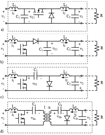
(24) SYNTHESIS OF POWER GYRATORS. L1 + v1. i1. -. L2 C1. + vC1. i2. + v2. C2. -. R. -. a). L1 + v1. L2. i1. + vC1. C1. -. i2. -. + v2. C2. R. -. b) C1. L1 + v1. i1. L2. -. +. -. i2 C2. vC1. v2 +. -. R. c) Ca. La + v1. i1. -. +. Cb. 1:n +. vCa. vCb. LO. -. i2 CO. v2. R. +. d). Fig. 2.6 Fourth order converters with non-pulsating input and output currents a) buck converter with input filter b) boost converter with output filter c) Cuk converter d) Cuk converter with galvanic isolation. The next step in our synthesis consists in the analysis in sliding-mode, under the constraints shown in Fig. 2.5, of each converter depicted in Fig. 2.6 except the Cuk converter with galvanic isolation whose complexity has deserved a complementary study within the frame of the research done in this thesis [30].. 2.2.1.1.1 Analysis of BIF converter as a power G-gyrators with variable switching frequency In the continuous conduction mode, the BIF converter has only one structural change during the switching period and therefore it can be represented by two piecewise-linear vector differential equations as follows. 10.
(25) SYNTHESIS OF POWER GYRATORS. x& = A1 x + B1. during TON. (2.8). x& = A2 x + B2. during TOFF. (2.9). where x = [ i1, i2, vC1, v2 ]+ is the state vector and matrices A1, B1, A2, B2 are given by A1 = . 0. 0. − 1. 0. 0. 1. 1. − 1. C1 0. 1. C1. C2. L1. L2 0. 0. 1 − L2 0 − 1 RC 2 0. V g L1 B1 = 0 0 0 . (2.10) A2 = . 0. 0. − 1. 0. 0. 0. −0. 0. 1. 0. 1. C1 0. C2. L1. 1 − L2 0 − 1 RC 2 0. V g L1 B2 = 0 0 0 . where it has been assumed v1=Vg. Equations (2.8) and (2.9) can be combined in only one bilinear expression X& = ( A1 X + B1 ) u + ( A2 X + B2 )(1 − u ). (2.11). where u=1 during TON and u=0 during TOFF Equation (2.11) can be expressed as follows X& = A2 X + B2 + ( A1 − A2 ) X u + (B1 − B2 ) u. (2.12). From (2.10) and (2.12), the following set of differential equations is derived: di1 − vC1 v g = + dt L1 L1 v di2 v = u C1 − 2 dt L2 L2 dvC1 i1 u = − i2 dt C1 C1 dvC 2 i v = 2 − 2 dt C 2 RC 2. 11. (2.13).
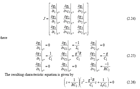
(26) SYNTHESIS OF POWER GYRATORS. Assuming S(x)=i2-gVg as sliding surface and imposing the invariance conditions [14] S(x)=0 dS and = 0 in (2.14) lead to the following expression of the equivalent control ueq(x) dt u eq ( x) =. v2 v C1. (2.14). Now, the discrete variable u is substituted by a continuous variable ueq(x) which can take all the values between 0 and 1. This variable ueq(x) represents the control law that describes the behaviour of the system restricted to the switching surface where the system motion takes place on the average. Therefore, ueq(x) is bounded by the minimum and maximum values of u. 0 < ueq ( x) < 1. (2.15). Substituting u by ueq(x) in (2.13) and taking into account the constraint i2=gVg imposed by the switching surface will result in the following ideal sliding dynamics: di1 − vC1 Vg = + = g1 ( x) dt L1 L1 dvC1 i1 v gVg = − 2 = g 2 ( x) dt C1 vC1 C1 dvC 2 gVg v = − 2 = g 3 ( x) dt C2 RC2. (2.16) (2.17) (2.18). The coordinates of the equilibrium point x* = [I1, I 2 , VC1,V2 ]+ are given by. [. x* = g 2 RVg , gVg , Vg , gVg R. ]. +. (2.19). Note that I1 = gV2. (2.20). I 2 = gVg. (2.21). Expressions (2.20) and (2.21) define the g-gyrator characteristics in steady-state. On the other hand, from (2.14) and (2.19), the expression of the equivalent control in the equilibrium point ueq(x*) results in ueq ( x*) = gR. (2.22). which is bounded by the minimum and maximum values of u. 0 < gR < 1. (2.23). The ideal sliding dynamics given by equations (2.16)-(2.18) is nonlinear. In order to study the stability of the system, equations (2.16)-(2.18) will be linearized around the equilibrium point x*. The corresponding Jacobian matrix J can be expressed as follows. 12.
(27) SYNTHESIS OF POWER GYRATORS. ∂g 1 ∂i1 ∂g J = 2 ∂i1 ∂g 3 ∂i1. x*. ∂g1 ∂vC1. x*. ∂g 2 ∂vC1. x*. ∂g3 ∂vC1. ∂g1 ∂v2. x*. ∂g 2 ∂v2. x*. ∂g3 ∂v2. x*. x* x* x* . (2.24). where ∂g1 ∂i1. =0 x*. ∂g1 ∂vC1. ∂g 2 ∂i1. 1 = C1 x*. ∂g 2 ∂vC1. ∂g3 ∂i1. ∂g3 ∂vC1. =0 x*. = x*. −1 L1. g 2R = C1 x* =0 x*. ∂g1 ∂v2 ∂g 2 ∂v2 ∂g3 ∂v2. =0 x*. =. −g C1. =. −1 RC2. x*. x*. (2.25). The resulting characteristic equation is given by 1 2 g 2 R 1 s − s + =0 s+ (2.26) C1 L1C1 RC2 which corresponds to an unstable system. The BIF regulator acting as a power gyrator can be stabilized by inserting a compensating network in the feedback loop using the technique reported in [38]. However, an important goal in our design is to minimize the complexity of the control loop, i.e., to reduce the loop to a multiplier, a linear algebraic circuit and a comparator that guarantee a sliding regime on the surface S(x) =i2-gVg . Thus, instead of feedback compensation, a damping network RdCd will be connected in parallel with capacitor C1 as shown in Fig. 2.7 [18]-[19].. Cd C1 Rd Fig. 2.7 Damping network connected in parallel with capacitor C1. It has to be pointed out that the damping network action is theoretically constrained to transient-state, keeping the converter steady-state equivalent circuit unchanged. The expression of the characteristic equation is given by 1 s + P( s ) = 0 RC2 where 1 1 1 g 2 R 2 1 g 2 R + − − P( s ) = s 3 + s + s+ R C L1C1Rd Cd d d Rd C1 C1 L1C1 Rd Cd C1 . 13. (2.27).
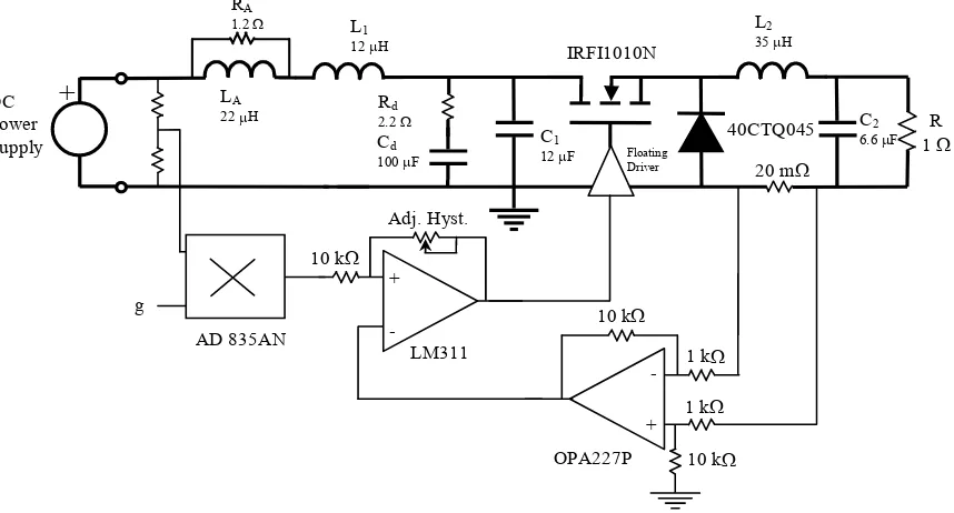
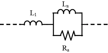
(28) SYNTHESIS OF POWER GYRATORS. In Appendix A, the Routh’s criterium is applied to the characteristic polynomial (2.27) leading to the following stability conditions Rd Cd <. C1 + Cd. (2.28). g 2R. Rd Cd > g 2 RL1. (2.29). g 2 RRd 2Cd 2 + g 2 RL1 (C1 + Cd ) < ( g 4 R 2 L1 + Cd ) Rd Cd. (2.30). Taking into account conditions (2.28)-(2.30), the block diagram depicted in Fig. 2.5 has been implemented as shown in Fig. 2.8 where the complete converter and its control circuit are depicted in detail. Note that the sliding surface is implemented by means of an analog multiplier and an operational amplifier-based linear circuit, while the ideal comparator function is performed by a hysteretic comparator. RA. 1.2 Ω. L2. L1. 12 µH. DC Power Supply. +. LA. 35 µH. IRFI1010N. Rd. 22 µH. 2.2 Ω. C1. Cd. 12 µF. 100 µF. 40CTQ045 Floating Driver. C2. 6.6 µF. R 1Ω. 20 mΩ. Adj. Hyst. 10 kΩ. +. g AD 835AN. 10 kΩ. LM311. + OPA227P. 1 kΩ 1 kΩ 10 kΩ. Fig. 2.8 Practical implementation of a BIF-converter-based G-gyrator L1 =12 µH, L2=35 µH C1=12 µF , C2=6.6 µF Cd=100 µF Rd=2.2 Ω, La=22 µH Ra=1.2 Ω, g=0.5 Ω -1 R=1 Ω. The parameters of the G-gyrator are given by the set of values Vg = 20 V, R = 1 Ω, g = 0.5 Ω -1, L1 = 12 µH, C1 = 12 µF, Cd = 100 µF, Rd = 2.2 Ω, L2 = 35 µH, and C2 = 6.6 µF. A damping network of type shown in Fig. 2.9, with La=22 µH and Ra=1.2 Ω, was also inserted to improve the dynamics behaviour of the gyrator state variables. 14.
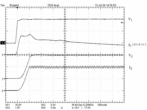
(29) SYNTHESIS OF POWER GYRATORS. La L1. Ra Fig. 2.9 Damping network connected in series with inductor L1. Figures 2.10-2.15 show the P-SPICE simulated responses and the corresponding experimental results of the BIF gyrator in different cases. Thus, Figs. 2.10 and 2.11 show respectively the simulated and experimental start-up of the power gyrator. Fig. 2.10. Simulated behaviour of the BIF converter-based G-gyrator with variable switching frequency during start-up. The measured power delivered to the load in steady-state is 101 W. Which corresponds to a 90 % efficiency. It can be verified in Figs, 2.10 and 2.11 that both circuits exhibit the G-gyrator characteristics defined in equations (2.1)-(2.2). Observe that output current I2 is 10 A for an input voltage of 20 V whereas input current I1 is 5 A for an output voltage of 10 V approximately. The effect of a pulsating voltage superposed to the nominal input voltage is illustrated in Fig 2.12 by simulation an in Fig. 2.13 by means of experimental results. The gyrator state variables reach a stable state after a transient-state produced by the insertion of step perturbations of ± 4 V in series with the input port. Note that in the two steady-states of Figs. 2.12-2.13, the output current is proportional to the input voltage, with a proportionality factor g=0.5 Ω -1.. 15.
(30) SYNTHESIS OF POWER GYRATORS. Fig. 2.11. Experimental behavior of the BIF converter-based G-gyrator with variable switching frequency during start-up. Fig. 2.12. Simulated behavior of the BIF converter-based G-gyrator in sliding-mode for a pulsating input voltage.. 16.
(31) SYNTHESIS OF POWER GYRATORS. Fig. 2.13. Experimental behavior of the BIF converter-based G-gyrator in sliding-mode for a pulsating input voltage.. The current source nature of the output current i2 is illustrated in Figs. 2.14-2.15 after introducing ± 50 % perturbations in the load resistance. The output voltage reproduces proportionality the pulsating behavior or the load, the proportionality constant being the output current i2 = 10 A.. Fig. 2.14. Simulated behaviour of the BIF converter-based G-gyrator in sliding-mode for a pulsating load. 17.
(32) SYNTHESIS OF POWER GYRATORS. Fig. 2.15. Experimental behavior of the BIF converter-based G-gyrator in sliding-mode for a pulsating load. We can conclude that in all cases under study (Figs. 2.10-2.15) the experimental results are in good agreement with the simulated predictions.. 2.2.1.1.2 Analysis of the BOF converter as a power G-gyrator with variable switching frequency A similar analysis of a boost with output filter (BOF) reveals that the equilibrium point is unstable. The corresponding characteristic equation is given by s − 1 s + 1 = 0 2 RC2 g L1R . (2.31). The insertion of the damping network shown in Fig. 2.7 cannot stabilize the system since the new characteristic equation still corresponds to an unstable system. This equation is expressed as 1 1 1 s + s + s − 2 RC2 Rd Cd L1 g R . = 0 . (2.32). It can be observed that the damping network RdCd only introduces a decoupled dynamic mode characterized by the time constant RdCd. As a consequence, there still remains an unstable mode created by the input current i1. In order to stabilize i1, a damping network is inserted in series with L1 as shown in Fig. 2.7. The resulting characteristic equation is given by 1 1 s + s + RC2 Rd Cd . . 2 s + s Ra + Ra − 1 − Ra = 0 2 L L g 2 RL L g RL 1 1 a 1 a . which still corresponds to an unstable system.. 18. (2.33).
(33) SYNTHESIS OF POWER GYRATORS. 2.2.1.1.3 Analysis of the Cuk converter as a power G-gyrator with variable switching frequency The sliding-mode analysis in the Cuk converter shows that the system is also unstable, the characteristic equation being 2 2 1 s + 1 = 0 s − g R 1 s + 1 + gR C1 L1C1 (1 + gR) RC2 . (2.34). The insertion of the damping network shown in Fig. 2.7 can stabilize the system, as demonstrated in Appendix B, if the following conditions are satisfied Rd Cd <. (C1 + Cd )(1 + gR ). (2.35). g 2R. Rd Cd > g 2 RL1. (2.36). g 2 RRd 2C d 2 + g 2 RL1 (C1 + C d )(1 + gR ) < ( g 4 R 2 L1 + C d (1 + gR )) Rd C d. (2.37). Using conditions (2.35)-(2.37), a Cuk converter-based power G-gyrator has been implemented as illustrated in Fig. 2.16 for the set of parameters Vg =20 V, R= 1Ω , g=0.5 Ω -1 L1 = 34 µH, C1 = 15 µF, Cd = 47 µF, Rd = 1.6 Ω, L2 = 25 µH and C2 = 6.6 µF. The damping network shown in Fig. 2.9 with La = 70 µH and Ra = 0.5 Ω has been also inserted in order to improve the dynamic response. Rd. Cd. 1.6 Ω. 47 µF. RA. 0.5 Ω. L1. DC Power Supply. +. L2. C1. 34 µH. 25 µH. 15 µF. LA. 70 µH. IRFI1010N. 40CTQ045. +. R 1Ω. Adj. Hyst.. g AD 835AN. 6.6 µF. 20 mΩ. Driver. 10 kΩ. C2. -. 10 kΩ LM311. OPA227P. + -. 1 kΩ 1 kΩ. 10 kΩ. Fig. 2.16. Practical implementation of the Cuk converter-based G-gyrator. Vg =20 V, R= 1Ω , g=0.5 Ω -1 L1 = 34 µH, C1 = 15 µF, Cd = 47 µF, Rd = 1.6 Ω, L2 = 25 µH, C2 = 6.6 µF, La = 70 µH and Ra = 0.5 Ω. 19.
(34) SYNTHESIS OF POWER GYRATORS. Figs. 2.17 and 2.18 illustrate respectively the PSPICE simulated behavior and the corresponding experimental results of the gyrator when a pulsating load is superposed to the nominal input voltage. The gyrator delivers 65 W at the output port with a 80 % efficiency. It can be observed that input perturbation is directly followed by the output current i2 and indirectly, through the converter action, by v2 and i1.. Fig. 2.17. Fig. 2.18. Simulated behavior of the Cuk converter-based G-gyrator in sliding-mode for a pulsating input voltage. Experimental behavior of the Cuk converter-based G-gyrator in sliding-mode for a pulsating input voltage.. 2.2.1.2 Power gyrator of type G with constant switching frequency The realization of a power gyrator operating at constant switching frequency will require the use of a pulse width modulation-based control (PWM). The direct search of a PWM control which guarantees a specific steady-state behavior is not simple. However, it was shown in [20]. 20.
(35) SYNTHESIS OF POWER GYRATORS. that the PWM nonlinear control that imposes S(x) = 0 in the steady-state in a switching regulator was the equivalent control ueq(x) found in the analysis of the switching regulator in sliding-mode with a slight modification which describes the regulator start-up until the surface S(x) is reached by the system trajectory. This correspondence between sliding-mode equivalent control and PWM zero-dynamics control is used in this section to derive PWM-based power G-gyrators. Fig. 2.19 shows a block diagram of a fourth-order PWM switching regulator with potential G-gyrator characteristics. It consists of a switching converter which is controlled by means of a PWM regulation loop whose duty cycle Г(x(t)) is a nonlinear function of the converter state variables. In the equilibrium point X* (steady-state), the duty cycle Г(x*) imposes I2 = g V1 which automatically implies I1 = g V2. Also, it has to be pointed out that TON (nT ) T. Γ( x(t )) t = nT =. (2.38). where T is the switching period, n is the nth period and TON(nT) is the duration of the on-state in the nth period. i2. i1. + v2. + v1. x=(i1, i2,…in, v1,v2,…vn). -. -. 1. u(t). 0. t T. +. -. vr(t) VM. Γ(x). 0. T. Fig. 2.19. Control Law. x. Block diagram of a PWM-based G-gyrator. Figure 2.20 illustrates equation (2.38). It can be observed that the continuous-time function Г(x) will be a good approximation of the discrete-time function is considerably smaller than the converter time-constants.. 21. TON (nT ) T. if the switching period.
(36) SYNTHESIS OF POWER GYRATORS. u(t) TON(T). TON(2T). TON(nT). T. nT. t. Γ(x(t)) Γ(x(t)). nT. T 2T. Fig. 2.20. t. Equivalence between Г(x(t)) and TON (nT ) at sampling instants. T. 2.2.1.2.1 Analysis of the BIF converter as PWM-based G-gyrator It has been shown in 2.2.1.1.1 that the insertion of the damping network of Fig. 2.7 in the BIF converter operating as G-gyrator with variable switching frequency can stabilize the system. The state equations of power stage are given by di1 − vC1 v g = + dt L1 L1 v di2 v = u C1 − 2 dt L2 L2 dvC1 i1 vCD − vC1 i2 = + − u dt C1 RD C1 C1. (2.39). dvCD v v = C1 − CD dt RD C D RD C D dv2 i2 v = − 2 dt C2 RC2. where u=1 during TON and u=0 during TOFF. Under the above mentioned conditions of a switching frequency considerably bigger than the converter natural frequencies, the discrete variable u in (2.39) can be substituted by a continuous variable Г(x(t)) which takes the average value of u in each period at the corresponding sampling instants T, 2T, … nT as expressed in (2.38) and as shown in Fig. 2.20. Note that Г(x(t)) can take all the values between 0 and 1 and therefore is bounded by the maximum and minimum values of u 0 < Γ( x(t )) < 1 Now, we can write the equation describing the dynamics of i2 as follows. 22. (2.40).
(37) SYNTHESIS OF POWER GYRATORS. v di2 v = Γ C1 − 2 dt L2 L2. (2.41). If equation (2.41) could be expressed as. (. di2 RK = gVg − i2 dt L2. ). (2.42). equation (2.42) would result in steady-state in. I 2 = gVg. (2.43). which is the desired behavior of a G-gyrator. Equation (2.41) will become equation (2.42) if Г(x(t)) is expressed as. Γ( x) =. (. v2 + RK gVg − i2. ). vC1. (2.44). which in the steady-state becomes. Γ( x*) =. v2 vC1. (2.45). which is the equivalent control corresponding to the sliding-mode approach when the constraint S(x) = i2- gVg is added to (2.39). Therefore, the dynamics of the system can be separated in two types of dynamics, i.e., the L dynamics of the start-up given by the time-constant 2 and the dynamics of the system RK restricted to the surface S(x) = i2- gVg where the system motion takes place on the average. The last dynamics is exactly equal to the ideal sliding dynamics analyzed in 2.2.1.1.1. Hence, the characteristic polynomial DPWM(s) will be expressed as R DPWM ( s ) = DSLIDING ( s ) s + K L2 . (2.46). where DSLIDING(s) is the characteristic polynomial found in 2.2.1.1.1 describing the ideal sliding dynamics. Hence, the system characteristic equation DPWM(s) = 0 will be given by 1 R P( s) = 0 s + K s + L2 RC2 1 1 1 g 2 R 2 1 g 2 R + − − P( s ) = s 3 + s + s+ R C C1 L1C1Rd Cd d d Rd C1 L1C1 Rd Cd C1 . (2.47). Therefore, the system will be stable if conditions (2.28)-(2.30) found previously in the analysis of the G-gyrator with variable switching frequency are also satisfied.. 23.
(38) SYNTHESIS OF POWER GYRATORS. Figure 2.21 illustrates the practical implementation of the block diagram depicted in Fig. 2.19. The converter parameters satisfy conditions (2.28)-(2.30) and are given by Vg = 20 V, R = 1 Ω, g = 0.5 Ω -1, L1 = 12 µH, C1 = 12 µF, Cd = 100 µF, Rd = 2.2 Ω, RK= 48 Ω, L2 = 35 µH, C2 = 6.6 µF. The switching frequency fs is 200 kHz. Note that a damping network of the type shown in Fig, 2.9 with La=22 µH and Ra=1.2 Ω was also inserted to improve the dynamic behavior of the gyrator state variables. Figures 2.22-2.27 show the P-SPICE simulated responses and the corresponding experimental results of the PWM-BIF G-gyrator in different cases. Figures 2.22 and 2.23, in particular, illustrate respectively the simulated and experimental start-up of the G-gyrator. The measured power delivered to the load in steady-state is 102 W, this implying a 88 % efficiency. It can be verified in both figures that the circuit exhibits the gyrator characteristics defined in equations (2.1)-(2.2).. io. La L1. i1. Vg. L2. IRFI1010N. VC1. +. i2. Rd. Ra C1. D. C2. Cd. R. V2S. -. 20mO 3k. v2. 3k 11k. gVg g. AD835. 3524. 11k OPA277. VC1 10k. 10k. AD538. 40k 1k OPA277. 10k. OPA277. OPA277 10k. 10k. V2S 10k. gVg. 1k 40k. 2k VC1. Practical implementation of a BIF converter-based PWM G-gyrator. Vg = 20 V, R = 1 Ω, g = 0.5 Ω , L1 = 12 µH, C1 = 12 µF, Cd = 100 µF, Rd = 2.2 Ω, RK= 48 Ω, L2 = 35 µH, C2 = 6.6 µF, fs = 200 kHz, La=22 µH and Ra=1.2 Ω. Fig. 2.21. -1. The effect of a pulsating voltage superposed on the nominal input voltage is illustrated in Fig. 2.24 by simulation and in Fig. 2.25 by means of experimental results. It can be observed that the gyrator state variables reach a stable state after a transient-state produced by the insertion of step perturbations of ± 4 V in series with the input port. Note that in the two steady-states of Figs. 2.24 and 2.25 the output current is proportional to the input voltage with a proportionality factor g = 0.5 Ω -1.. 24.
(39) SYNTHESIS OF POWER GYRATORS. vC1 vg. i2 v2. Fig. 2.22. i1. Simulated behavior of the PWM BIF converter-based G-gyrator during start-up. v1. i1 (0.1 A/V) v2 i2. Fig. 2.23. Experimental behavior of the PWM BIF converter-based G-gyrator during start-up. 25.
(40) SYNTHESIS OF POWER GYRATORS. vg. vC1. i2. v2. i1. Fig. 2.24. Simulated behavior of the PWM BIF converter-based G-gyrator for a pulsating input voltage. The current source nature of the output current i2 is illustrated in Figures 2.26 (simulation) and 2.27 (experiments) after introducing ± 50 % perturbation in the load resistance. The output voltage is proportional to the pulsating load, the proportionality constant being the output current i2 = 10 A.. i2 v1. i1 (0.1 A/V) v2. Fig. 2.25. Experimental behavior of the PWM BIF converter-based G-gyrator for a pulsating input voltage. 26.
(41) SYNTHESIS OF POWER GYRATORS. vC1 vg. i2 v2 i1. Fig. 2.26. Simulated behavior of the PWM BIF converter-based G-gyrator for a pulsating load. v1 i2 i1 (0.1 A/V). v2. Fig. 2.27. Experimental behavior of the PWM BIF converter-based G-gyrator for a pulsating load. In all the cases depicted in Fig. 2.22-2.27 there is a good agreement between simulated and experimental results. We have to point out that the switching frequency is constant in the whole operation regime, i.e., in both transient and steady-states.. 27.
(42) SYNTHESIS OF POWER GYRATORS. 2.2.1.3 Other types of G-gyrators Equations (2.1)-(2.2) define a power gyrator of type G which is intended to transform a voltage source at the input port into a current source at the output port. However, we would synthesize a G-gyrator intending to transform a voltage source at the output port into a current source at the input port. In such situation, the power gyrator could be implemented as illustrated in Fig. 2.27 where a 4th order converter is also assumed in the power stage.. DC-TO-DC SWITCHING CONVERTER i2. i1. + v2. + v1. -. u(t). 1 0. 1. t. u 0 S(x). S(x)=i1-gv2 1. Fig. 2.28. Σ-g. Block diagram of a dc-to-dc switching regulator operating in sliding-mode with G-gyrator characteristics and with i1 as controlled variable.. Since the regulator establishes the gyrator characteristics through the control of current i1, we will call this class of circuits G-gyrators with controlled input current. The fourth order converters previously studied, i.e., BIF, BOF and Cuk converter will be analyzed next in sliding-mode operation assuming S(x) = i1 - gv2, where v2 is a constant voltage.. 28.
(43) SYNTHESIS OF POWER GYRATORS. 2.2.1.3.1 Analysis of the BIF converter as G-gyrator with controlled input current and variable switching frequency The set of equations describing the BIF converter are the following di1 − vC1 Vg = + dt L1 L1 di2 vC1 V u− 2 = dt L2 L2. (2.48). dvC1 i1 i2 = − u dt C1 C1. where V2 is a constant voltage. Considering S(x) = i1 - gv2 as sliding surface and imposing the invariance conditions S(x) = dS 0 and = 0 reveals that there is no equivalent control and hence no sliding motions can be dt induced in the switching converter. However, it has been found by simulation that the system has a stable limit cycle if the comparator shown in Fig. 2.28 is a hysteretic comparator. Fig. 2.29 shows the PSIM simulations of a BIF converter-based G-gyrator with controlled input current during start-up for the set of parameters Vg = 20 V, V2 = 12 V, g = 0.5 Ω -1, L1 = 12 µH, C1 = 12 µF, Cd = 100 µF, Rd = 2.2 Ω, L2 = 35 µH, La=22 µH and Ra=1.2 Ω.. vC1. v2 i2. Fig. 2.29. Simulated behavior of a BIF converter-based G-gyrator with controlled input current during startup. Also figure 2.30 illustrates the PSIM simulations of the gyrator behavior for a pulsating input voltage.. 29.
(44) SYNTHESIS OF POWER GYRATORS. vC1 vg. v2 i2. Fig. 2.30. Simulated behavior of a BIF converter-based G-gyrator with controlled input current for a pulsating input voltage. It has to be pointed out that in both figures the circuit exhibits stable G-gyrator characteristics.. 2.2.1.3.2 Analysis of the Cuk converter as G-gyrator with controlled input current and variable switching frequency The equations describing the Cuk converter are in this case Vg di1 − vC1 vC1 = + u+ dt L1 L1 L1 V di2 vC1 = u− 2 L2 dt L2. (2.49). dvC1 i1 i i = − 1 u− 2 u dt C1 C1 C1 where V2 is a constant voltage. Assuming S(x) = gv2- i1 as a describing surface and imposing the invariance conditions dS S(x)=0 and = 0 in (2.49) leads to the equivalent control dt ueq ( x) =. vC1 − Vg vC1. (2.50). Introducing (2.50) in (2.49) and assuming S(x)=0 result in the following ideal sliding dynamics. 30.
(45) SYNTHESIS OF POWER GYRATORS. di2 vC1 − V g V2 = − = g1 ( x) dt L2 L2. (2.51). dvC1 gV2 gV2 vC1 − V g i2 vC1 − V g = − − = g 2 ( x) dt C1 C1 vC1 C1 vC1. (2.52). The coordinates of the equilibrium point of the ideal sliding dynamics are. [. x* = [I1, I 2 ,VC1 ]+ = gV2 , gVg ,V2 + Vg. ]+. (2.53). where it can be observed that I1 = gV2 and I2 = gVg which corresponds to a steady-state gyrator behavior. The linearization of equation (2.51) around the equilibrium point (2.52) yields the Jacobian matrix ∂g1 ∂i2 x * J = ∂g 2 ∂i2 x *. ∂g1 0 ∂vC1 x * = − 1 V2 ∂g 2 ∂vC1 x * C1 V2 + V g. . C1 (V2 + V g ) . 1 L2 − gVg. (2.54). Hence, the characteristic equation is given by s2 + s. gVg C1 (V2 + V g ). +. V2 1 =0 L2 C1 (V2 + V g ). (2.55). which corresponds to a stable system. Figs. 2.31-2.34 show the PSIM simulations of a Cuk converter-based G-gyrator with controlled input current with the set of parameters Vg=15 V, L1 = 75µH, C1 = 10 µF, L2 = 75 µΗ, g = 0.5 Ω-1 ,V2 = 24 V and 12 V. The G-gyrator characteristics are clearly illustrated in all the cases simulated in Figs. 2.31-2.34. 31.
(46) SYNTHESIS OF POWER GYRATORS. Vg. i1. v2 i2. Fig. 2.31. Simulated behavior of a Cuk converter-based G-gyrator with controlled input current during startup (V2=12 V). Vg. i1. v2 i2. Fig. 2.32. Simulated response of a Cuk converter-based G-gyrator with controlled input current for a pulsating input voltage (V2=12 V). 32.
(47) SYNTHESIS OF POWER GYRATORS. Vg i1. v2 i2. Fig. 2.33. Simulated behavior of a Cuk converter-based G-gyrator with controlled input current during start-up (V2=24 V). Vg i1. v2 i2. Fig. 2.34. Simulated behavior of a Cuk converter-based G-gyrator with controlled input current for a pulsating input voltage (V2=24 V). The Cuk converter-based power G-gyrator with controlled input current has been implemented as illustrated in Fig. 2.35 for the set of parameters Vg =15 V, L1 = 75µH, C1 = 10 µF, L2 = 75 µΗ, g = 0.25 Ω-1 (0.5 Ω-1),VBAT = 24 V ( 12V).. 33.
(48) SYNTHESIS OF POWER GYRATORS. C1. L1. i2. i1. Vg. L2. IRFI1010N. D. C2. V2. 20mO Adj. Hyst. 3k. 3k 10k 11k. 11k. Fig. 2.35. OPA277. LM311. -g. AD835. Practical implementation of the Cuk converter-based G-gyrator with controlled input current. Vg=15 V, L1 = 75µH, C1 = 10 µF, L2 = 75 µΗ, g = 0.25 Ω-1 (0.5 Ω-1) ,VBAT = 24 V ( 12V).. Figures 2.36 and 2.37 show the experimental behavior of the gyrator during start-up for V2 = 12 V and V2 = 24 V respectively. The gyrator response to ± 4 V input voltage perturbations of step type is illustrated in Figs. 2.38 and 2.39 for V2 = 12 V and V2 = 24 V respectively. The experimental results are in good agreement with the simulations previously shown. The gyrator delivers to the 12 V battery 75 W with a 82 % efficiency and the same power to the 24 V battery with 83 % efficiency.. v1. i1 (0.1 A/V). i2 v2. Fig. 2.36. Experimental behavior of a Cuk converter-based G-gyrator with controlled input current during start-up ( V2=12 V ). 34.
(49) SYNTHESIS OF POWER GYRATORS. v1 i1 (0.1 A/V). i2 v2. Fig. 2.37. Experimental behavior of a Cuk converter-based G-gyrator with controlled input current during start-up (V2=24 V). v1 i1 (0.1 A/V). i2. v2. Fig. 2.38. Experimental response of a Cuk converter-based G-gyrator with controlled input current to a pulsating input voltage (V2=12 V). 35.
(50) SYNTHESIS OF POWER GYRATORS. v1. i1 (0.1 A/V). i2 v2. Fig. 2.39. Experimental response of a Cuk converter-based G-gyrator with controlled input current to a pulsating input voltage (V2=24 V). 2.2.1.3.3 Analysis of the BOF converter as G-gyrator with controlled input current and variable switching frequency The BOF converter can be represented by the following set of differential equations Vg di1 vC1 = (u − 1) + L1 dt L1 di2 vC1 V2 = − dt L2 L2. (2.55). dvC1 i1 i i = − 1 u− 2 C1 dt C1 C1 where V2 is a constant voltage Assuming S(x) = gV2-i1 as a switching surface and imposing the invariance conditions dS = 0 in (2.55) results in the equivalent control S(x) = 0 and dt ueq ( x) =. vC1 − Vg vC1. 36. (2.56).
(51) SYNTHESIS OF POWER GYRATORS. The introduction of (2.56) in (2.55) leads to the following ideal sliding dynamics di2 vC1 V2 = − = g1 ( x) dt L2 L2 dvC1 gV2 gV2 vC1 − Vg i2 = − − = g 2 ( x) (2.57) dt C1 C1 vC1 C1 The coordinates of the equilibrium point are x* = [I1, I 2 ,VC1 ]+ = gV2 , gVg ,V2 + Vg + (2.58). [. ]. where it can be observed that I1 = gV2 and I2= gVg , this representing the steady-state gyrator equations. Linearizing (2.57) around the equilibrium point (2.58) yields the Jacobian matrix ∂g1 ∂i2 J = ∂g 2 ∂i2. x*. x*. 0 x* = ∂g 2 − 1 ∂vC1 x* C1 ∂g1 ∂vC1. 1 L2 − gVg C1V2 . (2.59). Finally, the characteristic equation corresponding to (2.59) is given by s2 + s. gVg C1V2. +. 1 =0 L2C1. (2.60). which represents a stable system. Figs. 2.40 and 2.41 illustrates by means of PSIM simulation the BOF behavior as a Ggyrator with controlled input current for the set of parameters Vg=15 V, g = 0.5 Ω-1, L1 = 50µH, C1 = 10 µF, L2 = 65 µΗ, V2 = 24 V. Fig. 2.40 shows the power gyrator start-up while Fig. 2.41 depicts the gyrator response to a pulsating input voltage.. vC1 Vg. Fig. 2.40. Simulated behavior of a BOF converter-based G-gyrator with controlled input current during start-up (V2=24 V). 37.
(52) SYNTHESIS OF POWER GYRATORS. vC1 Vg. v2 i2. Fig. 2.41. Simulated behavior of a BOF converter-based G-gyrator with controlled input current for a pulsating input voltage (V2=24 V). 2.2.2 Power gyrator of type R The synthesis goal of a power R-gyrator is designing a switching structure characterized by the following steady-state equations V1 = rI 2. (2.61). V2 = rI1. (2.62). where r is the gyrator resistance. As stated previously, switching structures used in the design of power gyrators are not versatile, i.e., a G-gyrator cannot be adapted to perform R-gyrator functions. It has to be pointed out that a current source at the input port of the circuit depicted in Fig. 2.5 is not compatible with the series inductor and therefore such circuit cannot be used for the current-voltage transformation. Hence, the block diagram of a power R-gyrator can be represented as shown in Fig. 2.42 where ig is the input current source to be transformed into an output voltage source by means of the gyrator action. It can be observed that S(x) = 0 in steady-state, i.e., V2 = rIg which implies V1 = rI2.. 38.
(53) SYNTHESIS OF POWER GYRATORS. i2 + v2. IG. u(t). 1 0. 1. t. u 0 S(x). S(x)=v2-rIg -r. Fig. 2.42. Σ1. Block diagram of a dc-to-dc switching regulator operating in sliding-mode with R-gyrator characteristics.. The most simple converters with the topological constraints depicted in the block diagram of Fig. 2.42 are shown in Fig. 2.43. Such converters are derived by slight modification of the BOF converter, Cuk converter and Cuk converter with galvanic isolation. Note that series connection of a voltage source and an inductor at the input port of the BOF and Cuk converters depicted in Fig. 2.6 has been substituted by a current source, this implying a dynamic order reduction to a third-order system. L2 IG. + vC1. C1. i2. -. + v2. C2. R. -. a) C1. L2. -. + IG. -. i2 C2. vC1. R. v2 +. b) Ca. -. + IG. Cb. 1:n +. vCa. vCb. LO. -. i2 CO. v2. R. + c). Fig. 2.43. Current to voltage dc-to-dc switching converters with non-pulsating input and output currents a) boost converter with output filter b) Čuk converter c) Čuk converter with galvanic isolation. 39.
Figure


+7
![Fig. 1 is ideal and therefore is a POPI structure. Note that imposing a sliding-mode regime to the output current requires i2 to be a continuous function of time [13], which implies the existence of a series inductor at the output port](https://thumb-us.123doks.com/thumbv2/123dok_es/5263641.96654/23.595.150.449.192.527/structure-imposing-current-requires-continuous-function-existence-inductor.webp)
Documento similar
Firstly, considering CPVMatch module specifications, number of modules in the system and potential mismatching sources, a buck converter has been determined as the
Una vez que se tienen estos datos se procede a realizar un dataframe, llamado converter, que contiene como se encuentra clasificado el paciente originalmente, la clasificación
Flyback converters and related methods are provided. In one implementation, an on-time of a flyback converter low side switch is maintained substantially at a resonant half resonance
ADC is the analog to digital converter, and Gvc(z) is the controller that takes into account the mean value of the output voltage, which in our case generates k, that is
The authors would like to thank the students whose excel- lent work and whose comments have helped improve the exper- iments carried out at the Power Electronics Laboratory of
For a multiphase active clamp buck converter, with the same deviation in the components, it can be proved that there is a better current sharing among phases than in a converter
To test the current sharing due to the high output im- pedance, a three-phase ZVS active clamp buck converter was implemented. IRF540 and MBR1045 are used as switching devices
For instance, if the desired filter specifications can be satisfied with a fourth-order filter with two transmission zeros, by using our concept it would be necessary to implement
