Non linear absorption of InN/InGaN multiple quantum well structures at optical telecommunication wavelengths
15
0
0
Texto completo
(2) Non-linear absorption of InN/InGaN multiple-quantum-well structures at optical telecommunication wavelengths. F. B. Naranjo1, P. K. Kandaswamy2, S. Valdueza-Felip1, V. Calvo2, M. GonzálezHerráez1, S. Martín-López3, P. Corredera3, J. A. Méndez3, G. R. Mutta4, B. Lacroix4, P. Ruterana4 and E. Monroy2. 1. Grupo de Ingeniería Fotónica, Departamento de Electrónica, Universidad de Alcalá Campus Universitario, 28871 Alcalá de Henares, Madrid, Spain.. 2. CEA-Grenoble, INAC / SP2M, 17 rue des Martyrs, 38054 Grenoble cedex 9, France. 3. Instituto de Óptica, (CSIC), c/ Serrano 144, 28006 Madrid, Spain. 4. CIMAP, ENSICAEN 6, Bld Maréchal Juin 14050 Caen France. Abstract. We report on the nonlinear optical absorption of InN/InxGa1-xN (x = 0.8, 0.9) multiple-quantum-well structures characterized at 1.55 μm by the Z-scan method in order to obtain the effective nonlinear absorption coefficient (α2) of the samples at high repetition rate. Saturable absorption is observed for the sample with x = 0.9, with an effective α2 ~ -9x103 cm/GW for the studied optical regime. For lower In content in the barrier, reverse saturable absorption is observed, which is attributed to two-photon absorption.. a) E-mail: [email protected].
(3) State-of-the-art electronic switching networks are approaching their bandwidth limit due to capacitive charging. Further development of optical networks requires evolving towards an all-optical approach, in order to fully exploit the immense bandwidth supported by wavelength-division multiplexing (WDM). All-optical signal processing requires new optical devices for ultrafast signal managing. Resonant optical nonlinearities in semiconductors emerge as a feasible approach for the development of these devices [1]. In particular, low-dimensional semiconductor structures can attain the required specifications thanks to the enhancement of the third-order optical susceptibility. Recently, III-Nitride semiconductors have attracted much attention for telecom applications in the C band (1530 to 1565 nm). Optical switching based on intersubband transitions in GaN/AlN nanostructures operating at 1.5 μm has been reported [2][3]. These structures display ultra-fast carrier relaxation time due to the strong electronphonon interaction in these materials [3][4]. III-nitride materials can also access the telecommunication spectral range with interband transitions, using InN-based technology. The development of InN growth by molecular-beam epitaxy (MBE) has led to high-quality material with a band gap close to 0.65 eV at room temperature [5]. This semiconductor shows recovery times in the range of ps [6], and displays saturable absorption (SA) and close-to-resonant behavior at 1.55 μm wavelength [7]. InN-based multiple-quantum-well (MQW) should present enhanced nonlinear behavior and the possibility of tuning the resonance wavelength within the optical fiber transparency band. In this work we present the nonlinear optical characterization of InN/InGaN MQW structures, in order to assess their feasibility for applications in all optical-based devices operating at 1.55 μm.. 2.
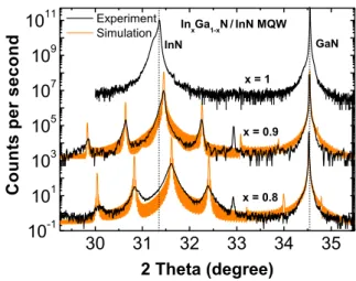
(4) MQW structures consisting of 41 periods of 4.5 nm InN wells and 7 nm InxGa1xN. barriers with x = 0.8 and 0.9 were grown by plasma-assisted MBE on 10-µm-thick. GaN-on-sapphire templates. The structures were grown at 450ºC, with a N-limited growth rate of 280 nm/h. A reference 1-μm-thick InN layer was grown under the same conditions. The optical and structural properties of InN thin films have been reported in ref. 8. Due to the 11% lattice mismatch, InN layers deposited on GaN contain the usual misfit defects that form inside nitride layers [9]. However, it has been noticed a particularly low density of basal stacking faults formed at the initial stages of the InN epitaxy [8]. It is worth saying that such defects and their interaction contribute to reduce the threading dislocation density in GaN layers [10]. Therefore, throughout the InN layer thickness, edge-type threading dislocations keep a uniform density in the range of mid 109 cm-2 [8]. It must be pointed out that GaN-based waveguide devices with similar density of threading dislocations have been reported [2],[3]. The structural quality of the MQW samples was assessed by high-resolution xray diffraction (HRXRD), transmission electron microscopy (TEM) and atomic force microscopy (AFM). Figure 1 displays the ω−2θ scan of the (0002) x-ray reflection of the MQWs compared to theoretical calculations. The several satellites of the superlattice reflection confirm the good periodicity, while the angular shift is consistent with the expected In mole fraction. Regarding the TEM analysis, conventional imaging of InxGaN1-x/InN is not useful for x compositions close to 1, since the atomic number difference is not enough to provide good contrast. However, it was noticed that due to the rapid changes in lattice parameters, the distance between the 0002 InN and InGaN beam positions in the diffraction pattern increases substantially and this has been exploited for asymmetric dark-field image formation, which uses mainly one of the. 3.
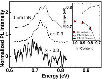
(5) beams. Depending on the contributing beam (InN or InGaN), either the well or the barrier is imaged in dark, whereas the other is bright. Figure 2(a) shows such an asymmetric dark-field TEM image of the MQW sample with x=0.9. As attested by the inserted intensity profile (InGaN bright), we have a good uniformity of the well and barrier thickness, in agreement of those estimated by HRXRD. Root-mean-square (rms) surface roughness below 1 nm were measured by AFM in 2×2 μm2 surface for all the structures, as it is shown in Fig. 2(b) for the MQW structure with x=0.9. Linear optical characterization was performed using low-temperature (T = 5 K) photoluminescence (PL) measurements with an Ar laser (λ = 514 nm) as excitation source. Normalized PL spectra of the InN/InxGa1-xN MQWs and the InN reference sample are shown in Fig. 3. The infrared (IR) emission energy of the samples red shifts when decreasing the In content in the barrier. For the sample with x ~ 0.9 the IR emission is enhanced, with a full width at half maximum (FWHM) as narrow as 44 meV. On the other hand, the peak emission intensity decreases for the sample with x ~ 0.8. These results can be explained in terms of the huge piezoelectric fields that can be expected in this kind of structures [11]. The band diagram of these samples was calculated using the Nextnano3 Schrödinger-Poisson solver [12]. The inset of Fig. 3 shows the simulation results when considering the MQW structures either relaxed or fully strained on InN. The experimental PL emission energy undergoes the red shift expected in the case of MQWs fully strained on InN. Nonlinear absorption coefficient, α2 was obtained through Z-scan measurements. [13]. The Z-scan setup is equipped with a 100 fs-pulse width fiber-laser source with a repetition rate of 100 MHz. During Z-scan measurements, the sample is moved along the optical axis of the focused laser beam (Z axis direction), while the transmittance of. 4.
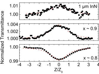
(6) the sample is recorded as a function of the z position. The measurements to obtain α2 were performed in open aperture configuration using a 5 cm focal-length achromatic lens for focusing the laser beam. With this system configuration, a beam waist ω0 ~ 10 µm is obtained, leading to a Rayleigh range z0 ~ 200 µm. Measurements were performed at power levels below 0.8 GW/cm2, the minimum power at which a measurable response is obtained from the GaN-template substrate. The experimental results were analyzed considering the relationship between the time-integrated transmission, Topt, and the non linear absorption given by [13] Topt = 1 −. 1. α 2 I 0 Leff. 2 2. 1 + ⎛⎜ z ⎞⎟ ⎝ z0 ⎠. 2. (1). where I0 is the maximum input power, Leff = (1 − e −α 0 L ) / α 0 is the effective length of the sample, α0 and L are the linear absorption coefficient and the thickness of the sample, respectively, and z is its on-axis position, z=0 being the focal plane of the lens. The values of α0 were estimated at 1.55 µm wavelength from transmission measurements. For analyzed MQW samples, with α0~3•102 cm-1, the effective length obtained is the total active length of the QWs. A value of α0 = 4±0.4•103 cm-1 was estimated for the InN thick sample, leading to a Leff = 825±25 nm. Thus, the error in the estimation of α2 due to Leff error is below 5%. Figure 4 shows the Z-scan results obtained for the 1-µm-thick InN reference sample and the analyzed InN /InxGa1-xN MQW samples, together with the fitting of the experimental results to eq. 1. The InN sample presents SA behavior with α2 = -1450 cm/GW, which corresponds to a saturation intensity of Isat~1.4 GW/cm2. This SA effect is attributed to band filling [7], and can be explained in terms of the low effective mass of InN [14].. 5.
(7) The superlattice with x ~ 0.9 shows SA with α2 = -9150 cm/GW. The increase of the SA coefficient compared to bulk InN is attributed to quantization effects which reduce the density of states at the band edge, and it leads to a reduction in Isat down to 16 MW/cm2. Indeed, simulations performed for this structure taking into account the carrier density photogenerated during the Z-scan measurements (up to 1.7 × 1012 cm-2) show that the carrier screening of the internal electric field cannot justify the change in the transmission observed. Results obtained from the sample with x ~ 0.8 points to a reverse saturable absorption (RSA) behavior with a value of α2 = +3650 cm/GW. For this sample the excitation energy is far from the estimated recombination energy between levels of confined carriers in the wells. Thus, the RSA is attributed to two-photon absorption (TPA) from carriers confined in the H1 level to the continuum. This effect has already been observed in AlGaAs/GaAs MQW structures [15]. The obtained values of α2 could be affected by the high repetition rate of the laser source, which produces local thermal effects in the sample during the measurements. Due to these thermal effects, the sample behaves as an optical lens, which might lead to an overestimation of nonlinear parameters obtained by the Z-scan method. With our measurements conditions and considering a thermal diffusion coefficient of D ~ 0.55 cm2/s for InN [16] these thermal effects could affect to the measurements for laser repetition rates above ~1 MHz [17]. However, it must be pointed out that the obtained nonlinear absorption corresponds to the expected behavior of the analyzed samples in a telecommunication application under high repetition rates. In conclusion, we have studied the nonlinear optical absorption of InN/InxGa1-xN superlattices with high In content in the barriers, operating in the telecommunication regime. The optical properties of the structures are determined by the huge piezoelectric. 6.
(8) field present in the wells. SA is observed for the sample with x ~ 0.9, with an enhancement of nonlinear absorption compared to bulk InN. On the other hand, RSA attributed to two-photon absorption is obtained for the sample with x ~ 0.8. These results open the possibility to control and enhance the nonlinear properties of InN-based superlattices with a view to their application to all-optical telecommunication networks.. Authors would like to acknowledge Dr. S. Fernández, for useful discussions. Partial financial support was provided by Spanish government projects TEC2009-14423-C0202, and by Comunidad de Madrid, Project S2009/ESP-1781.. 7.
(9) References [1] O. Wada, New J. Phys. 6, 183 (2004). [2] Y. Li, A. Bhattacharyya, C. Thomidis, T. D. Moustakas, R. Paiella, J. Appl. Phys. 104 083101 (2008). [3] N. Iizuka, K. Kaneko, and N. Suzuki J. Appl. Phys. 99, 093107 (2006). [4] S. Valdueza-Felip, F. B. Naranjo, M. González-Herráez, H. Fernández, J. Solis, F. Guillot, E. Monroy, L. Nevou, M. Tchernycheva, and F. H. Julien, IEEE. Photonics Tech. Lett. 20 (16), 1366 (2008). [5] V. Y. Davydov, A. A. Klochikhin, R. P. Seisyan, V. V. Emtsev, S. V. Ivanov, F. Bechstedt, J. Furthmuller, H. Harima, V. Mudryi, J. Aderhold, O. Semchinova, and J. Graul, Phys. Stat. Sol. B 229, R1 (2002). [6] F. B. Naranjo, M. González-Herráez, H. Fernández, J. Solis, and E. Monroy, Appl. Phys. Lett. 90, 091903 (2007). [7] F. Chen, A. N. Cartwright, H. Lu, and J. Schaff, Appl. Phys. Lett. 83, 4984 (2003). [8] P. Ruterana, A.L. Syrkin, E. Monroy, E. Valcheva and K. Kirilov, Phys. Stat. Sol. (c) 7, 1301 (2010). [9] P. Ruterana, V. Potin, B. Barbaray, and G. Nouet, Phil. Mag. A 80, 937 (2000). [10] V. Potin, P. Ruterana and G. Nouet, J. Phys. Condensed Matter 12, 10301(2000). [11] Md. T. Hasan, A. G. Bhuiyan, and A. Yamamoto, Solid State Electron. 52, 134 (2008). [12] S. Birner, T. Zibold, T. Andlauer, T. Kubis, M. Sabathil, A. Trellakis, and P. Vogl, IEEE Trans. Electron Devices 54, 2137 (2007) [13] M. Sheik-Bahae, A. A. Said, T._H. Wei, D.J. Hagan, and E. W. Van Stryland IEEE J. Quantum. Electron. 26, 760 (1990). 8.
(10) [14] I. Gorczyca, J. Plesiewicz, L. Dmowski, T. Suski, N. E. Christensen, A. Svane, C. S. Gallinat, G. Koblmueller, and J. S. Speck, J. Appl. Phys. 104, 013704 (2008) [15] J. U. Kanga, J. B. Khurgin, C. C. Yang, H. H. Lin, G. I. Stegeman, Appl. Phys. Lett. 73, 3638 (1998). [16] P.-C. Wei, H.-C. Shih, S . Chattopadhyay, C.-M. Hsu, F.-S. Lin, K.-H. Chen, A. Ganguly, L.-C. Chen J. Appl. Phys. 104, 064920 (2008). [17] R. Nalda, R. Coso, J. Requejo-Isidro, J. Olivares, A. Suarez-Garcia, J. Solis, C. N. Afonso, J. Opt. Soc. Am. B 19, 289 (2002).. 9.
(11) Figure captions. Figure 1. HRXRD ω−2θ scan of the (0002) x-ray reflection of the InN reference sample and the InN/InGaN MQW structures, compared to theoretical calculations using the X’Pert Epitaxy 40 software from Phillips Analytical. Measurements are vertically shifted for clarity.. Figure 2. (a) Dark field (g = 0002) TEM micrograph of the InN/InxGa1-xN MQW sample with x~0.9. In the inserted profile along c, the QWs are well delineated. (b) AFM image of the same sample exhibiting atomic steps.. Figure 3.. Low temperature (T = 5 K) PL spectra of the analyzed samples. Inset:. Recombination energies as a function of In content in the barriers obtained from electronic simulations considering the structure fully relaxed (open squares), fully strained on InN (solid squares), and experimental PL peak energy (solid circles).. Figure 4. Z-scan measurements of InN sample and InN/InxGa1-xN samples with x ∼0.9 and x∼ 0.8. The fitting to the eq. (1) is also shown for each case.. 10.
(12) Figure 1. 11. Counts per second. 10. Experiment Simulation. 9. 10. InxGa1-xN / InN MQW GaN. InN. x=1. 7. 10. 5. 10. x = 0.9. 3. 10. 1. 10. x = 0.8. -1. 10. 30. 31 32 33 34 2 Theta (degree). 35.
(13) Figure 2. Surface. Interface.
(14) 2. Energy (eV). Normalized PL Intensity. Figure 3. 1 Pm InN. 0.8. 0.7. x ~ 0.9. 1. PL emission E1-H1 Relaxed E1-H1 Strained. 1.0 0.9 0.8 0.7. x ~ 0.8. In Content. 0 0.6. 0.7. 0.8 Energy (eV). 0.9.
(15) Figure 4. Normalized Transmittance. 1.01. 1 μm InN. 1.00 1.004. x ~ 0.9. 1.002 1.000 1.00 0.99 -4. -3. -2. -1. 0 Z/Z0. 1. x ~ 0.8 2 3 4.
(16)
Figure
Documento similar
