, México a
, en los sucesivo LA O B R A , en virtud de lo cual autorizo a el Instituto Tecnológico y de Estudios Superiores de Monterrey (EL INSTITUTO) para que efectúe la divulgación, publicación, comunicación pública, distribución, distribución pública y reproducción, asi como la digitalización de la misma, con fines académicos o propios al objeto de EL INSTITUTO, dentro del círculo de la comunidad del Tecnológico de Monterrey.
El Instituto se compromete a respetar en todo momento mi autoría y a otorgarme el crédito correspondiente en todas las actividades mencionadas anteriormente de la obra.
De la misma manera, manifiesto que el contenido académico, literario, la edición y en general cualquier parte de LA O B R A son de mi entera responsabilidad, por lo que deslindo a EL INSTITUTO por cualquier violación a los derechos de autor y/o propiedad intelectual y/o cualquier responsabilidad relacionada con la O B R A que cometa el suscrito frente a terceros.
P G I - 1 3 . 5 - F - 3 F o r m a t o I n f o r m a c i ó n y Carta P e r m i s o . Tesis, Tesinas, D i s e r t a c i o n e s D o c t o r a l e s . Versión 5 de 20.
INSTITUTO TECNOLÓGICO Y DE ESTUDIOS SUPERIORES DE MONTERREY
Mathematical Model and Design of a CMOS-MEMS Infrared
Thermopile-Edición Única
Title Mathematical Model and Design of a CMOS-MEMS Infrared Thermopile-Edición Única
Authors Antonio Martínez Torteya
Affiliation Tecnológico de Monterrey, Campus Monterrey
Issue Date 2010-12-01
Item type Tesis
Rights Open Access
Downloaded 18-Jan-2017 19:44:20
INSTITUTO TECNOLÓGICO Y DE ESTUDIOS
SUPERIORES DE MONTERREY
CAMPUS MONTERREY
GRADUATE PROGRAM IN MECHATRONICS AND
INFORMATION TECHNOLOGIES
MATHEMATICAL MODEL AND DESIGN OF A CMOS-MEMS
INFRARED THERMOPILE
THESIS
PRESENTED AS A PARTIAL FULFILLMENT OF THE
REQUIREMENTS FOR THE DEGREE OF
MASTER OF SCIENCE WITH MAJOR IN ELECTRONIC
ENGINEERING (ELECTRONIC SYSTEMS)
BY
ANTONIO MARTÍNEZ TORTEYA
INSTITUTO TECNOLÓGICO Y DE ESTUDIOS SUPERIORES DE MONTERREY
CAMPUS MONTERREY
GRADUATE PROGRAM IN MECHATRONICS AND INFORMATION TECHNOLOGIES
The committee members hereby recommend the thesis presented by Antonio Martinez Torteya to be accepted as a partial rulfillment of the requirements for the degree of Master
of Science, Major in Electronic Engineering (Electronic systems)
Thesis Committee:
Gerardo Antonio Castanon Avila, Ph.D. Director of the Graduate Programs in Engineering
Mathematical Model and Design of a
CMOS-MEMS Infrared Thermopile
by
Antonio Martínez Torteya
Thesis
Division of Mechatronics and Information Technologies
Graduate Programs
This Thesis is a Partial Requirement for the Degree of Master of Science,
Major in Electronic Engineering (Electronic Systems)
Instituto Tecnológico y de Estudios Superiores de Monterrey
Campus Monterrey
Acknowledgments
I want to express my most sincere gratitude to my advisor, Dr. Graciano Dieck Assad, for his guidance, time spent and encouragement in the making of this thesis. I would also like to extend my gratitude to Dr. Sergio Omar Martínez for inviting me to be a part of the Biointeractive Systems and BioMEMS Research Group and supporting me through these years, and to Dr. Sergio Camacho León for his significant contributions to my research, particularly in the development of the analytical model.
Special thanks to my parents, Carlos Eduardo and Emma Beatriz., for their never ending love and encouragement, they have always believed in me and I am forever in debt with them. I also thank my brother Carlos Eduardo for being such a good role model and for helping me in the development of this research, without his knowledge in physics this work would not have been completed. I would also like to thank my sister Cecilia, growing next to such a loving person is everything a little brother could ask for.
Thanks to all my friends, you have made laughter an essential part of my life, and particularly to Adrian, your patience in the never ending grammar and spelling checks made the writing process so much easier. Finally, I thank my soon to be wife, Lupita, you bring out the best in me, I love you.
This research was funded by the Research Chair in Biointeractive Systems and BioMEMS of the Instituto Tecnológico y de Estudios Superiores de Monterrey, Campus Monterrey, and by the National Council on Science and Technology (CONACyT) of México.
Mathematical Model and Design of a
CMOS-MEMS Infrared Thermopile
Antonio Martínez Torteya, B.Sc. Advisor: Prof. Graciano Dieck Assad, Ph.D.
Instituto Tecnológico y de Estudios Superiores de Monterrey, 2010
ABSTRACT
The development of a non-invasive technique to measure blood glucose concentration has led to numerous research efforts. Pulse Glucometry, a novel technique based on differential near infrared radiation absorption spectroscopy, has shown promising results in achieving this goal. However, in order for this technique to have a direct impact in the diabetic population, it must be implemented in a portable device. Because of this, the development of an infrared micro sensor, among other devices, is needed.
Thermopiles have several advantages for working as infrared sensors and have already been used for applications in environmental monitoring and biomedical diagnostics. When designing thermopiles, it is of great importance to acknowledge the changes in the output voltage that the varying of each design variable may generate. This thesis has developed an accurate mathematical model for a thermopile with a bridge or cantilever structure, with a maximum error of 4.69% when compared with a finite element analysis simulation.
The parameters that govern the behavior of the sensor were classified as fabrication process, material and design dependent parameters. Using the proposed analytical model, several analyses were made in order to find parameter-specific design optimization rules. The most relevant results were found for the design dependent parameters, the ones with the most ease of handling. It was shown for a previously fabricated thermopile, that by applying the proposed design optimization rules, the sensitivity would increase by a factor of 28. It was also shown that a thermopile with an area 147 times smaller could be fabricated without any loss of sensitivity.
vii
Contents
List of Figures ... ix
List of Tables ... xi
Chapter I ... 1
1.1 Justification ... 3
1.2 Problem description ... 4
1.3 Thesis content description ... 4
Chapter II ... 7
2.1 Photonic detectors ... 7
2.1.1 Figures of merit ... 8
2.1.2 HgCdTe photodetectors ... 9
2.1.3 GaSb substrate photodetectors ... 10
2.1.4 InP substrate photodetecors ... 11
2.2 Thermal detectors ... 12
2.2.1 Bolometers ... 12
2.2.2 Thermopiles ... 13
2.3 Selecting a sensor ... 18
Chapter III ... 21
3.1 Analytical model ... 22
3.2 Thermocouples as part of the membrane ... 26
3.3 Validation of the proposed model ... 30
Chapter IV ... 33
4.1 Fabrication process dependent parameters ... 33
4.2 Material dependent parameters ... 35
4.3 Geometry dependent parameters ... 36
4.3.1 Width of the membrane ... 36
4.3.2 Length of the thermocouples and length of the sensitive area ... 37
viii
4.3.4 Number of thermocouples ... 42
4.4 Advantages of the proposed optimization scheme ... 51
4.5 Proposed design ... 52
Chapter V ... 55
5.1 CMOS Fabrication Process ... 55
5.1.1 Oxidation ... 56
5.1.2 Doping ... 56
5.1.3 Deposition ... 57
5.1.4 Exposure and Development ... 58
5.1.5 Etching ... 58
5.1.6 Step-by-step CMOS fabrication of the sensor ... 59
5.2 Post-processing ... 65
Chapter VI ... 69
6.1 Future Work ... 71
ix
List of Figures
Figure 1.1 Predicted vs. measured blood glucose levels [3] ... 1
Figure 1.2 Internal components of a Perkin-Elmer® 1710 IR Fourier Transform Spectrometer. The white arrows show the path of the IR radiation ... 2
Figure 2.1 InAs/GaSb photodetector detailed structure [16] ... 10
Figure 2.2 Generic structure of the InP/InGaAs photodetector [17] ... 11
Figure 2.3 Simplified process of a Vanadium Oxide microbolometer [15] ... 13
Figure 2.4 Voltage generated by a temperature difference in a thermoelectric material, where T_H is at a higher temperature than T_C and α_A is the absolute Seebeck coefficient of the material A ... 14
Figure 2.5 Basic thermocouple ... 14
Figure 2.6 Basic structure of a thermopile with z=3 ... 15
Figure 2.7 (a) Ideal self-supporting structure (b) Obtained Structure (c) Fabrication process [30] .. 17
Figure 2.8 Schematic image of the IR thermopile detector with a SiO2/SU-8 2002 membrane [32]18 Figure 3.1 Thermopile infrared detector on CMOS silicon oxide cantilever beam isolated by post-processing anisotropic etching [35] ... 21
Figure 3.2 Top view of cantilever thermopile [35] ... 22
Figure 3.3 Cantilever thermopile designed using COMSOL Multiphysics®. The anterior face is suppressed for visualization purposes ... 26
Figure 3.4 Thermocouples designed using COMSOL® with (a) tthermocouple= 0.3 μm, tmembrane = 0.8 μm, (b) tthermocouple= 0.5 μm, tmembrane= 0.8 μm, (c) tthermocouple= 0.5 μm, tmembrane= 1 μm, (d) tthermocouple= 0.5 μm, tmembrane= 0.6 μm ... 27
Figure 3.5 Temperature at the sensitive area of the thermopile shown in Figure 3.3 vs. Time, obtained with COMSOL® ... 28
Figure 3.6 Relationship between the thicknesses of the thermocouples and the membrane ... 29
Figure 3.7 Temperature difference vs. Thickness of the thermocouples for both the analytical and the finite element analysis ... 31
Figure 3.8 Normalized temperature difference vs. Thickness of thermocouples for both the analytical and the finite element analysis ... 32
Figure 4.1 Sensitivity of the thermopile when the width of the thermocouples is varied ... 34
Figure 4.2 Sensitivity of the thermopile when the width of the membrane is varied... 36
Figure 4.3 Sensitivity of the thermopile when the length of the sensitive area and the length of the thermocouples are varied ... 38
Figure 4.4 Thermopiles designed using COMSOL® with (a) thermocouples length of 650 μm and sensitive area length of 250 μm; (b) thermocouples length of 250 μm and sensitive area length of 650 μm ... 39
Figure 4.5 Temperature difference between the hot and cold junctions for different lengths of thermocouples ... 39
x
Figure 4.7 Sensitivity of the thermopile when the length of the membrane is varied ... 41
Figure 4.8 Sensitivity of the thermopile when the number of thermocouples is varied ... 43
Figure 4.9 Top-view of the membrane of a cantilever thermopile showing the line width and spacing ... 44
Figure 4.10 Top-view of a thermopile (a) based on a cantilever structure and (b) based on a bridge structure ... 45
Figure 4.11 Thermopile based on a bridge structure designed using COMSOL Multiphysics®. In the zoomed image, the thermocouple junction at the sensitive area is shown ... 46
Figure 4.12 Temperature difference vs. Thickness of the thermocouples for both the analytical and the finite element analysis in a bridge structure ... 48
Figure 4.13 Normalized temperature difference vs. Thickness of the thermocouples for both the analytical and the finite element analysis in a bridge structure ... 48
Figure 4.14 Sensitivity vs. width of the membrane for both the bridge and cantilever structures .... 50
Figure 4.15 Sensitivity vs. length of the membrane for both the bridge and cantilever structures ... 51
Figure 5.1 Wafer process steps [37] ... 55
Figure 5.2 Silicon consumption during oxidation [36] ... 56
Figure 5.3 Silicon dioxide membrane grown on the substrate by thermal oxidation ... 59
Figure 5.4 Positive photoresist deposited on the silicon dioxide membrane ... 59
Figure 5.5 Mask #1 ... 60
Figure 5.6 Selective exposure of the positive photoresist using mask #1 ... 60
Figure 5.7 Development of the positive photoresist patterned as membrane ... 61
Figure 5.8 Etched silicon dioxide membrane ... 61
Figure 5.9 Structure after first photoresist strip ... 61
Figure 5.10 Deposition of the polycrystalline silicon layer ... 62
Figure 5.11 Positive photoresist deposited on the poly-Si layer ... 62
Figure 5.12 Mask #2 ... 63
Figure 5.13 Selective exposure of the positive photoresist using mask #2 ... 63
Figure 5.14 Development of the positive photoresist patterned as thermocouples ... 64
Figure 5.15 Etched polycrystalline silicon ... 64
Figure 5.16 Structure after second photoresist strip ... 65
Figure 5.17 Doping of the polycrystalline silicon ... 65
Figure 5.18 Top view of the thermopile after deposition and selective etching of Black-gold material... 66
Figure 5.19 Membrane released by a backside anisotropic etching ... 66
xi
List of Tables
Table 3.1 Values of the geometry parameters used in the COMSOL® design shown in Figure 3.3 ... 27 Table 3.2 Parameters of the thermopile used in both MATLAB® and COMSOL® ... 30
1
Chapter I
1
Introduction
[image:14.612.216.426.371.578.2]Detection of infrared (IR) radiation is of great importance to a variety of applications ranging from environmental monitoring to biomedical diagnostics and remote sensing [1]. One trend in biomedical diagnostics is the development of non-invasive glucose monitoring, which has led to numerous research efforts. A technique called Pulse Glucometry, which is based on differential near infrared (NIR) radiation absorption spectroscopy [2], has shown promising results, especially when using Support Vector Machines as a multivariate calibration model [3]. Ogawa et al. applied this technique to 183 adults and all the blood glucose concentration measurements, as shown in Figure 1.1, were within clinically acceptable regions according to the Clarke Error Grid Analysis (EGA).
Figure 1.1 Predicted vs. measured blood glucose levels [3]
2
hypoglycemia or hyperglycemia; and E, containing points that represent an erroneous treatment, confusing hypoglycemia for hyperglycemia and vice versa. From these, only zones A and B are clinically acceptable regions [4].
The main problem of spectrometric techniques when measuring blood glucose concentration is the interference caused by bloodless tissue such as skin, fat and bones [5]. Pulse Glucometry achieves an interference free measurement by utilizing a blood volume change and then applying a subtraction process, where two almost instantaneous measurements are done. These measurements will be identical except for a change in blood volume due to the arterial blood volume change throughout the cardiac cycle. Thus, when subtracted, a measurement of solely blood volume change remains.
[image:15.612.127.515.397.679.2]Essentially, a spectrophotometer consists of a source, a diffraction system and a sensor, as shown in Figure 1.2. The equipment used by Yamakoshi et al. consists of a halogen lamp as the source, a polychromator (M25-TP; Bunkoh-Keiki Co. Ltd.) as the diffraction system and a liquid nitrogen cooled InGaAs (Indium, Gallium, Arsenide) photodiode array as the sensor. The system covers an effective wavelength range from 900 to 1700 nm with a resolution of better than 8 nm. However, for this technique to become commercially attractive, it needs to be integrated in a portable device.
3
The BioMEMS Research Group at Tec de Monterrey set a goal at developing such a device via fabricating a microspectrophotometer. This device would consist of the same components as a spectrophotometer, each one of them miniaturized. Work on miniaturizing the diffraction system has already begun in the BioMEMS Research Group, with the fabrication of a CMOS-MEMS1 diffraction grating and subsequent design in the search of better results [6]. This thesis presents the work done on miniaturizing the IR sensor by modeling and simulating a CMOS-MEMS thermopile based on cantilever and bridge structures.
1.1 Justification
Diabetes is recognized as a group of heterogeneous disorders with the common elements of hyperglycemia and glucose intolerance, due to insulin deficiency, impaired effectiveness of insulin, or both [7]. This disease is one of the leading causes of blindness, renal failure and lower limb amputation in virtually every high-income country and is also now one of the leading causes of death [8].
The International Diabetes Federation estimates that right now 285 million people have diabetes, and that number is expected to rise up to 438 million in 20 years [8]. Meanwhile, the World Health Organization’s data demonstrate that in the year 2000, there were more than 2 million diabetics in Mexico and foresee more than 6 million for the year 2030 [9].
The American Diabetes Association recommends regular blood glucose checks for diabetics under medication [10], which according to 2008 data from the Center of Disease Control and Prevention in the United States represents an 84.1% of the total of diabetic population [11]. Because of this, having a portable device that can accurately measure blood glucose is extremely important
Conventional glucose monitors consist of a lancer with a disposable lancet, a disposable test strip and a meter, and require a drop of blood to measure the blood glucose concentration from the user. This means that people with diabetes must get pierced, usually in the fingertips or the earlobes, every time they need to know their blood glucose levels. This process makes glucose monitoring expensive and painful, reason why a portable non-invasive device that could monitor in real time the blood glucose levels, would become a breakthrough in blood glucose monitoring market.
1
4
1.2 Problem description
There is a lack of a non-invasive portable monitor that shows accurate results in the blood glucose monitoring market. Pulse Glucometry has stood up as a promising technique in non-invasive blood glucose measuring. The fabrication of a microspectrophotometer is essential for this technique to be implemented in a portable device. There is a need for a detection system, a microsensor that fits to the needs of the microspectrophotometer to be designed for this application.
This thesis develops a feasible mathematical model that can accurately describe the behavior of an infrared sensor, a cantilever or bridge based thermopile. Specifically, the model is used to optimize different parameters that affect the sensitivity of the device. Moreover, a detailed step by step description of a viable fabrication process is developed to consolidate the mathematical model of the device.
1.3 Thesis content description
This thesis integrates the mathematical analysis and design optimization of an infrared sensor based on a thermopile. Chapter I describes a technique for a non-invasive measurement of blood glucose called Pulse Glucometry. Moreover, the intentions of the BioMEMS Research Group at Tec de Monterrey in building a portable device capable of handling this technique are commented. Worldwide and Mexican diabetes facts and figures are shown, justifying the need for such a device to be developed.
Chapter II shows an introduction to IR sensors and the state of the art in both optical and thermal IR sensors. Along this chapter, the reasons for choosing a thermal IR sensor over an optical IR sensor are explained. Also, the reasons for choosing specifically a thermocouple over any other thermal IR sensor are discussed in detail.
Chapter III presents the mathematical model obtained, which describes the behavior of a thermopile on an oxide beam over an etch pit. This mathematical model is simulated using MATLAB® and the results are compared to the finite element simulation of a thermopile made using COMSOL® to verify and validate the proposed mathematical model.
5
Chapter V explains a feasible fabrication process for this device, with the addition of step by step detailed images to better understand the process. The entire process is divided into two stages: a CMOS fabrication process and a post-processing stage. The CMOS fabrication process techniques, including oxidation, deposition, doping, exposition, development and etching, are discussed.
7
Chapter II
2
Infrared Sensors
IR sensors are usually classified into two main groups: photonic detectors and thermal detectors. Both kinds of sensors are reviewed and compared throughout this chapter to better understand why a thermopile was chosen over photonic detectors and over any other thermal detector.
2.1 Photonic detectors
A photodetector is a device that converts optical energy to electrical energy by a mechanism called photoconductivity. This property produces a change in conductivity of the material due to photon absorption and is present in all semiconductors. This signal conversion can be resumed in three stages [12]:
1. Photon absorption. This generates an electron-hole pair which separates to become mobile carriers.
2. Carrier transport. When a field is applied, these carriers move across the absorption region, enhancing the conductivity of the semiconductor.
3. Carrier collection. At this stage, a photocurrent which flows through an external circuitry is generated.
8
2.1.1 Figures of merit
There are some basic properties exhibited by all semiconductor photodetectors which are useful for comparing their performance. These properties are: quantum efficiency, bandwidth, responsivity and detectivity.
2.1.1.1 Quantum efficiency
Not all photons incident on the semiconductor will produce electron-hole pairs and some will even be reflected at the surface. The measurement of the percentage of electron-hole pairs generated per incident photon collected at the contacts is known as quantum efficiency and it is given by:
[ ]
where is the optical power reflectance at the surface of the detector, is the ratio of electron-hole pairs that contribute to the photocurrent, is the absorption coefficient of the detector material per centimeter and is the width of the absorption region. The power reflection can be reduced by applying an antireflection coating and the ratio can be assumed as unity for modern epitaxial growth methods [12].
2.1.1.2 Bandwidth
The Bandwidth of a photodetector measures the shortest response time of the device and is determined by the transit time, the diffusion time and the RC (resistor-capacitor) time constant. Since electrons are usually faster than holes, the transit time can be defined as the time it takes holes to drift across the active region. Diffusion time could limit response time if a low bias, where the drift field is low, is present. The resistance and capacitance of the device integrates the output current of the detector, increasing the response time [12].
2.1.1.3 Responsivity
Responsivity of a photodetector, also called sensitivity some times when dealing with thermal detectors, is the ratio of the photocurrent generated versus the input optical power and is given by:
9
where is the wavelength. If the photodetector exhibits gain, as in the case of avalanche photodiodes, a gain factor is added to the equation. The responsivity has units in A/W, for a wavelength with units in μm [12]. It is important to notice that this figure of merit has units in V/W for the case of thermal detectors, because optical detectors generate an output current and thermal detectors generate an output voltage.
2.1.1.4 Detectivity
In the operation of a sensor, it is evident that the output signal must be above the noise level. Detectivity, in the case of a photodetector, can be defined as the minimum optical input power needed to achieve a given value of signal-to-noise ratio (SNR). Noise-equivalent power (NEP) is a specification of this expression, in which the value of SNR is unity over a 1 Hz bandwidth. In other words, NEP measures the input power needed for the photocurrent to be equal to the noise current, or the minimum detectable power in a photodetector. Specific detectivity is the main parameter characterizing normalized signal to noise performance of detectors and is given by:
√ √
where is the absorbing area of the photodetector [12].
2.1.2 HgCdTe photodetectors
HgCdTe is the most important semiconductor alloy system for IR detectors in the spectral range between 1 and 25 μm. These sensors are characterized by a high absorption coefficient, which translates into high quantum efficiency, reaching values of 70% without an antireflective coating and over 90% with such a coating. Because of this, middle wavelength IR HgCdTe photodiodes with specific detectivities above 1014 cmW-1Hz1 2⁄ have been achieved for temperatures below 120 K and HgCdTe avalanche photodiodes with a 50 μm diameter have achieved responsivities over 13 A/W [15].
10
2.1.3 GaSb substrate photodetectors
A theoretical study of a mid-infrared (MIR) photodetector, made of InAs (Indium Arsenic) grown on a GaSb substrate, has been carried out [16]. While most photodetectors need to be cooled, this particular sensor is of great interest due to the fact that it was set for room temperature operation (300 K), avoiding the need for a cooling system, a very convenient characteristic when working in a micro scale. The sensor structure is shown in Figure 2.1, and consists of a GaSb p-type substrate covered by an over doped GaSb buffer. The active zone consists of an InAs/GaSb Superlattice and an InAs high doping level n+ type layer is deposited at the top of the active zone in order to obtain a good electrical contact.
Figure 2.1 InAs/GaSb photodetector detailed structure [16]
The results obtained by Cuminal et al. show that there is a strong relationship between the active zone thickness and the photodetector’s performance and that there is an optimal active zone thickness in order to obtain a maximum detectivity D*, which in this case was found to be of 2 109 cmW-1Hz1 2⁄ , with an absorption coefficient of 5 103 cm-1, a
11
2.1.4 InP substrate photodetectors
Another example of a photodetector designed for IR applications in a non-HgCdTe substrate is the InP/InGaAs (Indium Gallium Arsenide) strained quantum well interband photodiode. Such a photodetector has already been fabricated for IR applications [17]. The results obtained by Garrigues et al. show that detectivity values of 4.4 1011 and 2 1011 cmW-1Hz1 2⁄ can be achieved at room temperature for a wavelength of 1700 nm with a minimum quantum efficiency of 2% for and 100 μm 100 μm photodiodes, respectively.
[image:24.612.110.534.406.644.2]This device, as shown in Figure 2.2, is fabricated by surface micromachining of an InGaAs/Inp epitaxial stack using selective wet etching of the InGaAs layers, which turns into a deformable and electrostatically actuable stack of alternating InP and air layers, having a very high refractive index contrast between stacks (n=3 for InP and n=1 for air). First, an epitaxial growth of the InP/InGaAs stacked layers takes place via a metal organic vapor phase epitaxy, where the thickness of the InGaAs sacrificial layer will become the air layer thickness. Then, a highly anisotropic reactive ion etching is performed in order to define the geometry. Finally, the sacrificial InGaAs layer is removed with an isotropic wet etching process.
12
2.2 Thermal detectors
Thermoelectric microsensors are obtained by combining established IC (integrated circuits) technologies with a few additional post-processing steps, which are specific to the pertinent device function and compatible with the preceding IC process [18]. Within IR thermal detectors, micromachined silicon bolometers and thermopiles are the most relevant sensors for the desired application, thus they will be described next. Their figures of merit will not be discussed since they are very similar to the ones described for photonic detectors. The main difference can be seen in the sensitivity of thermal detectors, which is also called responsivity when talking about photodetectors. Sensitivity, described as the ratio of the signal voltage to the input power, has units of V/W.
2.2.1 Bolometers
Bolometers are essentially resistance thermometers arranged for response to radiation. Any sensing element with a thermistor, metal film or metal wire transducer can be named a bolometer [19]. The basic monolithic Silicon (Si) bolometer consists of a thin Si substrate supported by narrow Si legs and it is micromachined from a Si wafer using photolithography. A Bismuth (Bi) absorber film is deposited on the back of the substrate and the thermometer is created directly in the Si substrate by Phosphorus and Boron ion implantation. However, this specific design shows a limited performance, reason why companies like Honeywell® and Texas Instruments® have shown interest in developing better performing bolometers [15].
There are two main structures that are used for fabricating bolometers: microbridge and pellicle-supported designs. The former comprises detector elements supported on high thermal resistance legs above the plane of the circuit and the latter consists of detector elements deposited onto a thin dielectric pellicle coplanar with the wafer surface. The most used thermistor material for this kind of sensors is Vanadium Oxide (VO). VO microbolometers, as the one shown in Figure 2.3, have reached sensitivities of over
13
Figure 2.3 Simplified process of a Vanadium Oxide microbolometer [15]
2.2.2 Thermopiles
The Seebeck effect, one of the most important sensor effects, describes the thermoelectric phenomena when self-generating temperature transducers convert temperature differences directly into electrical voltages without an external power supply. One of the first applications of thermoelectricity was the infrared detector. Modern microsensors based on this effect have been fabricated using silicon micromachining, thin film technology and photolithography patterning [20].
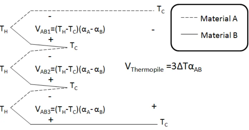
When an electrically conducting material, as the one shown in Figure 2.4, is placed with both ends at different temperatures, a voltage known as the net Seebeck electromotive force (emf) is generated between the ends of the material. The ratio of the net change of Seebeck emf that results from a temperature difference in a single material is called the absolute Seebeck coefficient , and is described by [21]:
14
Figure 2.4 Voltage generated by a temperature difference in a thermoelectric material, where T_H is at a
higher te perature tha T_C a d α_A is the a solute See e k coefficient of the material A
When two dissimilar thermoelectric materials are joined at both ends and one end is heated, there is a continuous current which flows in the circuit. If this circuit is broken, the open circuit voltage is a function of the junction temperature and the Seebeck effect of the two materials [22]. This specific configuration is known as the basic thermocouple and it is shown in Figure 2.5. The output voltage of the thermocouple is obtained through Kirchhoff’s Law:
where is the temperature difference between the hot and cold junctions and is the difference between the absolute Seebeck coefficients of the materials, also known as the relative Seebeck coefficient of the material pair.
Figure 2.5 Basic thermocouple
A thermopile, as the one shown in Figure 2.6, is an array of thermocouples connected thermally in parallel, but electrically in series. Connecting thermocouples in such a way increments the output voltage times. Thus, the output voltage obtained with a thermopile, taking equation (2.5) into account, is described by:
thermopile thermocouple
15
Figure 2.6 Basic structure of a thermopile with z=3
When fabricating thermopiles in a micro scale, usually a thin membrane is connected to a silicon bulk working as a heat sink. Incident IR radiation rises the temperature of the membrane creating a temperature difference between hot (on the membrane) and cold (on the bulk) junctions. This temperature difference, as stated in equation (2.6), generates a voltage proportional to the temperature difference itself, to the number of thermocouples and to the relative Seebeck coefficient of the material pair.
This implies that there are three main ways in which the thermopile could be modified to achieve a larger voltage, and thus a better sensitivity: incrementing the number of thermocouples, creating a larger difference between Seebeck coefficients by choosing different materials and incrementing the temperature difference by creating a high thermal insulation of the hot junctions.
2.2.2.1 Number of thermocouples
16
2.2.2.2 Materials used
The Bi/Te (Bismuth Telluride) junction, largely used in thermopile industry, has a Seebeck coefficient of 572 μV⁄ [23], but it is not compatible with standard IC processes and is more difficult to deal with in a MEMS fabrication process [24]. Values as large as, or larger than the one achieved with this combination of materials have been tried to be obtained with different combinations of materials compatible with standard IC processes.
A widely used combination of materials is the Al/poly-Si (Aluminum, polycrystalline Silicon) junction, materials that have already been used for IR sensing [25]. The main reason for using this specific combination is that almost every CMOS process already uses both materials. However, this junction has a Seebeck coefficient an order of magnitude smaller than that of the Bi/Te junction, with a value of ⁄ for the AMS (austriamicrosystems) process [26].
Another combination that has lately been increasing its popularity is the n-poly-Si/p-poly-Si (n-type polycrystalline Silicon, p-type polycrystalline Silicon) junction and it has already been developed for IR sensing achieving a sensitivity of ⁄ in the 1.5 – 3
wavelength range [24]. Depending on the fabrication process, p-poly-Si can achieve a Seebeck coefficient from to ⁄ and n-poly-Si from to ⁄
[27]. The Seebeck coefficient of this junction depends on the fabrication process because several variables contribute to its value, for n-doped Si its behavior is described by:
[ ( ) ]
where is the Boltzmann constant, is the conduction band density of states, is the electron density, is the exponent describing the relation between relaxation time and charge carrier energy and is the contribution of acoustic phonons dragging charge carriers towards the cold side of the cristal [28].
17
2.2.2.3 Thermal insulation
Another way of achieving a better performance from a thermopile is by creating a high thermal insulation between the hot and cold junctions. The most basic way for a thermopile to generate this insulation is by placing the thermocouples over a suspended cantilever or bridge membrane, minimizing the heat transfer area. But recently, novel techniques for achieving a better thermal insulation have been developed.
[image:30.612.133.494.354.698.2]A structure has been presented that, in order to realize ideal higher thermal insulation, has a self-supporting structure in no need for a membrane [30]. The main idea of this thermopile is to achieve a maximum bending in the legs of the thermocouples and create almost vertical structures, over which an absorbing material film can be deposited. In the proposed structure, the absorbed heat transfers from the hot junction to the cold junction only through the thermopile itself and no other heat transfer will happen because of the lack of a membrane. As a consequence, temperature difference approaches an ideal value. In Figure 2.7, the ideal structure, fabrication process and obtained structure are shown.
18
Another way of incrementing the thermal insulation is by changing the material used for the membrane of the thermopile. Work has been presented showing that the epoxy based photoresist SU-8 could be used as a self-supported membrane in a thermopile IR detector [31, 32], as the one shown in Figure 2.8. The results obtained by Mattsson et al. in matters of sensitivity are not quite impressive, with values lower than ⁄ , but what is really important is the fact that SU-8 has been proved as a valid membrane material for IR thermopiles, which has a thermal conductivity of ⁄ , much lower than the
⁄ of Si3N4 (Silicon Nitride), material generally used as the membrane. The
backside of this technology resides on the fact that SU-8 is not a material used in IC processes, making its fabrication more complex.
Figure 2.8 Schematic image of the IR thermopile detector with a SiO2/SU-8 2002 membrane [32]
2.3 Selecting a sensor
19
Si based thermal detectors can easily work in the IR spectral range and have already been fabricated with a CMOS process followed by a micromachining step [24]. Also, IR thermal detectors can operate at room temperature and have a flat spectral response over a broad wavelength range, characteristics that most IR photonic detectors lack [32]. Among thermal detectors, bolometers and thermopiles stand out for IR sensing, but bolometer-based detectors are susceptible to self-heating effects, are not as simple to fabricate as thermopiles, require electric biasing and show excess current induced noises [13].
Thermopiles have shown a big potential because of their high linearity, the fact that they require no optical chopper and because their detectivity values are comparable to those obtained with other thermal detectors. Also, they operate over a broad temperature range with no need for temperature stabilization, their pink noise is negligible [15], they do not need to be cooled and the fabrication process is relatively simple [33].
21
Chapter III
3
Analytical Model for a CMOS-MEMS Thermopile
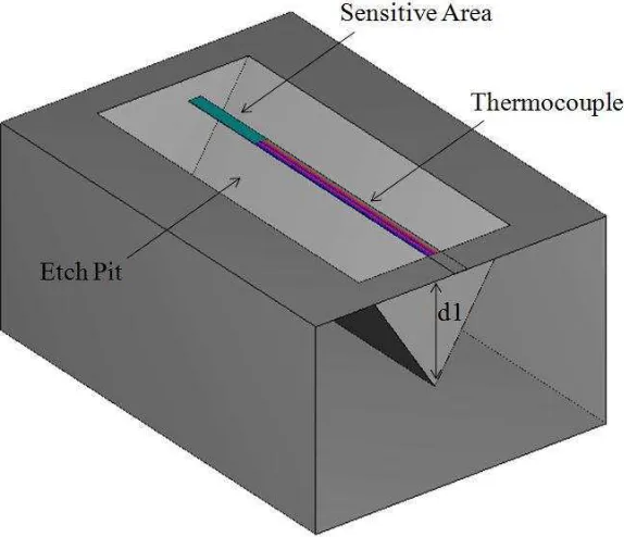
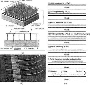
To better understand the behavior of a sensor and to optimize its performance, a mathematical model is needed. A mathematical model for the sensitivity of thermopile infrared detectors on CMOS silicon oxide cantilever beams, isolated by a post-processing anisotropic etching, was obtained by [35] and taken into account for the proposed analytical model developed in this chapter. In this structure, shown in Figure 3.1, while the hot contacts are located at the tip of the membrane, the cold contacts are located at the bulk, working as a heat sink.
Figure 3.1 Thermopile infrared detector on CMOS silicon oxide cantilever beam isolated by post-processing anisotropic etching [35]
22
3.1 Analytical model
To obtain the analytical model, first the geometry related variables were defined as shown in Figure 3.2. In order to calculate the sensitivity, the temperature distribution along the cantilever in the x-direction had to be known. Neglecting the boundary disturbances in the y-direction, the Joule heating effect, assuming a uniform thermal conductivity a uniform temperature across the thin cantilever and assuming all terms remain constant, for
, the temperature distribution along the cantilever in the x-direction was defined as:
t b ( )
[image:35.612.197.447.364.636.2]where the terms represent the heat loss due to conductivity, radiation and convection, respectively. Also, the radiation term only takes into account the radiation heat loss on the upper and lower faces of the membrane. Since the area of the side faces is much smaller than the area of the upper and lower faces, the heat loss on these surfaces is negligible.
Figure 3.2 Top view of cantilever thermopile [35]
23
emissivity of the lower face of the membrane, is the convective heat transfer coefficient of the gas atmosphere, is the thermal conductivity of the cantilever material (also called by some authors) and is the volume of the membrane.
The heat transfer coefficient is defined as [35]:
( )
where is the thermal conductivity of the gas atmosphere, is the distance between the membrane and the bottom of the etch pit, as shown in Figure 3.1 and is the distance between the membrane and the package cap.
Inserting equation (3.2) in equation (3.1) and considering that:
where, as shown in Figure 2.2, is the width of the membrane, is the length of the beam and is the thickness of the membrane, and also factorizing:
( ) ( )
and assuming,
we obtain:
[ t b ]
To find a solution for equation (3.6), it is first rewritten as:
where
√ t b
24
Solving for equation (3.7) yields:
thus, the general solution is described by:
where
and by applying Euler’s identity and trigonometric identities, equation (3.11) turns into:
( )
It can be demonstrated that equation (3.14) is in fact a solution for equation (3.7), considering that
( )
thus,
( )
Now, assuming temperature at equals environmental temperature, and temperature at , as defined by Figure 3.2, equals the temperature at the sensitive area [35], the boundary conditions are defined as:
[ ] ( )
and
[ ] ( )
25 Solving for in equation (3.18) yields:
( )
thus, by inserting equation (3.19) in equation (3.14), the temperature distribution is obtained:
( )
( )
The temperature increase is then calculated using the heat-balance condition [35]:
{ t [ t b ] }
where is the irradiance given in W/m2. To solve such equation for , we first obtain the first derivative of :
|
( )
( ) ( )
and by inserting equation (3.22) in equation (3.21) we obtain:
( ) { t [ t b ] }
The temperature increase equation is found by solving equation (3.23) for and is described by:
[ t b ] ( )
As it was already stated, the sensitivity for a thermal detector is defined as the ratio of the signal voltage to the incident radiation power . The signal voltage is defined in equation (2.6) and the incident radiation power is given by:
thus, the sensitivity of the system is:
26
3.2 Thermocouples as part of the membrane
Optimization of the geometry of the thermopile is critical to achieve a good performance of the device. Because of this, it is of interest to study how the width, length, number and thermal properties of the thermocouples affect the behavior of the sensor. But, equation (3.21) does not take into account some of these parameters. Thus, modifications to the model had to be made in order to insert these variables and to analyze them in terms of the performance of the thermopile.
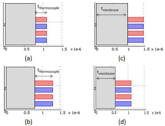
[image:39.612.176.463.353.600.2]Regarding the analytical model, thermopiles can be thought of as part of the membrane, constituting a bi-layer membrane with different characteristics than the one modeled previously. This means that modifying a parameter such as the thickness, in the membrane, would translate into a change of temperature proportional to the one achieved by varying the thickness of the thermocouples. To prove this hypothesis, generic thermopiles, as the one shown in Figure 3.3, were designed using the engineering, design, and finite element analysis environment, COMSOL Multiphysics®.
Figure 3.3 Cantilever thermopile designed using COMSOL Multiphysics®. The anterior face is suppressed for visualization purposes
The basic structure consists of a Si3N4 cantilever membrane on a Si bulk, with two
27
Table 3.1 Values of the geometry parameters used in the COMSOL® design shown in Figure 3.3
Parameter Value [μm]
Wmembrane 36
Wthermocouple 4
Lmembrane 900
Lthermocouple 650
Lsensitive area 250
tmembrane .5 to 1
tthermocouple .5 to 1
d1 350
d2
Twelve thermopiles were designed, six with a fixed membrane thickness of 800 nm, but with a thermocouple thickness varying from 500 to 1000 nm with 100 nm steps. The other six thermocouples had a fixed thermocouple thickness of 500 nm, but with a membrane thickness varying from 500 to 1000 nm with 100 nm steps. This design is illustrated in Figure 3.4, where the variation in the thicknesses of the thermocouples and the membrane are shown. The parameter d2 was assumed as infinite since the package cap was
not designed.
Figure 3.4 Thermocouples designed using COMSOL® with (a) tthermocouple = 0.3 μm, tmembrane = 0.8 μm,
[image:40.612.184.454.449.656.2]28
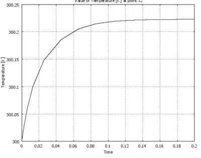
A curve for the temperature at the sensitive area, as the one shown in Figure 3.5, was obtained for each thermopile designed. Using Mathwork’s® high-level technical computing
[image:41.612.121.520.205.519.2]language, MATLAB®, the maximum temperatures detected were normalized and plotted either as a function of the thickness of the thermocouples or the membrane. Two similar curves were expected for the thermocouples to accurately be considered as part of the membrane in the analytical model.
Figure 3.5 Temperature at the sensitive area of the thermopile shown in Figure 3.3 vs. Time, obtained with COMSOL®
29
Figure 3.6 Relationship between the thicknesses of the thermocouples and the membrane
To insert the parameters of the thermocouple in the analytical model, considering it as a component of the membrane, a few changes had to be made. Since the thermocouples have a non-rectangular geometry and are not as long as the beam, equation (3.3) needs an additional term:
where is the width of the membrane (previously called ), is the thickness of the membrane, is the thickness of the thermocouples, is the length of the thermocouples, is the thickness of the thermocouples , is the volume of the membrane as given by equation (3.3), and is the volume contribution of the thermocouples.
Because of this, the simplification:
used in equation (3.6) needs to be modified and considering that the thermal conductivity of the bi-layered cantilever is defined as [35]:
500 550 600 650 700 750 800 850 900 950 1000 0 0.1 0.2 0.3 0.4 0.5 0.6 0.7 0.8 0.9 1
Thickness of Membrane/Thermocouples [m]
N o rm a liz e d T e m p e ra tu re D if fe re n c e
30 then, equation (3.28) has to be changed to:
( ) ( ) ( ) ( )
thus, the new parameter is defined as:
√ t b
and consequently, the sensitivity for the proposed model becomes:
[ t b ] ( )
Equation (3.32) shows that the sensitivity has a dependency on the geometry, the fabrication process, and the materials used. In Chapter IV, a thorough discussion on whether each parameter depends on the fabrication process, the geometry, or the material used is made.
3.3 Validation of the proposed model
The proposed analytical model was tested using MATLAB®. The values of the parameters of the thermopile used for the simulations are shown in Table 3.2 Those same parameters were used for designing a thermopile as the one shown in Figure 3.3 with COMSOL®, so that the results of the analytical model obtained with MATLAB® could be compared with the results of the structure analyzed using COMSOL®.
Table 3.2 Parameters of the thermopile used in both MATLAB® and COMSOL®
Parameter Value Parameter Value
[ ]
[ ]
[ ] [ ] [ ]
[ ] [ ]
[ ] [ ]
31
In the simulation range, varying the thickness of the thermocouples from 500 to 1000 nm, a maximum error between the analytical and the finite element analysis for the temperature difference of 4.69% was obtained. Also, as shown in Figure 3.7, the behavior of both curves seems to be similar, which leads to the assumption that the error obtained between both methods is not due to the thickness of the thermocouples.
Figure 3.7 Temperature difference vs. Thickness of the thermocouples for both the analytical and the finite element analysis
To better prove this hypothesis, the results were normalized in order to find the similarity in the behavior of both curves. The normalization consisted in subtracting the smallest value and dividing over the largest value minus the smallest value for each curve. With the normalized curves, as shown in Figure 3.8, a maximum error between curves of 1.73% was obtained, demonstrating that both curves respond in an almost identical way for a change in the thickness of the thermocouples. These results demonstrate that the proposed analytical model, can accurately determine the changes in the temperature difference that a change in the parameters of the thermocouple generates. Therefore, the output voltage and the sensitivity can also be accurately obtained.
0.5 0.55 0.6 0.65 0.7 0.75 0.8 0.85 0.9 0.95 1
0.17 0.18 0.19 0.2 0.21 0.22 0.23 0.24
Thickness of Thermocouples [m]
32
Figure 3.8 Normalized temperature difference vs. Thickness of thermocouples for both the analytical and the finite element analysis
0.5 0.55 0.6 0.65 0.7 0.75 0.8 0.85 0.9 0.95 1
0 0.1 0.2 0.3 0.4 0.5 0.6 0.7 0.8 0.9 1
Thickness of Thermocouples [m]
33
Chapter IV
4
Design Optimization
The parameters that affect the sensitivity of the thermopile can be found in equation (3.32), and can by classified in 3 different groups: fabrication process dependent parameters, material dependent parameters and geometry dependent parameters. In order to increase the sensitivity of the device by optimizing the design, these variables are analyzed next.
4.1 Fabrication process dependent parameters
Since these parameters depend solely on the chosen fabrication process, there is not really any optimization that can be done to them. The only way to achieve a better sensitivity through the indirect manipulation of these parameters is by selecting the fabrication process with the best characteristics for this specific application. The parameters that depend on the fabrication process are: the distance between the cantilever and the bottom of the etch pit , the distance between the cantilever and the package cap , the thermal conductivity of the gas atmosphere , the thickness of the thermocouples , the thickness of the membrane and the width of the thermocouples .
It is easy to see why the first three parameters depend solely on the fabrication process, but that may not be the case with the rest of the previously mentioned parameters. Thicknesses and widths seem to belong to the geometry dependent parameter class, but that is actually not the case. It was already demonstrated, in Figure 3.6, that the thinner the thermocouples and the membrane, the larger the temperature difference. Also, according to equation (2.6), a large temperature difference translates into a large output voltage, which according to equation (3.26) translates into an increase in the sensitivity. Because of this, the membrane and the thermocouples will be designed as thin as the fabrication process allows them to be and not with a specific designer defined value. Thus, the geometry dependency for both of these parameters disappears, making them fabrication process dependent parameters.
34
[image:47.612.130.495.246.541.2]thermocouples and the membrane, the slimmer the thermocouples, the higher the sensitivity. This characteristic is shown in Figure 4.1, where it can be seen that the highest sensitivity is achieved with the smallest value for the width of the thermocouples. Thus, the critical dimension of the process, referring to the line width particularly, will be used for the width of the thermocouples, eliminating the geometry dependency for this parameter as well. In this figure, by assuming the curve as linear, a slope with a value of -3.57 is obtained. This indicates that for every extra micrometer that the thermocouples are widened, 3.57 V/W are approximately loss in sensitivity.
Figure 4.1 Sensitivity of the thermopile when the width of the thermocouples is varied
The critical dimension of a process is defined as “the absolute size of a minimum feature in an IC or a miniature device, whether it involves a line width, spacing, or contact dimensions” [36]. Figure 4.1 was obtained by programming in MATLAB® the analytical
35
Table 4.1 Parameters for the simulation in which the width of the thermocouples was varied
Parameter Value Parameter Value
[ ]
[ ]
[ ]
[ ] [ ]
[ ] [ ]
[ ] [ ] [ ] [ ]
[ ]
4.2 Material dependent parameters
The parameters that depend on the selection of the materials are: the Seebeck coefficient , the emissivity of the sensitive area on the lower face , and the emissivity of the sensitive area on the upper face . The Seebeck effect has been discussed in Chapter II, making the dependency of the Seebeck coefficient on the material chosen obvious. However, this parameter could also be classified as fabrication process dependent. As it has already been mentioned, an intention in making the thermopile IC compatible exists, and in order to achieve this, the material selection for the thermocouples must be restricted to the materials available in the IC fabrication process. This restriction of materials makes the Seebeck coefficient not only material dependent, but also fabrication process dependent.
36
4.3 Geometry dependent parameters
The parameters of the thermopile that can most easily be manipulated in order to optimize the design, increasing the sensitivity, are the geometry dependent parameters. The geometry dependent parameters of the thermopile are: the width of the membrane , the length of the sensitive area , the length of the thermocouples , the length of the membrane and the number of thermocouples .
4.3.1 Width of the membrane
[image:49.612.128.497.378.672.2]Increasing the width of the membrane does not improve the performance of the thermopile, but it can indirectly do so. In fact, as is it shown in Figure 4.2, as the membrane widens, the sensitivity decreases. It is important to clarify that in the simulation carried out to obtain this curve, the number of thermocouples remains fixed. The rest of the parameters were set to the values shown in Table 4.1, with the exception of the width of the thermocouples, set to 4 μm and the width of the membrane, varied from 26 to 300 m.
37
However, widening the membrane can help in enhancing the performance of the thermopile, because as the membrane widens, the maximum number of thermocouples that can fit increases. And as it will be discussed later in this chapter, increasing the number of thermocouples translates into a larger sensitivity.
4.3.2 Length of the thermocouples and length of the sensitive area
The maximum length of the thermocouples and of the sensitive area is restrained by the length of the membrane and by each other. Regarding fabrication, the sum of both of these lengths must be equal or smaller than the length of the entire membrane. Because of this, an analysis has been made to optimize the design of the thermopile by finding the best length of the thermocouples to length of the sensitive area ratio in terms of sensitivity.
Using the proposed analytical model obtained in Chapter III, a simulation was made using MATLAB®. In this simulation, the parameters were set to the values shown in Table 4.2, varying the length of the sensitive area from 4 to 996 m and defining the length of the thermocouples as the length of the membrane minus the length of the sensitive area.
Table 4.2 Parameters for the simulation in which the length of the thermocouples and the length of the sensitive area were varied
Parameter Value Parameter Value
[ ] [ ] [ ]
[ ] [ ]
[ ] [ ]
.0262 [ ]
[ ] [ ] [ ]
38
Figure 4.3 Sensitivity of the thermopile when the length of the sensitive area and the length of the thermocouples are varied
39
Figure 4.4 Thermopiles designed using COMSOL® with (a) thermocouples length of 650 μm and sensitive area length of 250 μm; (b) thermocouples length of 250 μm and sensitive area length of 650 μm
The curves shown in Figure 4.5 represent the signal obtained for each thermopile. After acquiring that data, the response time for each signal was determined. The response time is defined as the time it takes for a signal to achieve 0.6321 times the maximum value of the signal. It can be seen in Figure 4.6 that the maximum response time occurs when the length of the thermocouple equals the length of the sensitive area. The smallest values for the response time appear when the thermocouples are either the shortest or the longest within the simulation. Thus, lengthening the thermocouples not only increases the sensitivity, but also reduces the response time. However, it can be seen that the actual time that can be reduced or increased by manipulating these parameters does not exceed a couple of milliseconds.
40
Figure 4.6 Response time vs. length of the thermocouples
4.3.3 Length of the membrane
41
Figure 4.7 Sensitivity of the thermopile when the length of the membrane is varied
[image:54.612.128.500.104.398.2]The results obtained in the previous figure correspond to a simulation with the parameters shown in Table 4.3, where the length of the membrane was varied from 100 to 5000 μm and where the length of the thermocouples was defined as the length of the membrane minus the length of the sensitive area, fixed to 4 μm.
Table 4.3 Parameters for the simulation in which the length of the membrane was varied
Parameter Value Parameter Value
[ ] [ ] [ ]
[ ] [ ]
[ ] [ ]
[ ] [ ] [ ] [ ]
42
4.3.4 Number of thermocouples
The situation with the number of thermocouples is complex, as this parameter is not only geometry dependent, but it also depends at some point on the fabrication process. A simulation similar to the one mentioned for the width of the thermocouples previously in this chapter, was carried out. This simulation was done by varying the number of thermocouples from 2 to 30, and considering a membrane width of 362 μm, in order for up to 30 thermocouples, with a spacing of 2 μm, to fit in the membrane. The values of the rest of the parameters used in this simulation are shown in Table 4.4.
Table 4.4 Parameters for the simulation in which the number of thermocouples was varied
Parameter Value Parameter Value
[ ] [ ] [ ] [ ] [ ]
[ ] [ ]
[ ] [ ] [ ] [ ]
[ ]
43
Figure 4.8 Sensitivity of the thermopile when the number of thermocouples is varied
The maximum number of thermocouples that can fit in a cantilever membrane with a specific width , depends solely on the minimum spacing and the minimum line width , critical dimensions of the fabrication process, and can be represented by equation (4.1). As it can be seen, the width of the membrane is the only geometry dependent term in such equation. Thus, for a membrane with a specific width, a parameter that is geometry dependent, the maximum number of thermocouples may seem to depend on the fabrication process exclusively.
⌊ ⌋
44
[image:57.612.199.445.128.334.2]that there will be some unused space in the membrane if the width of the membrane is not designed for a specific number of thermocouples according to equation (4.1).
Figure 4.9 Top-view of the membrane of a cantilever thermopile showing the line width and spacing
The maximum number of thermocouples achievable seems to be a fabrication process dependent parameter, but there is a geometry dependency. In order to increment the maximum number of thermocouples, exceeding the value obtained with equation (4.1), there are two viable options, either to widen the membrane or to use a bridge structure instead of the cantilever structure used up to this point. Unfortunately, both options have drawbacks. Since the idea of this project is to fabricate a microspectrophotometer, and the wider the membrane, the bigger the device, it is not ideal to just widen the membrane to obtain a better sensitivity by increasing the maximum number of thermocouples. Also, widening the membrane translates into a larger thermal conduction area, ergo, the sensitivity increases at a slow rate when this parameter is modified.
45
4.3.4.1 Analysis of a thermopile based on a bridge structure
[image:58.612.113.535.276.485.2]The reason why a thermopile with a bridge structure can approximately double the number of thermocouples from a thermopile with a cantilever structure resides on the possibility to place thermocouples in both sides of the bridge, in contact with the bulk. As it is shown in Figure 4.10, a bridge structure needs a thermocouple to cross the bridge in order for the thermal series connection to maintain. It is because of this particular thermocouple, that the maximum number of thermocouples between a bridge and a cantilever structure does not exactly double. Depending on the width of the membrane and the critical dimensions mentioned previously, there will either be or thermocouples, where is the number of thermocouples in the cantilever structure.
Figure 4.10 Top-view of a thermopile (a) based on a cantilever structure and (b) based on a bridge structure
A bridge structure can be analyzed as a cantilever structure with a sensitive area half as long and thermocouples, using the proposed analytical model. This asseveration was proven right in the same way as the analytical model was proved right in Chapter III. Six n-poly-Si/p-poly-Si thermopiles based on a Si3N4 bridge structure, as the one shown in
46
Table 4.5 Values of the geometry parameters used in the COMSOL® design of the bridge based thermopiles
Parameter Value [μm]
Wm 36
Wt 4
Lm 982
Lt 341
Ls 300
tm .8
tt .3 to .8
d1 400
[image:59.612.106.537.332.561.2]d2
Figure 4.11 Thermopile based on a bridge structure designed using COMSOL Multiphysics®. In the zoomed image, the thermocouple junction at the sensitive area is shown
47
done because, as it was already stated, to fit a bridge structure in the analytical model, it must be considered as a cantilever structure with half the length of the bridge structure.
Table 4.6 Parameters for the simulation in which the thickness of the thermocouples was varied for a bridge structure
Parameter Value Parameter Value
[ ]
[ ]
[ ]
[ ] [ ]
[ ] [ ]
[ ] [ ] [ ] [ ]
[ ]
For the analytical model to accurately represent the behavior of the thermopile based on a bridge structure, a small detail had to be changed in equation (3.27). In this equation, the volume contribution of the thermocouples to the membrane is defined as
but for a bridge structure, the volume contribution of the thermocouples must be represented by
since the number of thermoelements (a single leg of the thermocouple) in one side of the bridge is exactly , while in the case of the cantilever structure, the number of thermoelements in the membrane is .
![Figure 1.1 Predicted vs. measured blood glucose levels [3]](https://thumb-us.123doks.com/thumbv2/123dok_es/4458674.35719/14.612.216.426.371.578/figure-predicted-vs-measured-blood-glucose-levels.webp)
![Figure 2.2 Generic structure of the InP/InGaAs photodetector [17]](https://thumb-us.123doks.com/thumbv2/123dok_es/4458674.35719/24.612.110.534.406.644/figure-generic-structure-inp-ingaas-photodetector.webp)
![Figure 2.3 Simplified process of a Vanadium Oxide microbolometer [15]](https://thumb-us.123doks.com/thumbv2/123dok_es/4458674.35719/26.612.107.529.88.342/figure-simplified-process-of-a-vanadium-oxide-microbolometer.webp)
![Figure 3.2 Top view of cantilever thermopile [35]](https://thumb-us.123doks.com/thumbv2/123dok_es/4458674.35719/35.612.197.447.364.636/figure-view-cantilever-thermopile.webp)