2
1 7
10
9 15
3
6
11
14 1A
1,2EN
2A
3A
3,4EN
4A
1Y
2Y
3Y
4Y
L293, L293D
SLRS008D – SEPTEMBER 1986 – REVISED JANUARY 2016
L293x Quadruple Half-H Drivers
1 Features
3 Description
The L293 and L293D devices are quadruple
high-1• Wide Supply-Voltage Range: 4.5 V to 36 V
current half-H drivers. The L293 is designed to • Separate Input-Logic Supply
provide bidirectional drive currents of up to 1 A at • Internal ESD Protection voltages from 4.5 V to 36 V. The L293D is designed to provide bidirectional drive currents of up to 600-mA • High-Noise-Immunity Inputs
at voltages from 4.5 V to 36 V. Both devices are • Output Current 1 A Per Channel (600 mA for
designed to drive inductive loads such as relays, L293D)
solenoids, DC and bipolar stepping motors, as well as • Peak Output Current 2 A Per Channel (1.2 A for other high-current/high-voltage loads in
positive-L293D) supply applications.
• Output Clamp Diodes for Inductive Transient Each output is a complete totem-pole drive circuit, Suppression (L293D) with a Darlington transistor sink and a pseudo-Darlington source. Drivers are enabled in pairs, with
2 Applications
drivers 1 and 2 enabled by 1,2EN and drivers 3 and 4enabled by 3,4EN. • Stepper Motor Drivers
The L293 and L293D are characterized for operation • DC Motor Drivers
from 0°C to 70°C. • Latching Relay Drivers
Device Information(1)
PART NUMBER PACKAGE BODY SIZE (NOM)
L293NE PDIP (16) 19.80 mm × 6.35 mm
L293DNE PDIP (16) 19.80 mm × 6.35 mm
(1) For all available packages, see the orderable addendum at the end of the data sheet.
Logic Diagram
Table of Contents
8.3 Feature Description...7
1 Features...1
8.4 Device Functional Modes...8
2 Applications...1
9 Application and Implementation...9
3 Description...1
9.1 Application Information...9
4 Revision History...2
9.2 Typical Application ...9
5 Pin Configuration and Functions...3
9.3 System Examples ...10
6 Specifications...4
10 Power Supply Recommendations...13
6.1 Absolute Maximum Ratings ...4
11 Layout...14
6.2 ESD Ratings...4
11.1 Layout Guidelines ...14
6.3 Recommended Operating Conditions ...4
11.2 Layout Example ...14
6.4 Thermal Information ...4
12 Device and Documentation Support...15
6.5 Electrical Characteristics...5
12.1 Related Links ...15
6.6 Switching Characteristics ...5
12.2 Community Resources...15
6.7 Typical Characteristics ...5
12.3 Trademarks ...15
7 Parameter Measurement Information...6
12.4 Electrostatic Discharge Caution ...15
8 Detailed Description...7
12.5 Glossary ...15
8.1 Overview ...7
13 Mechanical, Packaging, and Orderable 8.2 Functional Block Diagram ...7
Information...15
4 Revision History
NOTE: Page numbers for previous revisions may differ from page numbers in the current version. Changes from Revision C (November 2004) to Revision D Page • RemovedOrdering Informationtable ... 1HEAT SINK AND GROUND HEAT SINK AND
GROUND 1
2
3
4
5
6
7
8 16
15
14
13
12
11
10
9 1,2EN
1A 1Y
2Y 2A VCC2
VCC1
4A 4Y
3Y 3A 3,4EN
5 Pin Configuration and Functions
NE Package 16-Pin PDIP Top View
Pin Functions PIN
TYPE DESCRIPTION
NAME NO.
1,2EN 1 I Enable driver channels 1 and 2 (active high input)
<1:4>A 2, 7, 10, 15 I Driver inputs, noninverting
<1:4>Y 3, 6, 11, 14 O Driver outputs
3,4EN 9 I Enable driver channels 3 and 4 (active high input)
Device ground and heat sink pin. Connect to printed-circuit-board ground plane with multiple GROUND 4, 5, 12, 13 — solid vias
6 Specifications
6.1 Absolute Maximum Ratings
over operating free-air temperature range (unless otherwise noted)(1)
MIN MAX UNIT
Supply voltage, VCC1(2) 36 V
Output supply voltage, VCC2 36 V
Input voltage, VI 7 V
Output voltage, VO –3 VCC2+ 3 V
Peak output current, IO(nonrepetitive, t≤5 ms): L293 –2 2 A
Peak output current, IO(nonrepetitive, t≤100 µs): L293D –1.2 1.2 A
Continuous output current, IO: L293 –1 1 A
Continuous output current, IO: L293D –600 600 mA
Maximum junction temperature, TJ 150 °C
Storage temperature, Tstg –65 150 °C
(1) Stresses beyond those listed underAbsolute Maximum Ratingsmay cause permanent damage to the device. These are stress ratings only, which do not imply functional operation of the device at these or any other conditions beyond those indicated underRecommended Operating Conditions. Exposure to absolute-maximum-rated conditions for extended periods may affect device reliability.
(2) All voltage values are with respect to the network ground terminal.
6.2 ESD Ratings
VALUE UNIT
Human-body model (HBM), per ANSI/ESDA/JEDEC JS-001(1) ±2000 Electrostatic
V(ESD) discharge V
Charged-device model (CDM), per JEDEC specification JESD22-C101(2) ±1000 (1) JEDEC document JEP155 states that 500-V HBM allows safe manufacturing with a standard ESD control process. (2) JEDEC document JEP157 states that 250-V CDM allows safe manufacturing with a standard ESD control process.
6.3 Recommended Operating Conditions
over operating free-air temperature range (unless otherwise noted)
MIN NOM MAX UNIT
VCC1 4.5 7
Supply voltage V
VCC2 VCC1 36
VCC1≤7 V 2.3 VCC1 V
VIH High-level input voltage
VCC1≥7 V 2.3 7 V
VIL Low-level output voltage –0.3(1) 1.5 V
TA Operating free-air temperature 0 70 °C
(1) The algebraic convention, in which the least positive (most negative) designated minimum, is used in this data sheet for logic voltage levels.
6.4 Thermal Information
L293, L293D
THERMAL METRIC(1) NE (PDIP) UNIT
16 PINS
RθJA Junction-to-ambient thermal resistance(2) 36.4 °C/W
RθJC(top) Junction-to-case (top) thermal resistance 22.5 °C/W
RθJB Junction-to-board thermal resistance 16.5 °C/W
ψJT Junction-to-top characterization parameter 7.1 °C/W
ψJB Junction-to-board characterization parameter 16.3 °C/W
(1) For more information about traditional and new thermal metrics, see theSemiconductor and IC Package Thermal Metricsapplication report,SPRA953.
5
3
1
0 2
−50 0 50
4
100
TA− Ambient Temperature −°C With Infinite Heat Sink
Free Air Heat Sink WithθJA= 25°C/W
150 PT O T − P o w e r D is s ip a ti o n − W
6.5 Electrical Characteristics
over operating free-air temperature range (unless otherwise noted)
PARAMETER TEST CONDITIONS MIN TYP MAX UNIT
L293: IOH=−1 A
VOH High-level output voltage VCC2– 1.8 VCC2– 1.4 V
L293D: IOH=−0.6 A
L293: IOL= 1 A
VOL Low-level output voltage 1.2 1.8 V
L293D: IOL= 0.6 A
VOKH High-level output clamp voltage L293D: IOK= –0.6 A VCC2+ 1.3 V
VOKL Low-level output clamp voltage L293D: IOK= 0.6 A 1.3 V
A 0.2 100
IIH High-level input current VI= 7 V µA
EN 0.2 10
A –3 –10
IIL Low-level input current VI= 0 µA
EN –2 –100
All outputs at high level 13 22 All outputs at low level 35 60
ICC1 Logic supply current IO= 0 mA
All outputs at high
8 24
impedance
All outputs at high level 14 24 All outputs at low level 2 6
ICC2 Output supply current IO= 0 mA
All outputs at high
2 4
impedance
6.6 Switching Characteristics
over operating free-air temperature range (unless otherwise noted) VCC1= 5 V, VCC2= 24 V, TA= 25°C
PARAMETER TEST CONDITIONS MIN TYP MAX UNIT
L293NE, L293DNE 800
Propagation delay time,
low-to-tPLH high-level output from A input ns
L293DWP, L293N L293DN 750
L293NE, L293DNE 400
Propagation delay time,
high-to-tPHL low-level output from A input ns
L293DWP, L293N L293DN C 200
L= 30 pF,
SeeFigure 2
L293NE, L293DNE 300
Transition time, low-to-high-level
tTLH output ns
L293DWP, L293N L293DN 100
L293NE, L293DNE 300
Transition time, high-to-low-level
tTHL output ns
L293DWP, L293N L293DN 350
6.7 Typical Characteristics
Output
CL= 30 pF
(see Note A) VCC1
Input
3 V
TEST CIRCUIT
tf tr
3 V
0
tPHL
VOH
tTHL tTLH
VOLTAGE WAVEFORMS tPLH
Output Input
VOL
tw
NOTES: A. CLincludes probe and jig capacitance.
B. The pulse generator has the following characteristics: tr≤10 ns, tf≤10 ns, tw= 10 µs, PRR = 5 kHz, ZO= 50 Ω.
Pulse Generator (see Note B)
5 V 24 V
VCC2
A
EN
Y
90% 90%
50%
10% 50%
10%
90% 90%
50%
10%
50%
10%
7 Parameter Measurement Information
1 0
3 4 5 6
7
8 9
10 11 12 13 14 15 16 1
2 1 0
1
1 0
2
4
3
M M
M
1 0
1 0 1 0
VCC2
VCC1
8 Detailed Description
8.1 Overview
The L293 and L293D are quadruple high-current half-H drivers. These devices are designed to drive a wide array of inductive loads such as relays, solenoids, DC and bipolar stepping motors, as well as other high-current and high-voltage loads. All inputs are TTL compatible and tolerant up to 7 V.
Each output is a complete totem-pole drive circuit, with a Darlington transistor sink and a pseudo-Darlington source. Drivers are enabled in pairs, with drivers 1 and 2 enabled by 1,2EN and drivers 3 and 4 enabled by 3,4EN. When an enable input is high, the associated drivers are enabled, and their outputs are active and in phase with their inputs. When the enable input is low, those drivers are disabled, and their outputs are off and in the high-impedance state. With the proper data inputs, each pair of drivers forms a full-H (or bridge) reversible drive suitable for solenoid or motor applications.
On the L293, external high-speed output clamp diodes should be used for inductive transient suppression. On the L293D, these diodes are integrated to reduce system complexity and overall system size. A VCC1 terminal, separate from VCC2, is provided for the logic inputs to minimize device power dissipation. The L293 and L293D are characterized for operation from 0°C to 70°C.
8.2 Functional Block Diagram
Output diodes are internal in L293D.
8.3 Feature Description
VCC2
Output
GND VCC2
Output
GND
Input VCC1
Current Source
GND
8.4 Device Functional Modes
Table 1lists the fuctional modes of the L293x.
Table 1. Function Table (Each Driver)(1)
INPUTS(2)
OUTPUT (Y)
A EN
H H H
L H L
X L Z
(1) H = high level, L = low level, X = irrelevant, Z = high impedance (off) (2) In the thermal shutdown mode, the output is in the high-impedance
state, regardless of the input levels.
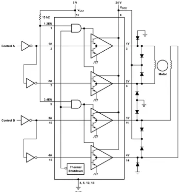
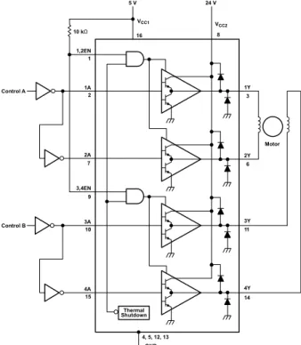
Figure 3. Schematic of Inputs for the L293x
24 V 5 V
10 kΩ
VCC1
VCC2
Control A
Control B
4, 5, 12, 13
GND Thermal Shutdown
Motor
16 8
3
6
11
14 4Y 3Y 2Y 1Y 1,2EN
1A
2A
3,4EN
3A
4A 15 10 9 7 2 1
9 Application and Implementation
NOTE
Information in the following applications sections is not part of the TI component specification, and TI does not warrant its accuracy or completeness. TI’s customers are responsible for determining suitability of components for their purposes. Customers should validate and test their design implementation to confirm system functionality.
9.1 Application Information
A typical application for the L293 device is driving a two-phase motor. Below is an example schematic displaying how to properly connect a two-phase motor to the L293 device.
Provide a 5-V supply to VCC1and valid logic input levels to data and enable inputs. VCC2must be connected to a power supply capable of supplying the needed current and voltage demand for the loads connected to the outputs.
9.2 Typical Application
Figure 6. Two-Phase Motor Driver (L293)
9.2.1 Design Requirements
The design techniques in the application above as well as the applications below should fall within the following design requirements.
1. VCC1should fall within the limits described in theRecommended Operating Conditions. 2. VCC2should fall within the limits described in theRecommended Operating Conditions. 3. The current per channel should not exceed 1 A for the L293 (600mA for the L293D).
9.2.2 Detailed Design Procedure
24 V 5 V
10 kΩ
VCC1 VCC2
16 8 1,2EN 1 1A 2 2A 7 3,4EN 9 3A 10 4A 15 Control A Control B
4, 5, 12, 13 GND Thermal Shutdown Motor 1Y 3 2Y 6 3Y 11 4Y 14 3 1 0 2
0 10 20
P 4 30 T O T − P o w e r D is s ip a ti o n − W 60 20 0 40 80 θJA − T h e rm a l R e s is ta n c e − ° C/W 40
Side − mm
θJA
PTOT(TA= 70°C)
50
Typical Application (continued)
9.2.3 Application Curve
Refer to Power Supply Recommendations for additional information with regards to appropriate power dissipation.Figure 7describes thermal dissipation based onFigure 14.
Figure 7. Maximum Power and Junction vs Thermal Resistance
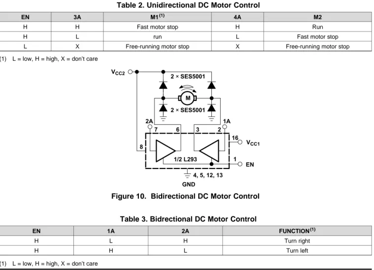
9.3 System Examples
9.3.1 L293D as a Two-Phase Motor Driver
Figure 8 below depicts a typical setup for using the L293D as a two-phase motor driver. Refer to the
Recommended Operating Conditionswhen considering the appropriate input high and input low voltage levels to enable each channel of the device.
2×SES5001
1/2 L293
4, 5, 12, 13 3 6 7
8
1 2
16 VCC2
2×SES5001
2A 1A
VCC1
EN M
GND VCC2
SES5001
1/2 L293
4, 5, 12, 13 10
SES5001
VCC1
EN 15
11 14
16
9 M2 M1
3A 4A
8
GND System Examples (continued)
9.3.2 DC Motor Controls
Figure 9andFigure 10below depict a typical setup for using the L293 device as a controller for DC motors. Note
that the L293 device can be used as a simple driver for a motor to turn on and off in one direction, and can also be used to drive a motor in both directions. Refer to the function tables below to understand unidirectional vs bidirectional motor control. Refer to the Recommended Operating Conditionswhen considering the appropriate input high and input low voltage levels to enable each channel of the device.
Connections to ground and to supply voltage
Figure 9. DC Motor Controls
Table 2. Unidirectional DC Motor Control
EN 3A M1(1) 4A M2
H H Fast motor stop H Run
H L run L Fast motor stop
L X Free-running motor stop X Free-running motor stop
(1) L = low, H = high, X = don’t care
Figure 10. Bidirectional DC Motor Control
Table 3. Bidrectional DC Motor Control
EN 1A 2A FUNCTION(1)
H L H Turn right
H H L Turn left
3
4
5
6
7
8 1
2
9 10 11 12 13 14 15 16
+
+
+
+
D7
D8 D4
D3
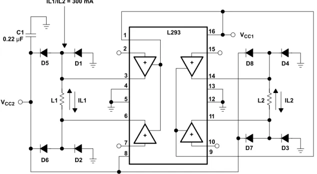
L2 IL2
C1
D5 D1
D6 D2
VCC1
L293 IL1/IL2 = 300 mA
0.22µF
VCC2 L1 IL1
D1−D8 = SES5001
Table 3. Bidrectional DC Motor Control (continued)
EN 1A 2A FUNCTION(1)
H L L Fast motor stop
H H H Fast motor stop
L X X Free-running motor stop
9.3.3 Bipolar Stepping-Motor Control
Figure 11 below depicts a typical setup for using the L293D as a two-phase motor driver. Refer to the
Recommended Operating Conditionswhen considering the appropriate input high and input low voltage levels to enable each channel of the device.
11.9 mm
17.0 mm
38.0 mm
10 Power Supply Recommendations
VCC1is 5 V ± 0.5 V and VCC2can be same supply as VCC1or a higher voltage supply with peak voltage up to 36 V. Bypass capacitors of 0.1 uF or greater should be used at VCC1 and VCC2 pins. There are no power up or power down supply sequence order requirements.
Properly heatsinking the L293 when driving high-current is critical to design. The Rthj-amp of the L293 can be reduced by soldering the GND pins to a suitable copper area of the printed circuit board or to an external heat sink.
Figure 14shows the maximum package power PTOT and the θJA as a function of the side of two equal square
copper areas having a thickness of 35μm (see Figure 14). In addition, an external heat sink can be used (see
Figure 12).
During soldering, the pin temperature must not exceed 260°C, and the soldering time must not exceed 12 seconds.
The external heatsink or printed circuit copper area must be connected to electrical ground.
Copper Area 35-µm Thickness
Printed Circuit Board
5V
TTL Logic
1 Ampere TTL Logic
1 Ampere
GND VIAS TTL Logic
5V to 36V 1 Ampere
TTL Logic
1 Ampere
TTL Logic
TTL Logic 14
13 15 1
2
3
4
16 GND
0.1μF 1,2EN
1A
1Y
VCC1
4A
4Y
10
9 11 12
7
8 6 5
2Y
2A
VCC2
3Y
3A
3,4EN
GND 1μF
11 Layout
11.1 Layout Guidelines
Place the device near the load to keep output traces short to reduce EMI. Use solid vias to transfer heat from ground pins to ground plane of the printed-circuit-board.
11.2 Layout Example
Figure 13. Layout Diagram
12 Device and Documentation Support
12.1 Related Links
The table below lists quick access links. Categories include technical documents, support and community resources, tools and software, and quick access to sample or buy.
Table 4. Related Links
TECHNICAL TOOLS & SUPPORT & PARTS PRODUCT FOLDER SAMPLE & BUY
DOCUMENTS SOFTWARE COMMUNITY
L293 Click here Click here Click here Click here Click here
L293D Click here Click here Click here Click here Click here
12.2 Community Resources
The following links connect to TI community resources. Linked contents are provided "AS IS" by the respective contributors. They do not constitute TI specifications and do not necessarily reflect TI's views; see TI'sTerms of Use.
TI E2E™ Online Community TI's Engineer-to-Engineer (E2E) Community.Created to foster collaboration among engineers. At e2e.ti.com, you can ask questions, share knowledge, explore ideas and help solve problems with fellow engineers.
Design Support TI's Design SupportQuickly find helpful E2E forums along with design support tools and contact information for technical support.
12.3 Trademarks
E2E is a trademark of Texas Instruments.
All other trademarks are the property of their respective owners.
12.4 Electrostatic Discharge Caution
These devices have limited built-in ESD protection. The leads should be shorted together or the device placed in conductive foam during storage or handling to prevent electrostatic damage to the MOS gates.
12.5 Glossary
SLYZ022—TI Glossary.
This glossary lists and explains terms, acronyms, and definitions.
13 Mechanical, Packaging, and Orderable Information
www.ti.com 17-Mar-2017
PACKAGING INFORMATION
Orderable Device Status
(1)
Package Type Package Drawing
Pins Package Qty
Eco Plan
(2)
Lead/Ball Finish
(6)
MSL Peak Temp
(3)
Op Temp (°C) Device Marking
(4/5)
Samples
L293DNE ACTIVE PDIP NE 16 25 Pb-Free
(RoHS)
CU NIPDAU N / A for Pkg Type 0 to 70 L293DNE
L293DNEE4 ACTIVE PDIP NE 16 25 Pb-Free
(RoHS)
CU NIPDAU N / A for Pkg Type 0 to 70 L293DNE
L293NE ACTIVE PDIP NE 16 25 Pb-Free
(RoHS)
CU NIPDAU N / A for Pkg Type 0 to 70 L293NE
L293NEE4 ACTIVE PDIP NE 16 25 Pb-Free
(RoHS)
CU NIPDAU N / A for Pkg Type 0 to 70 L293NE
(1)
The marketing status values are defined as follows: ACTIVE: Product device recommended for new designs.
LIFEBUY: TI has announced that the device will be discontinued, and a lifetime-buy period is in effect.
NRND: Not recommended for new designs. Device is in production to support existing customers, but TI does not recommend using this part in a new design. PREVIEW: Device has been announced but is not in production. Samples may or may not be available.
OBSOLETE: TI has discontinued the production of the device.
(2)
Eco Plan - The planned eco-friendly classification: Pb-Free (RoHS), Pb-Free (RoHS Exempt), or Green (RoHS & no Sb/Br) - please check http://www.ti.com/productcontent for the latest availability information and additional product content details.
TBD: The Pb-Free/Green conversion plan has not been defined.
Pb-Free (RoHS): TI's terms "Lead-Free" or "Pb-Free" mean semiconductor products that are compatible with the current RoHS requirements for all 6 substances, including the requirement that lead not exceed 0.1% by weight in homogeneous materials. Where designed to be soldered at high temperatures, TI Pb-Free products are suitable for use in specified lead-free processes. Pb-Free (RoHS Exempt): This component has a RoHS exemption for either 1) lead-based flip-chip solder bumps used between the die and package, or 2) lead-based die adhesive used between the die and leadframe. The component is otherwise considered Pb-Free (RoHS compatible) as defined above.
Green (RoHS & no Sb/Br): TI defines "Green" to mean Pb-Free (RoHS compatible), and free of Bromine (Br) and Antimony (Sb) based flame retardants (Br or Sb do not exceed 0.1% by weight in homogeneous material)
(3)
MSL, Peak Temp. - The Moisture Sensitivity Level rating according to the JEDEC industry standard classifications, and peak solder temperature.
(4)
There may be additional marking, which relates to the logo, the lot trace code information, or the environmental category on the device.
(5)
Multiple Device Markings will be inside parentheses. Only one Device Marking contained in parentheses and separated by a "~" will appear on a device. If a line is indented then it is a continuation of the previous line and the two combined represent the entire Device Marking for that device.
(6)
www.ti.com 17-Mar-2017
Important Information and Disclaimer:The information provided on this page represents TI's knowledge and belief as of the date that it is provided. TI bases its knowledge and belief on information provided by third parties, and makes no representation or warranty as to the accuracy of such information. Efforts are underway to better integrate information from third parties. TI has taken and continues to take reasonable steps to provide representative and accurate information but may not have conducted destructive testing or chemical analysis on incoming materials and chemicals. TI and TI suppliers consider certain information to be proprietary, and thus CAS numbers and other limited information may not be available for release.