A FPGA Implementation of a MIPS RISC Processor
for Computer Architecture Education
By:
Victor P. Rubio, B.S.
vrubio@gauss.nmsu.edu
Advisor:
Dr. Jeanine Cook
jecook@gauss.nmsu.edu
New Mexico State University
Las Cruces New Mexico
ABSTRACT
A FPGA Implementation of a MIPS RISC Processor
for Computer Architecture Education
By
Victor P. Rubio, B.S.
Master of Science
New Mexico State University
Las Cruces, New Mexico
Chair of Committee:
Dr. Jeanine Cook
Electrical Engineering
Date: July 8, 2004
Room: T & B 104
Time: 1:30 PM
Computer organization and design is a common engineering course where students learn
concepts of modern computer architecture. Students often learn computer design by
implementing individual sections of a computer microprocessor using a simulation-only
approach that limits a students experience to software design. This project targets the computer
architecture courses and presents an FPGA (Field Programmable Gate Array) implementation of
a MIPS (Microprocessor without Interlocked Pipeline Stages) RISC (Reduced Instruction Set
Computer) Processor via VHDL (Very high speed integrated circuit Hardware Description
Language) design. The goal of this project is to enhance the simulator based approach by
integrating some hardware design to help the computer architecture students gain a hands-on
experience in hardware-software integration and achieve a better understanding of both the MIPS
single-cycle and pipelined processors as described in the widely used book,
Computer
C
ONTENTS
Page
L
IST OF
T
ABLES
... 4
L
IST OF
F
IGURES
... 5
1 I
NTRODUCTION AND
B
ACKGROUND
... 6
1.1 FPGA
S
... 6
1.2 T
HE
MIPS P
ROCESSOR
... 11
1.3 CAD S
OFTWARE
... 12
2 R
ELATED
W
ORK
... 14
3 FPGA I
MPLEMENTATION OF THE
P
ROCESSOR
... 15
3.1 T
HE
MIPS I
NSTRUCTION
S
ET
A
RCHITECTURE
... 16
3.2 MIPS S
INGLE
-
CYCLE
P
ROCESSOR
... 18
3.3 MIPS S
INGLE
-
CYCLE
P
ROCESSOR
VHDL I
MPLEMENTATION
... 20
3.3.1 I
NSTRUCTION
F
ETCH
U
NIT
... 24
3.3.2 I
NSTRUCTION
D
ECODE
U
NIT
... 25
3.3.3 T
HE
C
ONTROL
U
NIT
... 26
3.3.4 E
XECUTION
U
NIT
... 27
3.3.5 D
ATA
M
EMORY
U
NIT
... 28
3.4 MIPS P
IPELINED
P
ROCESSOR
VHDL I
MPLEMENTATION
... 29
3.4.1 P
IPELINE
H
AZARDS
... 31
3.5 H
ARDWARE
I
MPLEMENTATION
... 36
4 R
ESULTS AND
D
ISCUSSION
... 38
5 C
LASSROOM
I
NTEGRATION
... 42
6 F
UTURE
W
ORK
... 44
7 C
ONCLUSION
... 45
R
EFERENCES
... 46
A
PPENDIX
... 47
A. R
ESOURCES
... 48
B. A
CRONYM
D
EFINITIONS
... 49
C. MIPS S
INGLE
-
CYCLE
– VHDL C
ODE
... 50
D. MIPS S
INGLE
-
CYCLE
– S
IMULATION
... 63
E. MIPS S
INGLE
-
CYCLE
– S
IMULATION
–
SPIM V
ALIDATION
... 64
F. MIPS P
IPELINED
– VHDL C
ODE
... 65
G. MIPS P
IPELINED
– P
IPELINING
S
IMULATION
... 85
H. MIPS P
IPELINED
– P
IPELINING
S
IMULATION
– SPIM V
ALIDATION
... 86
I. MIPS P
IPELINED
– D
ATA
H
AZARD AND
F
ORWARDING
S
IMULATION
... 87
J. MIPS P
IPELINED
– D
ATA
H
AZARD AND
F
ORWARDING
– SPIM V
ALIDATION
... 88
K. MIPS P
IPELINED
– D
ATA
H
AZARDS AND
S
TALLS
S
IMULATION
... 89
L. MIPS P
IPELINED
– D
ATA
H
AZARDS AND
S
TALLS
– SPIM V
ALIDATION
... 90
M. MIPS P
IPELINED
– B
RANCH
H
AZARD
S
IMULATION
... 91
N. MIPS P
IPELINED
– B
RANCH
H
AZARD
S
IMULATION
– SPIM V
ALIDATION
... 92
L
IST OF
T
ABLES
Table
Page
3.1 MIPS Instruction Field Descriptions [11] ... 17
3.2 MIPS Core Instructions ... 18
3.3 MIPS Control Signals ... 27
3.4 FLEX10K70 Device I/O Pin Assignments ... 36
L
IST OF
F
IGURES
Figure
Page
1.1 Xilinx XS-40005XL Development Board ... 7
1.2 Xilinx XC4000 Series CLB Block Diagram[2] ... 8
1.3 Altera UP2 Development Board ... 9
1.4 Altera FLEX10K70 Block Diagram [3] ... 10
1.5 Altera EPM7128S Device Macrocell [4] ... 11
1.6 Altera EPM7128S Block Diagram [4] ... 11
1.7 Altera MAX+PLUS II Applications [7] ... 13
3.1 Altera UP2 Development Board Diagram [10] ... 16
3.2 MIPS Instruction Type [11] ... 17
3.3 MIPS Single-Cycle Processor [1] ... 19
3.4 MIPS Register File... 21
3.5 MIPS Instruction Memory ... 22
3.6 VHDL Implementation of MIPS Instruction Memory ... 22
3.7 MIPS Instruction Memory ... 23
3.8 VHDL Implementation of MIPS Instruction Memory ... 23
3.9 Modularized MIPS Single Cycle ... 24
3.10 MIPS Single-cycle Processor Instruction Fetch Unit ... 25
3.11 MIPS Single-cycle Processor Instruction Decode Unit ... 26
3.12 MIPS Single-cycle Processor Control Unit ... 27
3.13 MIPS Single-cycle Processor Execution Unit ... 28
3.14 MIPS Single-cycle Processor Data Memory Unit ... 29
3.15 Single-cycle non-pipelined vs. Pipelined Execution [1] ... 30
3.16 MIPS Pipelined Processor Datapath [1] ... 31
3.17 Pipelined Data Dependencies [1] ... 32
3.18 Pipelined Data Dependencies Resolved with Forwarding [1] ... 33
3.19 Pipelined Data Dependencies Requiring Stall [1] ... 34
3.20 Pipelined Data Dependencies Resolved with Stall [1] ... 34
3.21 Pipelined Branch Instruction [1] ... 35
4.1 Instruction Memory Initialization File ... 38
4.2 Altera MAX+PLUS II Waveform Editor and Simulator Screenshot ... 40
4.3 SPIM Simulator Screenshot ... 41
D.1 MIPS Single-cycle Simulation Waveform ... 63
G.1 MIPS Pipelined Simulation Waveform ... 85
I.1 MIPS Pipelined Data Hazard and Forwarding Simulation Waveform ... 87
K.1 MIPS Pipelined Data Hazard and Stall Simulation Waveform ... 89
M.1 MIPS Pipelined Branch Hazard Simulation Waveform ... 91
I
NTRODUCTION
Computer organization and design is a common engineering course where students learn
concepts of modern computer architecture. Students often learn computer design by
implementing individual sections of a computer microprocessor using a simulation-only
approach that limits a students experience to software design. As a result the students are not
given the chance to implement and run their designs in real hardware, thus missing a good
opportunity to gain a complete hands-on experience involves hardware-software integration.
This project targets the computer architecture courses and presents an FPGA (Field
Programmable Gate Array) implementation design of a MIPS (Microprocessor without
Interlocked Pipeline Stages) RISC (Reduced Instruction Set Computer) Processor using VHDL
(Very high speed integrated circuit Hardware Description Language). Furthermore, the goal of
this work is to enhance the simulator-based approach by integrating some hardware design to
help the computer architecture students gain a better understanding of both the MIPS
single-cycle and pipelined processor as described in the widely used book,
Computer Organization and
Design – The Hardware/Software Interface
by David A. Patterson and John L. Hennessy [1].
FPGA
S
An FPGA is a programmable logic device (PLD) that can be reprogrammed any number
of times after it has been manufactured. Internally FPGAs contain gate arrays of
pre-manufactured programmable logic elements called cells. A single cell can implement a network
of several logic gates that are fed into flip-flops. These logic elements are internally arranged in
a matrix configuration and are automatically connected to one another using a programmable
educational purposes because it allows the students to attempt as many iteration as necessary to
correct and optimized their processor design. The FPGAs are very desirable in the academic
community because they can be recycled year after year and can be obtained at a relatively low
cost.
Today there are many different manufacturers of FPGA devices including Actel, Altera,
Atmel, Cypress, Lucent and Xilinx. However the biggest sponsors of the academic community
are Altera and Xilinx, which boast “University Programs” offering discounts on software and
hardware. By providing educational opportunities they promote education and research using
these programmable logic device technologies. Both programs offer different development
boards that come equipped with an FPGA device, oscillator, seven-segment LED display, a PS/2
keyboard/mouse port, a VGA video output display port, a micro-controller, prototyping
connectors, voltage regulators, a parallel port and DC input jack. These development boards
make an excellent resource for students to have available to them to learn digital logic design
The Xilinx University Program has a partnership with the Xess Corporation that offers
the XS-40-0005XL Prototyping Board shown in Figure 1.1. The board comes equipped with an
XC40005XL FPGA, 8031 microcontroller, and 32 KB of static random access memory (SRAM),
which are used to configure the device. The XC40005XL FPGA is part of the Xilinx 4000
device family and has 9,000 usable gates. This device contains a more complex logic element
called a configurable logic block (CLB). These CLBs contain three SRAM based lookup tables
(LUT), which provide inputs into two flip flops and other CLBs as seen in Figure 1.2. The CLBs
are arranged in a square matrix configuration so that they are interconnected via a programmable
hierarchical interconnection network. The Xilinx 4000 device family contains between 100 to
3,136 CLBs.
Figure 1.3 Altera UP2 Development Board
The Altera University Program offers the UP2 Development Board shown in Figure 1.3.
The board comes equipped with both a EPF10K70 FPGA device based on SRAM technology
and an EPM7128S PLD based on erasable programmable read-only memory (EEPROM)
elements. The EPF10K70 is part of Alteras Flexible Logic Element matriX (FLEX) 10K family
that comes with 10,000 to 250,00 gates. The EPF10K70 device equipped on the UP2
development board comes with 70,000 usable gates that use row and column programmable
interconnections. This device contains nine embedded array blocks (EAB) that provide up to
2,048 bits of memory each and can be used to create random access memory (RAM), read only
memory (ROM) or first-in first-out (FIFO) functions used to configure the device. The
EPF10K70 has 3,744 logic elements (LE) each consisting of a four-input LUT, that are used to
model any network of gates with four inputs and one output. The EPF10K70 device internally
Figure 1.4 Altera FLEX10K70 Block Diagram
The Altera EPM7128S is a PLD device that belongs to the MAX 7000S family and
comes with 2,500 usable gates. This device is configured using an erasable programmable
read-only memory (EEPROM) element, whose configuration is retained even when the power is
removed. The MAX7000S family uses logic elements called macrocells consisting of a
programmable AND/OR network designed to implement Boolean equations as shown in Figure
1.5. The outputs of these networks are fed into programmable flip flops. Macrocells combined
in groups of 16 create the MAX7000S device family LABs. The EPM7128S device contains a
total of 160 macrocells and 8 LABs which are all interconnected via a programmable
Figure 1.5 Altera EPM7128S Device Macrocell
Figure 1.6 Altera EPM7128S Block Diagram
T
HE
MIPS P
ROCESSOR
The MIPS instruction set architecture (ISA) is a RISC based microprocessor architecture
industry standard and the performance leader within the embedded industry. Their designs can
be found in Canon digital cameras, Windows CE devices, Cisco Routers, Sony Play Station 2
game consoles, and many more products used in our everyday lives. By the late 1990s it was
estimated that one in three of all RISC chips produced was a MIPS-based design [5]. MIPS
RISC microprocessor architecture characteristics include: fix-length straightforward decoded
instruction format, memory accesses limited to load and store instructions, hardwired control
unit, a large general purpose register file, and all operations are done within the registers of the
microprocessor. Due to these design characteristics, computer architecture courses in university
and technical schools around the world often study the MIPS architecture. One of the most
widely used tools that helps students understand MIPS is SPIM (MIPS spelled backwards) a
software simulator that enables the user to read and write MIPS assembly language programs and
execute them. SPIM is a great tool because it allows the user to execute programs one step or
instruction at a time. This then allows the user to see exactly what is happening during their
program execution. SPIM also provides a window displaying all general purpose registers which
can also be used during the debug of a program. This simulator is another impressive tool that
gives the computer architecture students an opportunity to visually observe how the MIPS
processor works [6].
CAD S
OFTWARE
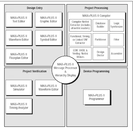
Using a sophisticated computer aided design (CAD) software tool such as Altera’s
Multiple Array MatriX Programmable Logic User System (MAX+PLUS II), one can design
complex logic circuits such as the MIPS Processor. MAX+PLUS II offers a graphical user
methods for hierarchical design, powerful logic synthesis, timing-driven compilation,
partitioning, function and timing simulation, linked multi-device simulation, timing analysis,
automatic error location, and device programming and verification. Figure 1.7 shows how the
eleven integrated applications are grouped within MAX+PLUS II. The industry-standard design
language VHDL can be used in the MAX+PLUS II text editor to specify logic circuits including
the various components of the single-cycle and pipelined implementation of the MIPS processor.
Once the VHDL code is complete, MAX+PLUS II will translate upon request, optimize,
synthesize and save a text-based representation of a logic diagram. MAX+PLUS II can then fit
the circuit design onto the device’s logic elements and programmable interconnection network.
This allows the designer to perform a simulation using actual logic gate and interconnect timing
delays based on the assigned PLD. The final step is to download and configure the actual PLD
with the program and perform a hardware verification of the design.
2 R
ELATED
W
ORK
In the early 1990s, Professors H. B. Diab and I. Demashkieh from the American
University of Beirut in Beirut, Lebanon where the first to determine new methods of effective
microprocessor architecture education. In their paper
A Re-configurable Microprocessor
Teaching Tool
[8], they introduced an interactive, flexible, user-friendly software package to
help describe how an 8-bit CPU functions internally as the master of a micro-computer system.
The tool aids students by providing a graphical step by step animation of how the CPU works.
This tool simulates the CPU control logic, internal registers, buses and memory contents at every
clock edge. It can also simulate read and write cycle to/from memory and input/output devices.
The software package also includes an assembler allowing students to choose either assembly
code or machine code to run on the microprocessor, much like the newer SPIM simulator. Such
a tool enables students to see first hand how the different parts of the microprocessor interact and
how they combine into a working microprocessor, thus introducing one of the first
simulator-based approaches to microprocessor instruction.
More recently in early 2000, Jan Gray, a software developer from Gray Research,
initiated a strong campaign to use FPGA implementations in microprocessor instruction [9].
However, his work demonstrates optimizing CPU design to achieve a cost-effective integrated
computer system in an FPGA.
One goal of this project is to use the ideas presented in [8] to create an effective method
to teach microprocessor design by giving the computer architecture students a complete hands-on
experience with hardware-software integration, a technique that several other universities have
from Cornell University where in 1998 the EE 475 architecture class projects included a VHDL
design and FGPA verification of a simple processor [14]. Most recently, in 2001 at Hiroshima
City University located in Japan it is reported that within a 15 week time period, 7 out of 39
junior students succeeded in implementing hardware description language (HDL) descriptions of
a superscalar RISC processor onto an FPGA. In 2002 in the same 15 week time period, 14 out of
47 junior students implemented varieties of superscalar CISC/RISC processor within an FPGA
[15].
3 FPGA I
MPLEMENTATION OF THE
MIPS P
ROCESSOR
The main task of this project is to implement a single-cycle and pipelined representation
of the MIPS processor onto an FPGA so that it models the processor presented in Chapters 5 and
6 of the book
Computer Organization and Design – The Hardware/Software Interface
by David
A. Patterson and John L. Hennessy [1]. The Altera UP2 Development Board shown in Figure
3.1 was chosen to implement the VHDL design. The development board features one
EPM7128S PLD and one FLEX10K70 FPGA. Each device has the following resources: a JTAG
chain connection for the ByteBlaster II cable (used to program the device), two push-button
switches, dual-digit seven-segment displays, and on-board oscillator (25.175 MHz). The
EPM7128S device also has the following resources available to it: a socket-mounted 84-pin
PLCC package, signal pins that are accessible via female headers, two octal dual inline package
(DIP) switches, 16 LEDs, expansion port with 42 input/output pins and the dedicated global
CLR, OE1, and OE2/GCLK2 pins. The FLEX10K70 device has the additional resources
available to it: a socket for an EPC1 configuration device, one octal DIP switch, VGA video
seven global pins. Altera MAX+PLUS II 10.2 Baseline was the CAD design software chosen
for the design platform.
Figure 3.1 Altera UP2 Development Board [10]
3.1 T
HE
MIPS I
NSTRUCTION
S
ET
A
RCHITECTURE
As mentioned before MIPS is a RISC microprocessor architecture. The MIPS
Architecture defines thirty-two, 32-bit general purpose registers (GPRs). Register $r0 is
hard-wired and always contains the value zero. The CPU uses byte addressing for word accesses and
must be aligned on a byte boundary divisible by four (0, 4, 8, …). MIPS only has three
instruction types: I-type is used for the Load and Stores instructions, R-type is used for
Arithmetic instructions, and J-type is used for the Jump instructions as shown in Figure 3.2.
Table 3.1 provides a description of each of the fields used in the three different instruction types.
MIPS is a load/store architecture, meaning that all operations are performed on operands
held in the processor registers and the main memory can only be accessed through the load and
store instructions (e.g lw, sw). A load instruction loads a value from memory into a register. A
the sum of the offset value in the address/immediate field and the base register in the $rs field to
address the memory. Arithmetic instructions or R-type include: ALU Immediate (e.g. addi),
three-operand (e.g. add, and, slt), and shift instructions (e.g. sll, srl). The J-type instructions are
used for jump instructions (e.g. j). Branch instructions (e.g. beq, bne) are I-type instructions
which use the addition of an offset value from the current address in the address/immediate field
along with the program counter (PC) to compute the branch target address; this is considered
PC-relative addressing. Table 3.2 shows a summary of the core MIPS instructions.
Table 3.1 MIPS Instruction Fields [11]
Instruction Symbol Format
Example
Meaning
Comments
Add add R add $r1, $r2, $r3 $r1 = $r2 + $r3 overflow detectedAdd
Immediate addi I addi $r1, $r2, 100 $r1 = $r2 + 100 plus constant Add
Unsigned addu R addu $r1, $r2, $r3 $r1 = $r2 + $r3
overflow undetected
Subtract sub R sub $r1, $r2, $r3 $r1 = $r2 - $r3 overflow detected Subtract
Unsigned subu R subu $r1, $r2, $r3 $r1 = $r2 - $r3
overflow undetected
And and R and $r1, $r2, $r3 $r1 = $r2 & $r3 bitwise logical and
Or or R Or $r1, $r2, $r3 $r1 = $r2 | $r3 bitwise logical or
Shift Left
Logical sll R sll $r1, $r2, 10 $r1 = $r2 << 10
shift left by constant
Shift Right Logical
srl R srl $r1, $r2, 10 $r1 = $r2 >> 10 shift right by constant
Set Less
Than slt R slt $r1, $r2, $r3
if ($r2 < $r3) $r1 = 1 else 0
compare less than
Load Word lw I lw $r1, 100($r2) $r1 = mem($r2 + 100) from mem to load word reg
Store Word sw I sw $r1, 100($r2) mem($r2 + 100) = $r1 from reg to store word mem Branch on
Equal beq I beq $r1, $r2, 25
if ($r1 = $r2) goto
PC + 4 + 100 equal test Branch on
Not Equal bne I bne $r1, $r2, 25
if ($r1 != $r2) goto PC + 4 + 100
not equal test
Jump j J j 100 goto 400 jump to target
address
Table 3.2 MIPS Core Instructions
3.2 MIPS S
INGLE
-C
YCLE
P
ROCESSOR
The MIPS single-cycle processor performs the tasks of instruction fetch, instruction
decode, execution, memory access and write-back all in one clock cycle. First the PC value is
used as an address to index the instruction memory which supplies a 32-bit value of the next
instruction to be executed. This instruction is then divided into the different fields shown in
Table 3.1. The instructions opcode field bits [31-26] are sent to a control unit to determine the
to be asserted and what function the ALU is to perform, thus decoding the instruction. The
instruction register address fields $rs bits [25 - 21], $rt bits [20 - 16], and $rd bits[15-11] are used
to address the register file. The register file supports two independent register reads and one
register write in one clock cycle. The register file reads in the requested addresses and outputs
the data values contained in these registers. These data values can then be operated on by the
ALU whose operation is determined by the control unit to either compute a memory address (e.g.
load or store), compute an arithmetic result (e.g. add, and or slt), or perform a compare (e.g.
branch). If the instruction decoded is arithmetic, the ALU result must be written to a register. If
the instruction decoded is a load or a store, the ALU result is then used to address the data
memory. The final step writes the ALU result or memory value back to the register file.
3.3 MIPS S
INGLE
-C
YCLE
P
ROCESSOR
VHDL I
MPLEMENTATION
The initial task of this project was to implement in VHDL the MIPS single-cycle
processor using Altera MAX+PLUS II Text Editor to model the processor developed in [1]. A
good VHDL reference and tutorial can be found in the appendices to the book
Fundamentals of
Digital Logic with VHDL Design
by Stephen Brown and Zvonko Vranesic [12]. The
IEEE
Standard VHDL Language Reference Manual
[13], also helped in the overall design of the
VHDL implementation. The first part of the design was to analyze the single-cycle datapath and
take note of the major function units and their respective connections.
The MIPS implementation as with all processors, consists of two main types of logic
elements: combinational and sequential elements. Combinational elements are elements that
operate on data values, meaning that their outputs depend on the current inputs. Such elements
in the MIPS implementation include the arithmetic logic unit (ALU) and adder. Sequential
elements are elements that contain and hold a state. Each state element has at least two inputs
and one output. The two inputs are the data value to be written and a clock signal. The output
signal provides the data values that were written in an earlier clock cycle. State elements in the
MIPS implementation include the Register File, Instruction Memory, and Data Memory as seen
in Figure 3.3. While many of logic units are straightforward to design and implement in VHDL,
considerable effort was needed to implement the state elements.
It was determined that the full 32-bit version of the MIPS architecture would not fit onto
the chosen FLEX10K70 FPGA. The FLEX10K70 device includes nine embedded array blocks
(EABs) each providing only 2,048 bits of memory for a total of 2 KB memory space. The full
32-bit version of MIPS requires no less than twelve EABs to support the processor’s register file,
width was reduced to 8-bit while still maintaining a full 32-bit instruction. This new design
allows us to implement all of the processor’s state elements using six EABs, which can be
handled by the FLEX10K70 FPGA device. Even though the data width was reduced, the design
has minimal VHDL source modifications from the full 32-bit version, thus not impacting the
instructional value of the MIPS VHDL model.
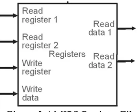
With our new design, the register file is implemented to hold thirty-two, 8-bit general
purpose registers amounting to 32 bytes of memory space. This easily fits into one 256 x 8 EAB
within the FPGA. The full 32-bit version of MIPS will require combining four 256 x 8 EABs to
implement the register file. The register file has two read and one write input ports, meaning that
during one clock cycle, the processor must be able to read two independent data values and write
a separate value into the register file. Figure 3.4 shows the MIPS register file. The register file
was implemented in VHDL by declaring it as a one-dimensional array of 32 elements or registers
each 8-bits wide. (e.g.
TYPE register_file IS ARRAY (0 TO 31) OF STD_LOGIC_VECTOR (7 DOWNTO 0)
)
By declaring the register file as a one-dimensional array, the requested register address would
need to be converted into an integer to index the register file.(e.g.
Read_Data_1 <= register_file (
CONV_INTEGER (read_register_address1 (4 DOWNTO 0))) )
Finally, to save from having to load each
register with a value, the registers get initialized to their respective register number when the
Reset signal is asserted. (e.g. $r1 = 1, $r2 = 2, etc.)
Altera MAX+PLUS II is packaged with a Library of Parameterized Modules (LPM) that
allow one to implement RAM and ROM memory in Altera supported PLD devices. With our
design this library was used to declare the instruction memory as a read only memory (ROM)
and the data memory as a random access memory (RAM). Using the lpm_rom component from
the LPM Library, the Instruction memory is declared as a ROM and the following parameters are
set: the width of the output data port parameter lpm_width is set to 32-bits, the width of the
address port parameter lpm_widthad is set to 8-bits, and the parameter lpm_file is used to
declare a memory initialization file (.mif) that contains ROM initialization data. This allows us
to set the indexed address data width to 8-bits, the instruction output to 32-bits wide, and enables
us to initialize the ROM with the desired MIPS program to test the MIPS processor
implementation. With these settings, four 256 x 8 EABs are required to implement the
instruction memory. An example of the MIPS instruction memory can be seen in Figure 3.5 and
the VHDL code implementation can be seen in Figure 3.6.
Figure 3.5 MIPS Instruction Memory
Figure 3.6 VHDL – MIPS Instruction Memory
The data memory is declared using the lpm_ram_dq component of the LPM library. This
component is chosen because it requires that the memory address to stabilize before allowing the
write enable to be asserted high. The input Address width (lpm_widthad) and the Read Data
Instr_Memory: LPM_ROM GENERIC MAP(
LPM_WIDTH => 32,
LPM_WIDTHAD => 8,
LPM_FILE => "instruction_memory.mif",
LPM_OUTDATA => "UNREGISTERED", LPM_ADDRESS_CONTROL => "UNREGISTERED") PORT MAP (
address => PC,
output width (lpm_width) are both declared as 8-bit wide, in lieu of our altered design. Using
these settings allows us to use one 256 x 8 EAB instead of the 4 combined EABs required for the
full 32-bit version of MIPS. An example of the MIPS data memory can be seen in Figure 3.7
and the VHDL code implementation can be seen in Figure 3.8.
Figure 3.7 MIPS Data Memory
Data_Memory : LPM_RAM_DQ
GENERIC
MAP(
LPM_WIDTH
=>
8,
LPM_WIDTHAD
=>
8,
LPM_FILE
=>
"data_memory.mif",
LPM_INDATA
=>
"REGISTERED",
LPM_ADDRESS_CONTROL
=>
"UNREGISTERED",
LPM_OUTDATA
=>
"UNREGISTERED")
PORT
MAP(
inclock =>
Clock,
data
=>
Write_Data,
address =>
Address,
we
=>
LPM_WRITE,
q
=>
Read_Data);
Figure 3.8. VHDL – MIPS Data Memory
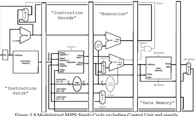
Once we determined how to declare the state elements of the MIPS processor it was time
to implement the rest of the logic devices in VHDL. Because the final task is to pipeline the
implementation into the five different VHDL modules to be fully utilized later in the pipelined
implementation of the MIPS processor. The five modules are: Instruction Fetch, Instruction
Decode, Control Unit, Execution, and Data Memory as shown in Figure 3.9.
Figure 3.9 Modularized MIPS Single Cycle excluding Control Unit and signals.
With the decision to use five different modules to implement the single-cycle MIPS processor,
the VHDL design becomes a two-level hierarchy. The top-level of the hierarchy is a structural
VHDL file that connects the all five components of the single-cycle implementation, while the
bottom-level contains the behavioral VHDL models of the five different components. Appendix
C contains the top-level structural VHDL code for the MIPS single-cycle processor.
3.3.1 I
NSTRUCTION
F
ETCH
U
NIT
The function of the instruction fetch unit is to obtain an instruction from the instruction
shown in Figure 3.10. Since this design uses an 8-bit data width we had to implement byte
addressing to access the registers and word address to access the instruction memory. The
instruction fetch component contains the following logic elements that are implemented in
VHDL: 8-bit program counter (PC) register, an adder to increment the PC by four, the
instruction memory, a multiplexor, and an AND gate used to select the value of the next PC.
Appendix C contains the VHDL code used to create the instruction fetch unit of the MIPS
single-cycle processor.
Figure 3.10 MIPS Instruction Fetch Unit
3.3.2 I
NSTRUCTION
D
ECODE
U
NIT
The main function of the instruction decode unit is to use the 32-bit instruction provided
from the previous instruction fetch unit to index the register file and obtain the register data
values as seen in Figure 3.11. This unit also sign extends instruction bits [15 - 0] to 32-bit.
However with our design of 8-bit data width, our implementation uses the instruction bits [7 – 0]
bits instead of sign extending the value. The logic elements to be implemented in VHDL include
several multiplexors and the register file, that was described earlier. Appendix C contains the
Figure 3.11 MIPS Instruction Decode Unit
3.3.3 T
HE
C
ONTROL
U
NIT
The control unit of the MIPS single-cycle processor examines the instruction opcode bits
[31 – 26] and decodes the instruction to generate nine control signals to be used in the additional
modules as shown in Figure 3.12. The RegDst control signal determines which register is
written to the register file. The Jump control signal selects the jump address to be sent to the PC.
The Branch control signal is used to select the branch address to be sent to the PC. The
MemRead control signal is asserted during a load instruction when the data memory is read to
load a register with its memory contents. The MemtoReg control signal determines if the ALU
result or the data memory output is written to the register file. The ALUOp control signals
determine the function the ALU performs. (e.g. and, or, add, sbu, slt) The MemWrite control
signal is asserted when during a store instruction when a registers value is stored in the data
memory. The ALUSrc control signal determines if the ALU second operand comes from the
needs to be written. Table 3.3 shows the control signal values from the instruction decoded.
Appendix C contains the VHDL code for the MIPS single-cycle control unit.
Figure 3.12 MIPS Control Unit
Instruction RegDst ALUSrc MemtoReg RegWrite MemRead MemWrite Branch ALUOp1 ALUOp0
R-type
1
0
0
1
0
0
0
1
0
lw
0
1
1
1
1
0
0
0
0
sw
X
1
X
0
0
1
0
0
0
beq
X
0
X
0
0
0
1
0
1
Table 3.3 MIPS Control Signals
3.3.4 E
XECUTION
U
NIT
The execution unit of the MIPS processor contains the arithmetic logic unit (ALU) which
performs the operation determined by the ALUop signal. The branch address is calculated by
adding the PC+4 to the sign extended immediate field shifted left 2 bits by a separate adder. The
logic elements to be implemented in VHDL include a multiplexor, an adder, the ALU and the
ALU control as shown in Figure 3.9 Appendix C contains the VHDL code used to create the
F
IGURE
3.13 MIPS E
XECUTION
U
NIT
3.3.5 D
ATA
M
EMORY
U
NIT
The data memory unit is only accessed by the load and store instructions. The load
instruction asserts the MemRead signal and uses the ALU Result value as an address to index the
data memory. The read output data is then subsequently written into the register file. A store
instruction asserts the MemWrite signal and writes the data value previously read from a register
into the computed memory address. The VHDL implementation of the data memory was
described earlier. Figure 3.14 shows the signals used by the memory unit to access the data
memory. Appendix C contains the complete VHDL code used to create the memory state of the
MIPS single-cycle processor. Appendix D shows an example of MIPS single-cycle being
Figure 3.14 MIPS Data Memory Unit
3.4 MIPS P
IPELINED
P
ROCESSOR
VHDL I
MPLEMENTATION
Once the MIPS single-cycle VHDL implementation was completed, our next task was to
pipeline the MIPS processor. Pipelining, a standard feature in RISC processors, is a technique
used to improve both clock speed and overall performance. Pipelining allows a processor to
work on different steps of the instruction at the same time, thus more instruction can be executed
in a shorter period of time. For example in the VHDL MIPS single-cycle implementation above,
the datapath is divided into different modules, where each module must wait for the previous one
to finish before it can execute, thereby completing one instruction in one long clock cycle.
When the MIPS processor is pipelined, during a single clock cycle each one of those modules or
stages is in use at exactly the same time executing on different instructions in parallel. Figure
3.15 shows an example of a MIPS single-cycle non-pipelined (a.) versus a MIPS pipelined
implementation (b.). The pipelined implementation executes faster, keep in mind that both
Instruction
fetch Reg ALU Data access Reg
8 ns Instructionfetch Reg ALU Data
access Reg
8 ns Insfterutcchtion
8ns Time
lw$1,100($0)
lw$2,200($0)
lw$3,300($0)
2 4 6 8 10 12 14 16 18
2 4 6 8 10 12 14
...
Program
execution
order
(ininstructions)
Instruction
fetch Reg ALU
Data access Reg
Time
lw$1,100($0)
lw$2,200($0)
lw$3,300($0)
2ns Insftreutcchtion Reg ALU accessData Reg
2ns Instructionfetch Reg ALU accessData Reg
2 ns 2 ns 2 ns 2 ns 2 ns rogram
xecution
order
(ininstructions)
a.)
b.)
P eFigure 3.15. Single-cycle non-pipelined (a) vs. pipelined execution (b)
The MIPS pipelined processor involves five steps, the division of an instruction into five
stages implies a five-stage pipeline:
1. Instruction Fetch (IF): fetching the instruction from the memory
2. Instruction Decode (ID): reading the registers and decoding the instruction
3. Execution (EX): executing an operation or calculating an address
4. Data Memory (MEM): accessing the data memory
5. Write Back (WB): writing the result into a register.
The key to pipelining the single-cycle implementation of the MIPS processor is the introduction
of pipeline registers that are used to separate the datapath into the five sections IF, ID, EX, MEM
and WB. Pipeline registers are used to store the values used by an instruction as it proceeds
through the subsequent stages. The MIPS pipelined registers are labeled according to the stages
they separate. (e.g. IF/ID, ID/EX, EX/MEM, MEM/WB) Figure 3.16 shows and example of a
MEM
WB
PC
Instruction memory Address
I n s t r u c t i o n
Instruction [20–16]
MemtoReg ALUOp Branch RegDst ALUSrc 4
16 32
Instruction [15–0]
0 0
Registers Write register Write data
Read data 1
Read data 2 Read
register1 Read register2
Sign extend M u x 1
Write data
Read
data M u x 1
ALU control RegWrite
MemRead
Instruction [15–11]
6
IF/ID ID/EX EX/MEM MEM/WB
MemWrite
Address Data memory
PCSrc
Zero
AddresultAdd
Shift left 2 ALU result ALU Zero
Add 0 1 M u x 0 1 M u x
IF
ID
EX
Figure 3.16 MIPS Pipelined Processor Datapath [1]
To implement the MIPS pipelined processor, pipeline registers are placed into the
corresponding VHDL modules that generate the input to the particular pipeline register. For
example, the Instruction Fetch component will generate the 32-bit instruction and the PC+4
value and store them into the IF/ID pipeline register. When that instruction moves to the
Instruction Decode stages it extracts those saved values from the IF/ID pipeline register.
Appendix F contains the complete VHDL code used to implement the MIPS pipelined processor
data path. Appendices G shows an example of MIPS processor pipelined being simulated.
3.4.1 P
IPELINE
H
AZARDS
Pipelining the MIPS processor introduces events called hazards, which prevent the next
types of possible hazards include structural, data and control hazards. Structural hazards arise
when the hardware cannot support the instructions that are ready to execute during the same
clock cycle. Fortunately, MIPS is designed to be pipelined thus no structural hazards exist.
However, if the MIPS processor had been designed with one memory to be shared between both
instructions and data, then a structural hazard would occur.
Data hazards arise when an instruction depends on the result of a previous instruction in a
way that is exposed by the overlapping of the instructions in the pipeline, thus causing the
pipeline to stall until the results are made available. One solution to this type of data hazard is
called forwarding, which supplies the resulting operand to the dependant instruction as soon it
has been computed. Figures 3.17 shows an example of pipelined data dependencies and Figure
3.18 shows how these dependencies are resolved using a forwarding unit. Appendix I MIPS
Pipelined – Data Hazards and Forwarding Simulation, simulates this exact example.
IM Reg
I M Reg
C C 1 C C 2 CC 3 CC 4 CC 5 CC 6
Time(inclockcycles)
sub , $1, $3 Program
e x e c u t i o n
order
( i n in s t r u c t i o n s )
a n d $ 1 2 , $ 5
IM DM Reg
IM DM R e g
IM D M Reg
CC 7 C C 8 CC 9
10 10 10 10 10/– 20 – 20 – 20 –20 – 20
or $13, $6,
a d d $ 1 4 ,
s w $ 1 5 , 1 0 0 Valueof
register $2:
DM
DM
$2
$2,
Reg
$2
$2, $2
($2)
Reg
Reg
Reg Reg
IM Reg
IM Reg
CC1 CC2 CC 3 CC 4 CC 5 CC 6 Time(inclockcycles)
sub $1, $3 Program
executionorder
(ininstructions)
and$12, $5
IM DM Reg
IM DM Reg
IM DM Reg
CC 7 CC8 CC 9 10 10 10 10 10/– 20 – 20 – 20 –20 – 20
or$13,$6,
add$14,
sw $15, 100 Valueofregister$2:
DM
X X X – 20 X X X X X
ValueofEX/MEM:
X X X X – 20 X X X X
ValueofMEM/WB:
DM
$2,
$2,
Reg
$2
$2,$2
($2)
Reg
Reg
Reg Reg
Figure 3.18 Pipelined Data Dependencies Resolved with Forwarding [1]
While forwarding is an exceptional solution to data hazards it does not resolve all of
them. One instance is when an instruction attempts to read a register value that is going to be
supplied by a previous load instruction that writes the same register, called a load-use hazard.
At the same time the load instruction is reading data from memory, the subsequent instruction
executing in the execution stage with the wrong data value. The only solution here is to stall the
pipeline and wait for the correct data value being used as an operand. In order to detect such
hazards, MIPS introduces a Hazard Detection Unit during the instruction decode stage so that it
can stall the pipeline between a load instruction and the immediate instruction attempting to use
the same register. Figure 3.19 show an example where the forwarding using can not resolve a
data dependence, the solution is to this type of data hazard it to insert a stall shown in Figure
3.20 as a bubble. Appendix K MIPS Pipelined – Data Hazards and Stalls Simulation, shows this
IM
Reg Reg
IM
CC1 CC2 CC 3 CC 4 CC 5 CC 6 Time (in clock cycles)
lw
20($1) Program execution order (ininstructions)
and $5
IM DM Reg
IM DM Reg
IM DM Reg
CC 7 CC 8 CC9
or$8, $6
add$9,
slt $1, $6, $7
DM
DM Reg $2,
$4,$2,
Reg $2,
$4,$2
Reg
Reg
Reg
$2,
$4,$2,
$2,
$4,$2
Reg Reg Reg Reg Reg Reg
Figure 3.19 Pipelined Data Dependencies Requiring Stall [1]
lw 20($1) Program execution order (ininstructions)
and $5
or$8, $6
add$9,
slt $1, $6, $7 IM
Reg Reg
IM DM
CC1 CC2 CC 3 CC 4 CC 5 CC 6 Time(inclockcycles)
IM DM Reg
IM
IM DM Reg
IM DM Reg
CC 7 CC 8 CC9 CC10
DM
bubble
Figure 3.20 Pipelined Data Dependencies Resolved with Stall [1]
The last type of hazard is a control hazard also known as a branch hazard. These hazards
occur when there is a need to make a decision based on the results of one instruction while other
instructions continue executing. For example, a branch on equal instruction will branch to a
non-sequential part of the instruction memory if the two register values compared are equal. While
the register values are compared, other instructions continue to be fetched and decoded. If the
branch is taken, the wrong instructions are fetched into the pipeline and must somehow be
discarded. Figure 3.21 shows three instructions that need to be discarded after it is determined
the branch instruction will be taken. A common solution to these hazards is to continue
taken, the instructions that were fetched and decoded must be discarded which can be achieved
by flushing some of the pipeline registers. Flushing means that all values stored in the pipeline
registers are discarded or reset. However in order to reduce the branch hazard to 1 clock cycle,
the branch decision is moved from the memory pipeline stage to the instruction decode stage.
By simply comparing the registers fetch it can be determined if a branch is to be taken or not.
Appendix M MIPS Pipelined – Branch Hazard Simulation, shows an example of a branch
instruction being taken, flushing the IF/ID pipeline register, and loading the new instruction
determined from the branch address.
Reg Reg
CC1 Time(inclockcycles)
40 beq $1, $3, 7 Program
execution
order
(in instructions)
IM Reg
IM DM
IM DM
IM DM
DM
DM Reg
Reg Reg
Reg
Reg
Reg 44and$12,$2, $5
48or$13,$6,$2
52add$14,$2, $2
72lw$4,50($7)
CC 2 CC 3 CC 4 CC 5 CC 6 CC 7 CC8 CC9
Reg
IM
Figure 3.21 Pipelined Branch Instruction [1]
Appendix F MIPS Pipelined – VHDL Code, contains the complete VHDL code used to
implement the MIPS pipelined processor including the solutions to resolve data and branch
hazards. Appendices I, K, and M show example of MIPS pipelined being simulated. Appendix
O MIPS Pipelined Final Dathpath and Control, shows the complete datapath and control that was
3.5 H
ARDWARE
I
MPLEMENTATION
Once the VHDL code was simulated and all operations were verified using Altera
MAX+PLUS II Waveform Editor and Simulator, the design would then need to be prepared for
the hardware implementation on to the Altera UP2 Development board. Preparing the VHDL
design involves assigning VHDL code signals to device pins found on the UP2 board. For
example the reset signal was assigned to an on-board push button (PB) switch allowing us to
manually reset the processor. Table 3.3 shows the UP2 Board FLEX10K70 I/O pin
assignments.
Pin Name
Pin Pin Type Function
Clock
91
Input
25.175 MHz System Clock
PB1 28
Input
Push-button
1
PB2 29
Input
Push-button
2
FLEX_switch_1 41
Input
FLEX DIP Switch 1
FLEX_switch_2 40
Input
FLEX DIP Switch 2
FLEX_switch_3 39
Input
FLEX DIP Switch 3
FLEX_switch_4 38
Input
FLEX DIP Switch 4
FLEX_switch_5 36
Input
FLEX DIP Switch 5
FLEX_switch_6 35
Input
FLEX DIP Switch 6
FLEX_switch_7 34
Input
FLEX DIP Switch 7
FLEX_switch_8 33
Input
FLEX DIP Switch 8
MSD_dp
14
Output
Most Significant Digit of Seven Segment Display
Decimal Point Segment
MSD_a
6
Output
MSD Segment a
MSD_b
7
Output
MSD Segment b
MSD_c
8
Output
MSD Segment c
MSD_d
9
Output
MSD Segment d
MSD_e
11
Output
MSD Segment e
MSD_f
12
Output
MSD Segment f
MSD_g
13
Output
MSD Segment g
LSD_dp
25
Output
Least Significant Digit of Seven Segment Display
Decimal Point Segment
LSD_a
17
Output
LSD Segment a
LSD_b
18
Output
LSD Segment b
LSD_c
19
Output
LSD Segment c
LSD_d
20
Output
LSD Segment d
LSD_e
21
Output
LSD Segment e
LSD_f
23
Output
LSD Segment f
LSD_g
24
Output
LSD Segment g
Blue
238
Output
VGA Video Signal – Blue Video Data
Green
237
Output
VGA Video Signal – Green Video Data
Red
236
Output
VGA Video Signal – Red Video Data
Horizontal_sync 240
Output
VGA Video Signal – Horizontal Synchronization
Vertical_sync
239
Output
VGA Video Signal – Vertical Synchronization
Programming or downloading the design to a UP2 board requires setting on-board
jumpers that indicate which PLD device to program. The jumpers indicate if you want to
program only the EMP7128S device, program only the FLEX10K70 device, program both
devices or connect multiple UP2 boards together in a chain. The Altera
University Program
UP2 Development Kit User Guide
[10], explains how to setup the jumpers to program the
desired device. Once the jumpers are set the MAX+PLUS II software must be setup to configure
the devices via a JTAG chain. The JTAG uses boundary-scan technology that allows one to
perform downloading, debugging and diagnostics on a system through a small number of
dedicated test pins. Once the software is properly setup, the design can then easily be
downloaded using the ByteBlaster II download cable, a cable that provides a hardware interface
to the UP2 via JTAG connector and a connection to the computer running MAX+PLUS II via a
standard parallel port. For complete instructions on setting up the MAX+PLUS II software to
program the devices via the ByteBlaster II download cable please see the
ByteBlaster MV
Parallel Port Download Cable Data Sheet
by Altera [16]. By choosing to program and
configure the FLEX10K70 FPGA device our design of the MIPS single-cycle processor easily fit
onto this device. The VGA video output display on the UP2 board was used to display some
hexadecimal output values of the major functional processor units and the two seven-segment
display were configured to display the hexadecimal output values of the current program counter
(PC). Finally one on-board push button switch was configured to used as the global reset signal
and the other push button switch was configured to simulate a clock cycle when depressed. Both
VHDL implementations of the MIPS single-cycle and pipelined processors were downloaded
and used to configure the Altera FLEX10K70 device with plenty of room and resources to spare.
Processor
Pins
Logic Cells Memory Bits EABs
Single-cycle 19/189
1238/3744 9472/18432 5/9
Pipelined 19/189
1423/3744
11240/18432 6/9
Table 3.5 FLEX10K70 Resource Utilization Table
4 R
ESULTS AND
D
ISCUSSION
The work presented in this paper describes a functional FPGA implementation design of
a MIPS single-cycle and pipelined processor designed using VHDL. The project was to model
Chapters 5 and 6 from the widely used book
Computer Organization and Design – The
Hardware/Software Interface
by David A. Patterson and John L. Hennessy, to help the computer
architecture students gain a better understanding of the MIPS processor. The VHDL designs of
the MIPS processor were all simulated to ensure that the processors were functional and operated
just as described by Patterson and Hennessy. The Appendices D, G, I, K, and M presented in
this paper show some specific examples presented by Patterson and Hennessy being simulated
by the VHDL designs. The appendices first show the instruction memory initialization file,
which is used to fill the instruction memory with the instructions to be executed as seen in Figure
4.1. The first column of numbers is the hexadecimal memory address of the instructions, which
are indexed by the program counter (PC). The second column of characters is the actual 32-bit
instruction represented using hexadecimal numbers. The third column of numbers is the PC
value used to index the instruction memory to retrieve an instruction. The next four columns are
the MIPS instruction’s mnemonic description. Finally last columns are the pseudo instructions
using the actual values used during the simulation.
--Initialized Instruction Memory --PC Instruction
00: 8C2A0014; --00: LW $10, 20 ($1) $10 (0x0A) = MEM(0x01+0x14) = MEM(0x15) = 0x15 01: 00435822; --04: SUB $11, $2, $3 $11 (0x0B) = 0x02 - 0x03 = 0d-1 = 0XFF 02: 00856024; --08: AND $12, $4, $5 $12 (0x0C) = 0x04 AND 0x05 = 0d 4 = 0x04 03: 00C76825; --0C: OR $13, $6, $7 $13 (0x0D) = 0x06 OR 0x07 = 0d 7 = 0x07 04: 01097020; --10: ADD $14, $8, $9 $14 (0x0E) = 0x08 + 0x09 = 0d17 = 0x11
Figure 4.2 shows a screenshot of the Altera MAX+PLUS II Waveform Editor and Simulator
results for the instructions shown in Figure 4.1. The first two rows depict the global clock and
reset signals. The following rows are executed during the Instruction Fetch stage of the MIPS
pipelined processor. The signals are the PC value, used to index the instruction memory and the
32-bit instruction that was index out of the instruction memory. Please note that these values
correspond to those shown in Figure 4.1. The next group of signals are executed during the
Instruction Decode stage of the pipelined processor. These values depict the register values
indexed from the register file and various other signals used during hazard detection. The third
group of signals are executed during the Execution stage of the pipelined processor. These
signals show the two values fed into the ALU and the corresponding result. The following group
of signals depict the memory stage of the pipelined processor. These signals are only used for
the load and store instructions to access the data memory. In this example we can see that the
memory address 0x15 was calculate during the execution unit is used to index or read the data
memory and retrieve the value 0x15. In this specific case the data memory for address 0x15 was
initialized with the same value 0x15. Finally the last group of signals are executed during the
write back stage of the pipelined processor. The RegWrite_out signal tells us when the register
file is going to be written. The WriteRegister__out signal is the actual register to be written and
Figure 4.2 Altera MAX+PLUS II Waveform Editor and Simulator Screenshot
Every simulation shown in the appendices come accompanied by results obtained from
the SPIM Simulator which was used to validate the results obtained by the Altera MAX+PLUS
II Simulator. SPIM is a software simulator that runs programs written for the MIPS processor, it
can read and write MIPS assembly language files to simulate programs. An example of the
SPIM Simulator registers and console are shown in Figure 4.3. Part of SPIMs output is the value
of the thirty two general purpose registers available in the MIPS instruction set architecture
shown as R0 – R31. MIPS architecture developed a convention and suggested guidelines on
how these register showed be used, those are the values seen in the parenthesis. For example
registers $a0 - $a3 are used to pass arguments to routines, $t0 - $t9 are temporary registers and
$s0 - $s7 hold long-lived values. The second part of the output shown is the Console. The
console is SPIMs that displays all characters the program writes as output. In this example I’ve
Using the MIPS register convention I have used the registers $s0 - $s7 to save all results. The
results shown in the console can be used to validate the results obtained from the Altera
MAX+PLUS II Simulator.
Registers
=========================
PC = 00000000 EPC = 00000000 Cause = 00000000 BadVAddr= 00000000 Status = 00000000 HI = 00000000 LO = 00000000
General Registers
R0 (r0) = 00000000 R8 (t0) = 00000000 R16 (s0) = 00000015 R24 (t8) = 00000008 R1 (at) = 10010000 R9 (t1) = 00000000 R17 (s1) = ffffffff R25 (t9) = 00000009 R2 (v0) = 0000000a R10 (t2) = 00000002 R18 (s2) = 00000004 R26 (k0) = 00000000 R3 (v1) = 00000000 R11 (t3) = 00000003 R19 (s3) = 00000007 R27 (k1) = 00000000 R4 (a0) = 10010093 R12 (t4) = 00000004 R20 (s4) = 00000011 R28 (gp) = 10008000 R5 (a1) = 00000000 R13 (t5) = 00000005 R21 (s5) = 00000000 R29 (sp) = 7fffe850 R6 (a2) = 7fffe858 R14 (t6) = 00000006 R22 (s6) = 00000000 R30 (s8) = 00000000 R7 (a3) = 00000000 R15 (t7) = 00000007 R23 (s7) = 00000000 R31 (ra) = 00000000 Console
=========================
00: $s0 = 0x15 = 0d21 = 0x00000015 01: $s1 = 0x02 SUB 0x03 = 0d-1 = 0xffffffff 02: $s2 = 0x04 AND 0x05 = 0d4 = 0x00000004 03: $s3 = 0x06 OR 0x07 = 0d7 = 0x00000007 04: $s4 = 0x08 ADD 0x09 = 0d17 = 0x00000011


![Figure 3.1 Altera UP2 Development Board [10]](https://thumb-us.123doks.com/thumbv2/123dok_es/5882762.154445/16.918.161.769.187.527/figure-altera-up-development-board.webp)
![Table 3.1 MIPS Instruction Fields [11]](https://thumb-us.123doks.com/thumbv2/123dok_es/5882762.154445/17.918.147.770.411.1054/table-mips-instruction-fields.webp)