UNIVERSIDAD DE VALLADOLID
ESCUELA DE INGENIERIAS INDUSTRIALES
GRADO EN INGENIERÍA ELECTRÓNICA INDUSTRIAL Y AUTOMÁTICA
DISEÑO DE UN SENSOR DE TEMPERATURA
IOT PARA LA RED LORA
DESIGN OF IOT TEMPERATURE SENSOR FOR LORA NETWORK
Autor:
Rodríguez Lallana, Mario
Marta Herráez Sánchez
2
Valladolid, Junio de 2018
TFG REALIZADO EN PROGRAMA DE INTERCAMBIOTÍTULO: DESIGN OF IOT TEMPERATURE SENSOR FOR LORA NETWORK / DISEÑO DE UN SENSOR DE TEMPERATURA IOT PARA LA RED LORA
ALUMNO: Mario Rodríguez Lallana FECHA: 07/06/2018
3
Resumen:
El objetivo de este proyecto es implementar una solución válida para un proyecto de IoT basado en un LM35 (sensor de temperatura), que proporciona los datos que se transmitirán a través de una WAN LoRa, y un módulo, el TTGO LoRa Wifi V1. Esté módulo está formado por: el chip ESP32, un OLED controlado por el SSD1306 y un transceptor LoRa controlada por el SX1276.
La transmisión de RF tendrá lugar en la banda de la UE reservada para la tecnología LoRa, 868 MHz. Y los paquetes LoRa WAN serán enviados a un Gateway LoRa que los redirigirá a la nube a nuestra aplicación en línea.
Después de todo, esta aplicación, que se hará en línea con la plataforma
TheThingsNetwork.org, tendrá el deber de gestionar el paquete que recibe decodificarlos y proporcionar un entorno fácil de usar para mostrar estos datos para nosotros, y la
información de la misma.
Palabras clave:
4
Vilnius Gediminas Technical University
Faculty of Electronics
Mario Rodríguez Lallana
Design of IoT temperature sensor for
Lora network
Bachelor`s Thesis
Supervisor: Dainius Udris,
Department of Electrical Engineering
5
Declaration: I hereby declare that this Bachelor’s thesis, my original investigation and achievement, submitted for the Bachelor’s degree at Vilnius Gediminas Technical University has not been submitted for any degree or examination.
Mario Rodríguez Lallana
Date ………...
6
INDEX OF CONTENTS
1. INTRODUCTION. ... 12
1.1. Goals: ... 12
2. ANALYTICAL PART. ... 14
2.1. Structure and characteristics of Lora network. ... 14
2.1.1. LoRa Network architecture ... 14
2.1.3. LoRa MAC layer ... 19
2.2. Lora endpoint realization examples, chipsets and their comparison. ... 26
2.3. Environmental sensors and their data acquisition. ... 28
2.3.1. Humidity and temperature sensor ... 28
2.3.2. HL 69 Soil hygrometer moisture sensor ... 29
2.3.3. Ultrasonic distance sensor HC-SR04 ... 31
2.3.4. Sensor de temperature LM35 ... 34
2.3.5. MMA7361 Accelerometer sensor ... 34
3. DESIGN PART. ... 37
3.1. Sensor selection and requirements for data reading. ... 37
3.2. Functional diagram design. ... 41
3.3. Microcontroller selection. Parameters, connectivity and toolset of ESP32. ... 42
3.3.1. Introduction ... 42
3.3.2. Parameters of ESP32 ... 42
3.3.3. Toolset ... 44
3.4. Lora chip selection. Parameters, connectivity and programming of SX1276. ... 48
3.4.1. Introduction ... 48
3.4.2. Parameters ... 49
3.4.3. Connectivity ... 49
3.4.4. Programming ... 52
3.5. OLED display with SSD1306 controller connection and programming. ... 53
7
3.5.2. Connection ... 54
3.5.3. Programming ... 62
3.6. The schematic diagram design (including internal connections of presented TTGO Lora module). ... 64
3.7. The data reading and transmission flowchart design. ... 65
3.8. The program design using Arduino shield with libraries. ... 67
3.8.1. OLED_LoRa_sender.ino ... 67
3.8.2. Ttgo_abp_lorawan.ino ... 72
3.8.3. Ttgo_abp_lorawan_LM35sensor2.ino ... 82
4. Obtained results and conclusions. ... 84
4.1. Sensor and Data Reading and transformation to digital (ADC) ... 84
4.2. How to use LoRa WAN with TTGO LoRa ESP32 ... 85
4.2.1. Introduction ... 85
4.2.2. Step by step ... 85
4.2.3. Decoding of the data transmitted ... 88
4.2.4. Attaching the sensor ... 89
4.2.5. TheThingsNetwork application ... 96
4.2.6. Two more basic notions of LoRa WAN: ... 100
4.3. Final working test: ... 104
5. CONCLUSIONS. ... 107
6. REFERENCES. ... 108
7. ANEXES. ... 112
7.1. Code ... 112
7.1.1. SSD1306.h library ... 112
7.1.2. Oled_LoRa_sender.ino ... 113
7.1.3. Ttgo_abp_lorawan.ino ... 115
7.1.4. Ttgo_abp_lorawan_LM35sensor2.ino ... 119
7.2. LM35 electrical characteristics ... 124
8
INDEX OF FIGURES
Figure 1 LoRa WAN architecture and devices classes [7] ... 14
Figure 2 LoRa network architecture [6] ... 15
Figure 3 Up-Chirp spread spectrum modulation example in time domain [6] ... 16
Figure 4: example of FSK frequency shift keying. [5] ... 16
Figure 5: example of chirp modulation [5] ... 17
Figure 6: Bandwidth and Sweep rate in the chirp modulation [5]... 17
Figure 7 preamble of a physical frame format [6] ... 18
Figure 8 LoRa WAN Physical Layer Frame Format [7] ... 18
Figure 9: Class A type device transmission [8] ... 21
Figure 10 Class A device timing diagram [8]... 21
Figure 11 Class B type device transmission [8] ... 22
Figure 12 Class b device timing diagram [8] ... 22
Figure 13 Class C type transmission [8] ... 23
Figure 14 Class C device timing diagram [8] ... 23
Figure 15 PHYPayload [7] ... 24
Figure 16MACcommands [7] ... 24
Figure 17 MAC Payload [7] ... 24
Figure 18 detailed FHDR [7] ... 25
Figure 19 MAC payload sizes varying with the frequency [7] ... 25
Figure 20 my network ... 26
Figure 21 DHT11 with his pinout and how to connect it with a controller [12] ... 29
Figure 22 pinout of the controller of the HL69 [13]... 30
Figure 23 Arduino example of how to connect the two parts of this sensor to read data [13] ... 31
Figure 24 pinout of the HC-SR04 [14] ... 31
Figure 25 example of how to read data from the HC-SR04 with an Arduino UNO [14] ... 33
Figure 26 HC-SR04 trigger and echo transmission timing diagram [14]... 33
Figure 27 MMA736 accelerometer sensor [15] ... 34
9
Figure 29 Arduino pin connection example [15] ... 36
Figure 30 Pinout of the LM35 [16] ... 37
Figure 31 Bottom view of LM35 LP package [16] ... 37
Figure 32 basic temperature sensor (2ºC to 150ºC) [16] ... 39
Figure 33 full range centigrade temperature sensor [16] ... 39
Figure 34 Accuracy vs Temperature (Ensured) [16] ... 40
Figure 35 sensor volt input versus the ESP32 adc output. [17] ... 40
Figure 36 Simple Connections Diagram ... 41
Figure 37 Complex Connections Diagram ... 41
Figure 38 ESP 32 block diagram [18] ... 44
Figure 39 Git Gui menu ... 45
Figure 40: execution of get.exe ... 46
Figure 41 new get files ... 46
Figure 42 ESP 32 pinout [20] ... 47
Figure 43 TTGO ESP32 LoRa module V1 [19] ... 48
Figure 44 SX1276 pinout [21] ... 48
Figure 45 SPI timing diagram (SINGLE access) [21] ... 50
Figure 46 SSD1306 controller and OLED display ... 54
Figure 47 SSD1306 controller and OLED display (technical) [23] ... 54
Figure 48 SSD1306 controller connections needed to work with any other device... 55
Figure 49 Block diagram of the SSD1306 OLED dislpay controller [23] ... 56
Figure 50 Communication diagram between a MCU the Seg/Com driver and the OLED display ... 57
Figure 51 GDDRAM pages structure of SSD1306 [23] ... 57
Figure 52 Detailed pages of the SSD1306 [23] ... 58
Figure 53 pinout scheme of the SSD1306 controller [23] ... 59
Figure 54 Master-Slave communication with I2C interface basic diagram [24] ... 60
Figure 55 ACK message example [23]... 61
Figure 56 example of the SCL functioning [23]... 61
Figure 57 I2C bus data format in the write mode [23] ... 62
Figure 58 Schematic of TTGO LoRa module ... 64
Figure 59 Global flowchart for the LoRa WAN project ... 65
10
Figure 61 Data Transmission Flowchart of the LoRa WAN project ... 67
Figure 62 Diagram of the place that Hardware abstraction layer takes up in the LMIC library and that on the LoRa WAN architecture [25] ... 73
Figure 63 The internal logic circuit of a SAR ADC [27] ... 85
Figure 64 heltec files ... 86
Figure 65 tools file with its content ... 86
Figure 66 downloaded file with the LMIC library ... 87
Figure 67 includeind the LMIC library procedure ... 87
Figure 68 ABP example code that we are going to use ... 88
Figure 69 Example de decoding. ... 89
Figure 70 TTGO LoRa V1 pinout [19] ... 90
Figure 71 Pinout of the B10K ... 91
Figure 72 potentiometer B10K ... 91
Figure 73 Potentiometer analogRead() with 12 bits of resolution, with 5 V... 92
Figure 74 Potentiometer analogRead() with 6 bits of resolution with 5 V... 92
Figure 75 cursor at the start 3.3 V ... 92
Figure 76 cursor at the half way 3.3 V ... 93
Figure 77 cursor at the end 3.3 V ... 93
Figure 78 testing the LM35 at 5V and the 12 bits of resolution ... 94
Figure 79 Volts measured versus Volts provided by the ADC ... 95
Figure 80 Example of values provided by the sensor with the offset error added ... 96
Figure 81 adding a TTN application... 97
Figure 82 checking our TTN app ... 97
Figure 83 App EUIS and registered device in TTN ... 98
Figure 84 parameters of our new TTN device ... 99
Figure 85 status check of our TTN device ... 99
Figure 86 EUIS and Keys of our device ... 100
Figure 87 button of TTN app to choose the activation method ... 100
Figure 88 updating the keys in the Arduino code ... 103
Figure 89 TTGO module powered and LM35 sensor attached to it ... 104
Figure 90 Arduino serial monitor ... 105
Figure 91 OLED displaying ACKE message received ... 105
11
INDEX OF TABLES
Table 1 Characteristics of the DHT11, (Ta=25º and the measurement frequency is
10KHz) [13] ... 29
Table 2 Maximum electrical ratings for the LM35 [16] ... 38
Table 3 pin connection SX1276 with ESP32 ... 52
Table 4 MCU bus interface pin selection [23] ... 58
Table 5 MCU interface assignment under different bus interface mode [23] ... 58
Table 6 pin connection of SSD1306 with ESP32 ... 62
Table 7 parameters of the OTAA [34]... 102
Table 8 parameters of the ABP [34] ... 103
Table 9 LM35 electrical characteristics part 1 [16] ... 124
Table 10 LM35 electrical characteristics part 2 [16] ... 125
Table 11 LM35 electrical characteristics part 3 [16] ... 126
12
1.INTRODUCTION.
What is the IoT?
The Internet of Things [1] is a concept that is based on the interconnection of any product with any other product around it. From a book to the fridge in your own home. The aim is to make all these devices communicate with each other and thus become more intelligent and independent.
Its significance can be brutal in both the economic and social spheres. Even greater than the digital age. The Internet of Things allows computers to interact with real-life elements and gain independence from human beings, leaving us in charge of what really matters.
What is LoRa?
IoT devices are normally designed to have a long service life ranging from five to eight years. This requires continuous support of the chosen network connectivity throughout the life of the device. Due to the uncertainty regarding the longevity of the 2G network, designers should consider alternative connectivity that not only has long-term secure support, but also fits the power consumption, communication range and low cost limitations used with typical IoT applications.
Among the potential candidates, LoRa technology has strong technical credentials and is already being used in applications that require reliable communications over distances of several kilometers, such as wireless meter reading and street lighting control. It is a sub-GHz Low-Power Wide Area Network (LPWAN) technology that maintains a data rate of 0.3 kbps to 50 kbps depending on the range and duration of the message. Transmission distances can be up to 15 or 20 km.
1.1. Goals:
13
ruled by the ESP32 chip, this one will control: an OLED display to have a better control of the state of our transmission process through the SSD1306 controller and a LoRa technology transceiver with an antenna controlled by the SX1276. For each controller we will need different libraries to perform an optimal communication between them.
The RF transmission will take place on the EU band reserved for the LoRa technology, 868 MHz. And the LoRa WAN packages will be sended to a LoRa gateway which will redirect them to the cloud to our online application.
14
2.ANALYTICAL PART.
2.1. Structure and characteristics of Lora network.
2.1.1. LoRa Network architecture
LoRa [2], which stands for “Long Range”, is a long-range wireless communications system, promoted by the LoRa Alliance. This system aims at being usable in long-lived battery-powered devices, where the energy consumption is of paramount importance. LoRa can commonly refer to two distinct layers:
Figure 1 LoRa WAN architecture and devices classes [7]
(i) a physical layer using the Chirp Spread Spectrum (CSS) radio modulation technique; and Sensors 2016, 16, 1466 4 of 18
(ii) a MAC layer protocol (LoRaWAN), although the LoRa communications system also implies a specific access network architecture.
15
The basic architecture of a LoRaWAN network is as follows: end-devices communicate with gateways using LoRa with LoRaWAN [3]. Gateways forward raw LoRaWAN frames from devices to a network server over a backhaul interface with a higher level of performance, typically Ethernet or 3G.
Consequently, gateways are only bidirectional relays, or protocol converters, with the network server being responsible for decoding the packets sent by the devices and generating the packets that should be sent back to the devices. There are three classes of LoRa end-devices, which differ only with regards to the downlink scheduling.
Figure 2 LoRa network architecture [6]
2.1.2. LoRa Physical Layer
The LoRa physical layer [4], developed by Semtech, allows for long-range, low-power and low-throughput communications. It operates on the 433-, 868- or 915-MHz ISM bands, depending on the region in which it is deployed (868 MHz in Europe). The payload of each transmission can range from 2–255 octets, and the data rate can reach up to 50 Kbps when channel aggregation is employed. The modulation technique is a proprietary technology from Semtech.
16
variation of frequency over time in order to encode information. Because of the linearity of the chirp pulses, frequency offsets between the receiver and the transmitter are equivalent to timing offsets, easily eliminated in the decoder.
Figure 3 Up-Chirp spread spectrum modulation example in time domain [6]
To figure out the chirp modulation [5] works deeply, let’s take a look at a commonly used frequency modulation techniques, the frequency shift keying, in which the frequency switch between just two values, like a digital signal.
Figure 4: example of FSK frequency shift keying. [5]
17
Figure 5: example of chirp modulation [5]
The direction, bandwidth use and speed of growing slope (sweep rate), are the two parameters that will give us the possibility to send a lot of data with smaller frames than other modulation techniques.
18 Physical Frame Format
In the physical layer [6] of our LoRa WAN network, we find a frame format to
encapsulate our payload, and add all the physical layer context information. This format is normally a preamble and the bare payload, but this format may change with two additional but optional frame fields: a heading and a CRC (Cyclic redundancy check).
• Preamble:
The preamble starts with a sequence of constant upchirps that cover the whole
frequency band of a given bandwidth. The last two upchirps of this preamble encode the sync word. The sync word is a one-byte (8-bits) value that is used to pair LoRa
Networks which use the same frequency band. For it, devices configured with a given sync word will stop listening to a transmission if the decoded sync word does not match its configuration (if they don´t have the same sync word). The sync word is followed by two and a quarter downchirps, for a duration of 2.25 symbols. The total duration of this preamble can be configured between 10.25 and 65,539.25 symbols.
Figure 7 preamble of a physical frame format [6]
• Optional header:
After the preamble we have the possibility of adding an optional heading. If we use it, it´s transmitted with a code rate of 4/8 (if the code rate is k/n, for every k bits of useful information, the coder generates a total of n bits of data, of which n-k are redundant). That says the size of a payload (in bytes), the code rate used for the end of transmission and whether or not a 16-bit CRC for the payload is present at the end of the frame. In addition, the heading includes a CRC to help and give the power of discarding packets with invalid headers to the receiver. To store the payload size is stored using 1 byte, so the limit of the payload is 255 bytes. The header is optional to allow disabling it in situations where it is not necessary, for instance when the payload length, coding rate and CRC presence are known in advance.
19
2.1.3. LoRa MAC layer
LoRa WAN gives us a MAC layer [7], to manage all the incoming requests of transmission from the end-devices of our network, allowing them to communicate through LoRa modulation. It uses the ISM bands (as many others radiofrequency applications), it allows everybody to create public or private IoT networks in an accessible way anywhere using the hardware and the software needed for it.
LoRaWAN's network protocol and architecture decisively determine a node's battery life, network capacity, quality of service, security, and the variety of network
applications. Unlike LoRaWAN, LoRa has no rules or standards beyond the physical layer limitations offered by the devices or those imposed by the library used.
LoRaWAN can use LoRa or FSK modulation at the physical level
It was designed for sensor networks where all of them would be exchanging packages, with a low data rate in long time intervals, like transmitting the temperature of an aquarium one time for day.
Another interesting fact about LoRa wan it´s that you can´t transmit directly between end-devices, the “message” need to go first to the network server and then it can go to the other end device.
LoRa network consists of several elements:
LoRa Nodes / End Points: LoRa end points are the sensors or application where sensing and control takes place. These nodes are often placed remotely. Examples, sensors, tracking devices, etc.
20
Typically, the gateways and network servers are connected via some backhaul (cellular, Wi-Fi, ethernet or satellite).
Network Servers: The networks server has all the intelligence. It filters the duplicate packets from different gateways, does security check, send ACKs to the gateways. In the end if a packet is intended for an application server, the network server sends the packet to the specific application server.
Using this type of network where all gateways can send the same packet to the network server, the need of hand-off or handover is removed. This is useful for asset-tracking application where items or assets move from one location to another.
-LoRa End-Device Class
In this network the gateway serve just as relays of signals from random senders packages to forward them to the network server to store it and process it. So as to that the send-devices are associated with the network server, that at the end of each transmission will be the one that recognize duplicate packets, and if a replay is needed they choose the proper gateway to send it, even to the end-device.
In LoRa WAN we have three different classes of end-devices [8] to address the various needs of each use of the network and its technology.
Like other networks, where end devices can have different capabilities depending on devices classes, end nodes in LoRa WAN network can have different device classes. Each device class is a trade-off between network downlink communication latency versus battery-life.
• Class A (All), Bi-directional:
21
wakes up and decides to transmit on the same frequency channel with similar settings, a collision will occur.
Figure 9: Class A type device transmission [8]
The downlink takes place in two receiving windows of a specific time, only after one package is sent by the end-device, it puts itself in hearing mode.
Figure 10 Class A device timing diagram [8]
This is the most energy-saving class, and it’s the most used for sporadic needing communications.
• Class B (Beacon), Bi-directional with scheduled
22
at least two downlink slots and an extra one. To start the downlink at a specific time, the device receives a time synchronized Beacon signal from the gateway.
Figure 11 Class B type device transmission [8]
Figure 12 Class b device timing diagram [8]
• Class C (Continuous), Bi-directional with maximum receive slots
23
Figure 13 Class C type transmission [8]
Figure 14 Class C device timing diagram [8]
LoRa WAN MAC layer message format:
24
Figure 15 PHYPayload [7]
The MAC header specifies the message type and format version of the specification of the LoRaWAN layer with which it has been encoded. There are six types of MAC messages:
Figure 16MACcommands [7]
The MACPayload includes a frame header, optional port field and a payload optional frame.
Figure 17 MAC Payload [7]
25
Figure 18detailed FHDR [7]
The seven most significant bits of the DevAddr field are used for the network identifier (NwkID) while the remaining twenty-five correspond to the network address (NwkAddr), which can be assigned by the network administrator.
Maximum MACPayload field size varies by frequency band the data rate and the absence of the control field (FOpts):
Figure 19 MAC payload sizes varying with the frequency [7]
Security in LoRa WAN:
In some scenarios, security is indispensable and necessary when dealing with data from an entire city, which may contain information that needs to be protected. That's why LoRaWAN incorporates several layers of encryption [9], with their corresponding keys, that make use of the AES128 encryption algorithm to protect communications:
• Network Session Key: 128-bit key that guarantees security to network level. • Application Session Key: 128-bit key that ensures security end-to-end
application level.
• Application Key: 128-bit key that guarantees extreme security to application level, used only in OTAA.
26
technology, regardless of the external libraries used. The transmission power of the RN2483 modules, the structure of the LoRaWAN packets and the communication between nodes in a LoRaWAN network are presented below.
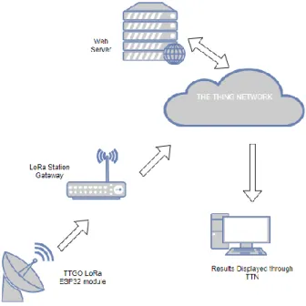
My Network:
A little diagram of our particular case IoT network:
Figure 20 my network
2.2. Lora endpoint realization examples, chipsets and their
comparison.
Popular ESP32 LoRa boards
The following boards are popular for prototyping because they combine an ESP32, a LoRa tranceiver, an OLED 128x64 display:
• Heltec Wifi LoRa 32 • TTGO LoRa32
27
This boards are supposed to bring a Li-ion battery, but in my case it doesn´t.
LoRa antenna: external, connected via cable with I-PEX connector; 868MHz have 5cm external whip antenna with SMA connector; 433MHz have a helical wire antenna.
WiFi/Bluetooth antenna: single on-board.
There is a dedicated LED (non-programmable) for the battery. It is on when the battery is charged. When no battery is connected: it is off when powered via 3.3V pin but flashes
when powered via USB or 5V pin.
A second LED (white on Heltec, blue on TTGO) (programmable) is connected to pin 25, on TTGO V2 the LED is connected to pin 22 but it is useless (see below).
LoRa Performance
The LoRa performance of the Heltec and TTGO boards has shown to be sub-optimal. Important factors are the quality of the RF circuitry (design) and the antennas. Because of the hardware, the range of communications for those circuits is so short, for example for the TTGO the range is no much more than 600 meters.
-Heltec Wifi LoRa 32 [10]
Have a white PCB and come in two different versions (the version numbers are not used by Heltec):
V1: with on-board PCB WiFi/Bluetooth antenna. Appears to be available for 433MHz only.
V2: with small on-board helical antenna (has a PCB antenna on the bottom but that is not connected).
-TTGO LoRa32 [11]
28
• LoRa (without 32): with on-board PCB Wifi/Bluetooth antenna on top. Appears to be available for 433MHz only. Also available without the display.
• LoRa32 V1: with on-board metal Wifi/Bluetooth antenna on bottom. I-Pex connector located on top, it has a SX1276 LoRa transceiver module, and a OLED display controlled by a SSD1306. This will be our particular selection.
• LoRa32 V2: with on-board metal Wifi/Bluetooth antenna on bottom (in a
different location).
Uses ESP32-Pico-D4 (with integrated flash memory) instead of ESP32, uses a (shielded) LoRa module, I-Pex connector located on the bottom, micro-USB connector is rotated 90 degrees, in addition has a micro-SD card slot on the bottom and an on/off switch for the battery next to the micro-USB connector. Switches the battery only so not possible to switch the board off when connected to USB for charging the battery.
‘Programmable’ LED on pin 22 instead of pin 25 but useless because wired to SCL and all three LEDs are on the bottom side where you cannot see them. DIO1 and DIO2 each have a separate board pin but neither of them is connected to a GPIO port so must be explicitly wired. This also means that the TTGO V2 has two GPIO ports less that could otherwise have been used for other purposes.
2.3. Environmental sensors and their data acquisition.
2.3.1. Humidity and temperature sensor
Based on a unique capacitive cell, these relative humidity sensors [12] are designed for high volume, cost sensitive applications such as office automation, automotive cabin air control, home appliances, and industrial process control systems. They are also useful in all applications where humidity compensation is needed.
29
Figure 21 DHT11 with his pinout and how to connect it with a controller [12]
Table 1 Characteristics of the DHT11, (Ta=25º and the measurement frequency is 10KHz) [13]
2.3.2. HL 69 Soil hygrometer moisture sensor
30
The digital output can be connected directly to an Arduino to detect high and low by the microcontroller to detect soil moisture. A typical example of use is when we directly drive the digital outputs to the buzzer module, which can be used as a soil moisture alarm equipment. Analog output AO connected through the AD converter, you can get more precise values of soil moisture sent to your MCU.
Characteristics:
Operating voltage: 3.3V~5V
– Dual output mode – Digital or Analog – analog output more accurate – Fixed bolt hole for easy installation
– Power indicator (red) and digital switching output indicator (green) – LM393 comparator chip, stable
– Panel PCB Dimension: Approx.3cm x 1.5cm – Soil Probe Dimension: Approx. 6cm x 3cm – Cable Length: Approx.21cm
Interface Description(4-wire):
VCC: 3.3V-5V GND: GND
DO: digital output interface (0 and 1) AO: analog output interface
31
Figure 23 Arduino example of how to connect the two parts of this sensor to read data [13]
2.3.3. Ultrasonic distance sensor HC-SR04
Figure 24 pinout of the HC-SR04 [14]
The HC-SR04 [14] sensor its ultrasonic distance sensor able to detect objects and calculate the distance of them to it, but this distances has to be on a range between 2 and 450 cm for the sensor to work properly.
This sensor works using ultrasonic waves and has all the electronic responsible of making the measurement and providing a trigger signal. Its way of use it´s simple, the device send a starting pulse and then measuring the length of the return pulse.
Each HC-SR04 module includes an ultrasonic transmitter, a receiver and a control circuit.
It sends one pulse through the transmitter and this pulse reflects and come back to the sensor
through the receiver we receive that information.
32 Characteristics
• Circuit dimensions: 43 x 20 x 17 mm • Tensión de alimentación: 5 Vcc • Working Current 15mA
• Measuring Angle 15 degree • Frecuencia de trabajo: 40 KHz • Maximum range: 4.5 m
• Minimum range: 1.7 cm
• Minimum trigger pulse duration (TTL level Time-to-live): 10 μS. • Eco output pulse duration(TTL level Time-to-live): 100-25000 μS.
• Minimum waiting time between one measure and the start of the next one: 20 mS.
Pinout:
• VCC
• Trig (Ultrasoud launch) • Echo (ultrasound reception) • GND
We could easily calculate the distance to the target with this simple ecuation:
33
Figure 25 example of how to read data from the HC-SR04 with an Arduino UNO [14]
From a more technical perspective the pulse transmission will be more explained in detail: You
only need to supply a short 10uS pulse to the trigger input to start the ranging, and then the module
will send out an 8 cycle burst of ultrasound at 40 kHz and raise its echo.
34
2.3.4. Sensor de temperature LM35
This is going to be our selection, so we will talk about it later.
2.3.5. MMA7361 Accelerometer sensor
Figure 27 MMA736 accelerometer sensor [15]
This sensor is an analog accelerometer of 3 exes (x,y,z) [15]. The level of the measurements of
the accelerometer allows us to measure the acceleration or the inclination of a platform or surface
of a object in regards to the earth´s surface.
Another features of this sensor are: the sleep mode, the signal conditioning, low pass filter of 1
pole, temperature compensation, auto-test and 0 g detection for free fall. This sensor works with
power sources between 2.2 V and 3.6 VDC (3.3 V is the optimal value).
Sensor specifications MMA7361:
• Low power current: 400 μA.
• Waiting mode: 3 μA.
• Low operating voltage: 2,2 V – 3,6 V.
• High sensibility (800 mV / g@1.5g).
• Selectable sensibility (± 1,5 g, ± 6 g).
• 0g- Detect for the free fall protection.
35 Sensor pinout:
Figure 28 MMA736 pinout [15]
Pinout of the MMA736
• X exe: It is an analog output signal along the X axis.
• Y exe: It is an analog output signal along the Y axis.
• Z exe: It is an analog output signal along the Z axis.
• Sleep(SL): This pin is activated in a negated way the integrated one will go to sleep and
will not send us anything in its outputs. operation will resume when more power is
consumed.
• Detect (0G): This pin will be high when 0 g is detected on all 3 axes. Useful for detecting
free fall
• 5 V: This pin is connected to a built in regulator that will bring 5v to 3.3v required on the
chip to run
• 3.3 V: This pin does not pass through the 5v regulator, it is for those who have a
previously regulated 3.3v voltage.
• Ground (GND): This pin must be connected to circuit ground.
• Sense select (GS): This pin is an enabling pin for the x, y, and z sensors. This must be
enabled at low level, and then the power and ground pins are subtracted. is used to select
between the two sensitivities. If this pin is low, it is in 1.5 g mode. If it is high, it switches
to 6 g mode.
• Self Test (ST): This chip has been built in a self-test to verify that both the mechanical
36
37
3.DESIGN PART.
3.1. Sensor selection and requirements for data reading.
The LM35 it’s an analog temperature sensor and differs with the classic thermistors in the way of
measure the degrees, the classical thermistors measure it changing its electric resistance. The
LM35 it’s an integrated with its own control circuit, which provides an analog output voltage in
proportion to the temperature.
The output of the LM35 is lineal with the temperature, increasing it 10 mV for each degree
centigrade. The acceptable measure range goes from the -55ºC (-550mV) to the 150ºC (150mV).
Its accuracy at ambient temperature is 0.5ºC (25ºC). [16]
Figure 30 Pinout of the LM35 [16]
Figure 31 Bottom view of LM35 LP package [16]
38 Technical features:
• Linear + 10-mV/°C Scale Factor
• 0.5°C Ensured Accuracy (at 25°C)
• Rated for Full −55°C to 150°C Range
• Suitable for Remote Applications
• Low-Cost Due to Wafer-Level Trimming
• Operates From 4 V to 30 V
• Less Than 60-μA Current Drain
• Low Self-Heating, 0.08°C in Still Air
• Non-Linearity Only ±¼°C Typical
• Low-Impedance Output, 0.1 Ω for 1-mA Load
• Calibrated directly in Celsius (Centigrade)
Maximum supported electrical ratings:
Table 2 Maximum electrical ratings for the LM35 [16]
It’s also recommended for this sensor to work between -55ºC and 150ºC.
Application form:
39
Figure 32 basic temperature sensor (2ºC to 150ºC) [16]
Figure 33 full range centigrade temperature sensor [16]
We have selected the first type of implementation, because we don´t need a great range of measurements for this project, we can manage with the easy one, moreover at this time of the year there is no possibility to record values below 2º. So our range of sensing will be between 2ºC and 100ºC more or less, it will be powered with 5 V while the ADC of the ESP 32 can just read between 0 V and 3.3 V, but as we have said, with the values that we are going to work it won´t be a problem, we won´t break the board.
Possible error on the measure:
40
Figure 34 Accuracy vs Temperature (Ensured) [16]
Power supply advice:
This sensor has wide range of valid values (4V to 30V), so it’s an easy to use-and-success IC for many applications. But for noisy environments is recommended to add a 0.1 uF capacitor from the V+ to the GND to bypass the supply voltage and make it more stable, reducing the total amount of noise.
Linearity of the ESP32 ADC measures with the LM35:
Figure 35 sensor volt input versus the ESP32 adc output. [17]
41
3.2. Functional diagram design.
Figure 36 Simple Connections Diagram
42
3.3. Microcontroller selection. Parameters, connectivity and
toolset of ESP32.
3.3.1. Introduction
Created by Espressif Systems, ESP32 is a low-cost, low-power system on a chip (SoC) series with Wi-Fi & dual-mode Bluetooth capabilities.
At its heart, there's a dual-core or single-core Tensilica Xtensa LX6 microprocessor with a clock rate of up to 240 MHz. ESP32 is highly integrated with built-in antenna switches, RF balun, power amplifier, low-noise receive amplifier, filters, and power management modules. Engineered for mobile devices, wearable electronics, and IoT applications, ESP32 achieves ultra-low power consumption through power saving features including fine resolution clock gating, multiple power modes, and dynamic power scaling. [18]
3.3.2. Parameters of ESP32
• Processors:
o Main processor: Tensilica Xtensa 32-bit LX6 microprocessor
▪ Cores: 2 or 1 (depending on variation) All chips in the ESP32 series are dual-core except for ESP32-S0WD, which is single-core. ▪ Clock frequency: up to 240 MHz
▪ Performance: up to 600 DMIPS
o Ultra-low power co-processor: allows you to ADC conversions, computation, and level thresholds while in deep sleep.
• Wireless connectivity:
o Wi-Fi: 802.11 b/g/n/e/i (802.11n @ 2.4 GHz up to 150 Mbit/s) o Bluetooth: v4.2 BR/EDR and Bluetooth Low Energy (BLE) • Memory:
o Internal memory:
43
▪ RTC fast SRAM: 8 KiB For data storage and main CPU during RTC Boot from the deep-sleep mode.
▪ RTC slow SRAM: 8 KiB For co-processor accessing during deep-sleep mode.
▪ eFuse: 1 Kibit Of which 256 bits are used for the system (MAC address and chip configuration) and the remaining 768 bits are reserved for customer applications, including Flash-Encryption and Chip-ID.
▪ Embedded flash: Flash connected internally via IO16, IO17, SD_CMD, SD_CLK, SD_DATA_0 and SD_DATA_1 on ESP32-D2WD and ESP32-PICO-D4.
• 0 MiB (D0WDQ6, D0WD, and ESP32-S0WD chips)
• 2 MiB (ESP32-D2WD chip)
• 4 MiB (ESP32-PICO-D4 SiP module)
o External flash & SRAM: ESP32 supports up to four 16 MiB external QSPI flashes and SRAMs with hardware encryption based on AES to protect developers' programs and data. ESP32 can access the external QSPI flash and SRAM through high-speed caches.
▪ Up to 16 MiB of external flash are memory-mapped onto the CPU code space, supporting 8-bit, 16-bit and 32-bit access. Code execution is supported.
▪ Up to 8 MiB of external flash/SRAM memory are mapped onto the CPU data space, supporting 8-bit, 16-bit and 32-bit access. Data-read is supported on the flash and SRAM. Data-write is supported on the SRAM. ESP32 chips with embedded flash do not support the address mapping between external flash and peripherals. • Peripheral input/output: Rich peripheral interface with DMA that includes
44
• Security:
o IEEE 802.11 standard security features all supported, including WFA, WPA/WPA2 and WAPI
o Secure boot o Flash encryption
o 1024-bit OTP, up to 768-bit for customers
o Cryptographic hardware acceleration: AES, SHA-2, RSA, elliptic curve cryptography (ECC), random number generator (RNG)
Figure 38 ESP 32 block diagram [18]
3.3.3. Toolset
Steps to install Arduino ESP32 support on Windows [19]:
*Tested on 32 and 64 bit Windows 10 machines
1. Download and install the latest Arduino IDE Windows Installer from arduino.cc 2. Download and install Git from git-scm.com
45
o Select Clone Existing Repository
Figure 39 Git Gui menu
o Select source and destination
▪ Sketchbook Directory:
Usually C:/Users/[YOUR_USER_NAME]/Documents/Arduino a nd is listed underneath the "Sketchbook location" in Arduino preferences.
▪ Source Location: https://github.com/espressif/arduino-esp32.git
▪ Target
Directory: [ARDUINO_SKETCHBOOK_DIR]/hardware/espress if/esp32
▪ Click Clone to start cloning the repository
o open a Git Bash session pointing
to [ARDUINO_SKETCHBOOK_DIR]/hardware/espressif/esp32 and execute git submodule update --init --recursive
46
Figure 40: execution of get.exe
o When get.exe finishes, you should see the following files in the directory
Figure 41 new get files
47
5. Start Arduino IDE
6. Select your board in Tools > Board menu
7. Select the COM port that the board is attached to
8. Compile and upload (You might need to hold the boot button while uploading)
ESP 32 Pinout:
Figure 42 ESP 32 pinout [20]
48
Figure 43 TTGO ESP32 LoRa module V1 [19]
3.4. Lora chip selection. Parameters, connectivity and
programming of SX1276.
3.4.1. Introduction
Semtech’s LoRa transceivers feature a long-range wireless modem that provides ultra-long range spread spectrum communication and high interference immunity while minimizing current consumption.
49
3.4.2. Parameters
• integrated +20dBm power amplifier LoRa Modem • 168dB maximum link budget
• +20dBm - 100 mW constant RF output vs. V supply • +14dBm high efficiency Power Amplifier
• Programmable bit rate up to 300kbps • High sensitivity: down to -148dBm • Bullet-proof front end: IIP3 = -11dBm • Excellent blocking immunity
• Low RX current of 9.9mA, 200nA register retention • Fully integrated synthesizer with a resolution of 61Hz • FSK, GFSK, MSK, GMSK, LoRa and OOK modulation • Built-in bit synchronizer for clock recovery
• Preamble detection
• 127dB Dynamic Range RSSI
• Automatic RF Sense and CAD with ultra-fast AFC • Packet engine up to 256 bytes with CRC
• Built-in temperature sensor and low battery indicator
3.4.3. Connectivity
To connect LoRa module with the ESP32 microprocessor we are using the SPI protocol with Arduino, so a brief introduction to his protocol will be needed:
50
• MISO (Master In Slave Out) - The Slave line for sending data to the master, • MOSI (Master Out Slave In) - The Master line for sending data to the peripherals, • SCK (Serial Clock) - The clock pulses which synchronize data transmission generated by
the master
And one line specific for every device:
• SS (Slave Select) - the pin on each device that the master can use to enable and disable specific devices.
When a device's Slave Select pin is low, it communicates with the master. When it's high, it ignores the master. This allows you to have multiple SPI devices sharing the same MISO, MOSI, and CLK lines
Here it is show and example of the SPI protocol working with a time diagram. This interface gives access to a configuration register to select and configure how are is the IC going to access the register, we have: single, burst and FIFO. They difference each other in the way that the frame is composed, in the first one after the address byte, there is only one data byte, in the second there are a bunch of them like in the third, so on the last two you don´t need the address byte to be sent each time, it´s enough with the first address byte, then the BURST method increment its address value and the FIFO the address is memorized [21].
SINGLE access: an address byte followed by a data byte is sent for a write access whereas an address byte is sent, and a read byte is received for the read access.
The NSS pin goes low at the beginning of the frame and goes high after the data byte.
51
MOSI is generated by the master on the falling edge of SCK and is sampled by the slave (i.e. this SPI interface) on the rising edge of SCK. MISO is generated by the slave on the falling edge of SCK. A transfer is always started by the NSS pin going low. MISO is high impedance when NSS is high.
The first byte is the address byte. It is comprising:
• A wnr bit, which is 1 for write access and 0 for read access.
• Then 7 bits of address, MSB first. The second byte is a data byte, either sent on MOSI by the master in case of a write access or received by the master on MISO in case of read access. The data byte is transmitted MSB first.
Proceeding bytes may be sent on MOSI (for write access) or received on MISO (for read access) without a rising NSS edge and re-sending the address. In FIFO mode, if the address was the FIFO address then the bytes will be written / read at the FIFO address. In Burst mode, if the address was not the FIFO address, then it is automatically incremented for each new byte received. The frame ends when NSS goes high. The next frame must start with an address byte. The SINGLE access mode is therefore a special case of FIFO / BURST mode with only 1 data byte transferred. During the write access, the byte transferred from the slave to the master on the MISO line is the value of the written register before the write operation [22].
52
Definition name in Arduino
Pin mapping Type of the pin in
TTGO Lora
Module
SCK Pin 5 GPIO 5 LoRa_SCK
MISO Pin 19 GPIO 19 LoRa_MOSI
MOSI Pin 27 GPIO 27 LoRa_MOSI
SS Pin 18 GPIO 18 LoRa_CS
RST Pin 14 GPIO 14 LoRa_RST
DIO Pin 26 GPIO 26 LoRa_IRQ
Table 3 pin connection SX1276 with ESP32
3.4.4. Programming
The first thing we need to start writing code to control the SX1276 transceiver is to include a couple of useful and must-install Arduino libraries:
The first one the Lora.h library, for sending and receiving data using LoRa radios, supports Semtech SX1276 base boards and shields.
The SPI.h library, this library allows you to communicate with SPI devices, with the Arduino as the master device.
53
3.5. OLED display with SSD1306 controller connection and
programming.
3.5.1. Introduction
An OLED display its similar to a LED/LCD display, in which the light is provided by a external source, besides the OLED display use organic LEDs that has autonomous lightning, this feature makes the OLED displays even thinner, and probably the thinnest technology.
The brain that will tell our display what to do is going to be the SSD1306 controller. It’s a single-chip CMOS OLED/PLED driver with controller for organic/polymer light emitting diode dot-matrix graphic system. It consists of 128 segments and 64 commons. This integrated circuit is designed for Common Cathode type OLED panel.
54
3.5.2. Connection
Figure 46 SSD1306 controller and OLED display
In this picture we can see how the interface between the OLED display and his controller will take place through the common and the segment pins, which will tell which pixels have to turn up.
55
In the following picture we can see the exact connections that we are supposed to do if we want to connect the SSD1306 controller with any other MCU that provides him the data to display, there also a couple of capacitors that are recommend to use, and last but not least the power source with a couple of parallel capacitors to maintain the value constant.
Figure 48 SSD1306 controller connections needed to work with any other device
56
Figure 49 Block diagram of the SSD1306 OLED dislpay controller [23]
Segments driver / Common driver:
57
Figure 50 Communication diagram between a MCU the Seg/Com driver and the OLED display
Graphic display Data RAM (GDDRAM):
This is a bit mapped static RAM that has the pattern about to be displayed, this RAM has 128 x 64 bits and divided that ones into pages, from 0 to 7. Each page it’s like a row of a matrix, containing all the segments from 0 to 127, and a group of commons, actually 8 commons each page.
58
Figure 52 Detailed pages of the SSD1306 [23]
The controller gives us the possibility to select the interface protocol that we will use to “talk” with it. This is possible because of a group of three-bit pins: BS0, BS1, BS2 that taking HIGH or Low different combinations of values will select the protocol. For example in our case, I2C communication ks selected with the combination: [ BS0, BS1 , BS2 ] = [ 0 , 1 , 0 ]
Table 4 MCU bus interface pin selection [23]
Note:
(1) 0 is connected to VSS (2) 1 is connected to VDD
Table 5 MCU interface assignment under different bus interface mode [23]
59
for the SCL (we will explain these concepts later); mine while the other digital pins (from D7 to D3) will remain at a low level. In addition, we will need a couple of control signals: in the pin D/C# it will take place the SA0, and in the RES# pin we will have the RES# (regular reset); and the E, R/W# and CS# will remain LOW.
Figure 53 pinout scheme of the SSD1306 controller [23]
I2C interface protocol:
To connect OLED Display with the ESP32 microprocessor we are using the I2C protocol with Arduino, so a brief introduction to his protocol will be needed:
60
Like UART communication, I2C only uses two wires to transmit pure data and commands between two devices: SDA and SCL, but it also needs two more wires for control: SA0: slave address bit, to recognise the slave address before the transmission, but as we had said earlier we are connection just two things, so we won´t need this wire. This one is needed when we have a bunch of slaves or masters.
RST or RES#: is used for the initialization of device before start transmitting its need to restart de device and his parameters.
Figure 54 Master-Slave communication with I2C interface basic diagram [24]
SDA (Serial Data) – The I2C bus data signal, communication channel between master and slave, not just data, also ACK is sent through that.
61
Figure 55 ACK message example [23]
SCL (Serial Clock) – The line that carries the clock signal. Each transmission of data bit takes place during a single clock period of SCL.
Figure 56 example of the SCL functioning [23]
Like SPI, I2C is synchronous, so the output of bits is synchronized to the sampling of bits by a clock signal shared between the master and the slave. The clock signal is always controlled by the master.
62
Figure 57 I2C bus data format in the write mode [23]
As we are going to use a I2C protocol to communicate the OLED Display and the ESP32 microprocessor, the pin mapping will be according to the OLED_LoRa_sender.ino code (first board test), (Remember we are using V1):
Definition name in arduino
Pin mapping Type of the pin in TTGO Lora Module
OLED_SCL Pin 15 GPIO 5
OLED_SDA Pin 4 GPIO 19
OLED_RST Pin 16 GPIO 16
Table 6 pin connection of SSD1306 with ESP32
3.5.3. Programming
The first thing we need to start writing code to control the SSD1306 is to include his own library:
63
This is one of the internal sub-libraries of the OLED library; this library includes a lot of different functions to draw circles, lines, squares, to write words and so on.
To start working with this lib, first we have to initialize our OLED display for the connection with esp32. This is possible with:
SSD1306Wire (uint8_t _address, uint8_t _sda, uint8_t _scl);
This is how the function is initialized with his parameters in the library. To call and use it in our script:
Address = 0x3c
OLED_SDA = 4
OLED_SCL = 15
SSD1306 display (0x3c, 4, 15);
64
3.6. The schematic diagram design (including internal
connections of presented TTGO Lora module).
65
3.7. The data reading and transmission flowchart design.
66
67
Figure 61 Data Transmission Flowchart of the LoRa WAN project
3.8. The program design using Arduino shield with libraries.
3.8.1. OLED_LoRa_sender.ino
Libraries and definitions:
1-SPI.h:
It’s an Arduino proper library, that includes all the commands to perform a proper SPI devices transmission.
Function examples:
68 2-LoRa.h:
This Arduino library is design for communications and transmission between two devices using LoRa technology, just sending and receiving unformatted bits between them. Not even the payload format in a LoRa WAN is used here. This library provides us an interface between our MCU and the LoRa transceiver to then transmit our data with its functions LoRa.beginPacket(), LoRa.print(), LoRa.endPacket().
Functions examples:
LoRa.setPins(SS,RST,DI0); It’s easy to realise that this function will set the I2C communication pins between our transceiver and our MCU, and initialize it.
3-Wire.h:
This library allows you to communicate with I2C / TWI devices. In our particular case we will need to manage the transmissions between the SSD1306 controller and the ESP32 MCU. We won´t use wire methods on this script, it will be used by the other library, the one that mange the OLED display, the SSD1306, but this library has been explained in previous points.
#include <SPI.h>
#include <LoRa.h>
#include <Wire.h>
#include "SSD1306.h"
#include "images.h"
Define all the pin connections that are needed to be made, for the SPI communication between SX1276 and ESP32.
#define SCK 5 // GPIO5 -- SX1278's SCK
#define MISO 19 // GPIO19 -- SX1278's MISO
#define MOSI 27 // GPIO27 -- SX1278's MOSI
69
#define RST 14 // GPIO14 -- SX1278's RESET
#define DI0 26 // GPIO26 -- SX1278's IRQ(Interrupt Request)
#define BAND 868E6
Initializations and declarations:
unsigned int counter = 0; A simple counter that will be increasing
its value to see how the other lora ttgo module receive it and display it correctly.
V1 modification in the ssd1306 controller pin connections for the I2C communication
SSD1306 display(0x3c, 4, 15);
String rssi = "RSSI --";
String packSize = "--";
String packet ;
Void_setup():
void setup() {
pinMode(16,OUTPUT);
pinMode(2,OUTPUT);
digitalWrite(16, LOW); // set GPIO16 low to reset OLED
70
digitalWrite(16, HIGH); // while OLED is running, must set
GPIO16 in high
Serial.begin(9600);
while (!Serial);
Serial.println();
Serial.println("LoRa Sender Test");
SPI.begin(SCK,MISO,MOSI,SS);The function to setup and initialize the SPI communications
LoRa.setPins(SS,RST,DI0);The function to setup and initialize the LoRa
communications
if (!LoRa.begin(868E6)) {To start LoRa technology is so important to put the
European frequency band
Serial.println("Starting LoRa failed!");
while (1);
}
//LoRa.onReceive(cbk); these two lines are commented because are for the
receiver version
//LoRa.receive();
Serial.println("init ok");
display.init(); Initialization of the oled display to start running
display.flipScreenVertically();
display.setFont(ArialMT_Plain_10);
71
delay(1500);
}
Void loop():
void loop() {
display.clear();
display.setTextAlignment(TEXT_ALIGN_LEFT);
display.setFont(ArialMT_Plain_10);
display.drawString(0, 0, "Sending packet: ");
display.drawString(90, 0, String(counter));
display.display();
// send packet, This four commands form the sending “protocol” , just in a metaphorical way
LoRa.beginPacket();This one set the start of the package to send
LoRa.print("hello ");This case we are sending a simple hello + counter number LoRa.print(counter);
LoRa.endPacket();This one set the start of the package to send
counter++;
digitalWrite(2, HIGH); // turn the LED on (HIGH is the voltage level)
delay(1000); // wait for a second
digitalWrite(2, LOW); // turn the LED off by making the voltage LOW
delay(1000);a // wait for a second
72
3.8.2. Ttgo_abp_lorawan.ino
Lmic.h lib explanation:
The LMiC library [25] gives us an event-based programming model where all protocol events are dispatched to the application’s onEvent() call back function the one that takes care of the each instant running event. The timings or interrupts are carried by the built-in libraries that handles the run-time environment, taking care pf timer queues and job management.
The code is run in jobs which are executed on the main thread by the main scheduler function os_runloop(). These so-called jobs are coded as regular C functions and will be managed by the run time functions, the ones that control the run-time environment with his initialization, scheduling and execution of the run-time jobs. For the job management an additional per job control struct osjob_t is required which identifies the job and stores all the information needed to manage and handle it. The jobs should only update state and schedule actions, which will trigger new job or event call-backs.
All an application has to do is to initialize the run-time environment using the os_init() function and to run the job scheduler function os_runloop(), which does not return. In order to launch all the protocol actions and generate events, an initial job needs to be set up. Therefore, a start-up job is scheduled using the os_setCallback() function, in our particular case we are using the os_setTimedCallback() function, which differs with the other in the time when job is going to be prepared to run. The first job prepares a immediately runnable job and the second one scheduled a timed job fixed with the absolute system time.
Hal/hal.h lib explanation:
73
Figure 62 Diagram of the place that Hardware abstraction layer takes up in the LMIC library and that on the LoRa WAN architecture [25]
To understand how this library works we are going to review a couple of examples of the Hal library functions:
void hal_init (): Initialize the hardware abstraction layer and configure the
components for: IO, SPI, TIMER, IRQ for other hal functions.
void hal_failed (): Perform a fatal failure situation resetting everything to a
safe state position.
void hal_pin_rxtx (u1_t val): Drive the digital output pins RX and TX
(0=receive, 1=transmit) getting them prepared to transmit.
U8x8lib.h lib explanation:
This lib it’s so similar to the SSD1306 library we use previously on the lora sender and receiver example, we use this now because it’s the one that had been tested for the LoRa WAN protocol. It has typical display controllers functions like:
u8x8.setCursor(0, 5);
The set cursor function just put the location where we are going to start displaying things.
74
The printf function works exactly equal to the c++ function, it simply displays some characters or numbers.
u8x8.drawString(0, 7, "EV_SCAN_TIMEOUT");
The drawstring function is so similar to printf plus set cursor, because it select the starting position to display and the string to display.
Arduino code:
#include <lmic.h>
#include <hal/hal.h>
#include <SPI.h>
#include <U8x8lib.h>
#define BUILTIN_LED 25
// the OLED used
U8X8_SSD1306_128X64_NONAME_SW_I2C u8x8(/* clock=*/ 15, /*
data=*/ 4, /* reset=*/ 16); The OLED controller pin connections for the
I2C communication with the ESP32.
// LoRaWAN NwkSKey, network session key
This is the default Semtech key, which is used by the early prototype TTN network.
static const PROGMEM u1_t NWKSKEY[16] = { 0x75, 0x15, 0x56,
0x54, 0x94, 0xD7, 0xCD, 0x35, 0x26, 0x04, 0x61, 0x7A, 0xC9,
0xB5, 0xFC, 0x92 };
// LoRaWAN AppSKey, application session key
This is the default Semtech key, which is used by the early prototype TTN network.
static const u1_t PROGMEM APPSKEY[16] = { 0xAA, 0x3F, 0xAA,
0xFD, 0xCE, 0x05, 0x77, 0xAA, 0xF0, 0x7C, 0x2A, 0x66, 0xCC,
0x6B, 0x7E, 0xAD };
75
static const u4_t DEVADDR = 0x26011467; This address has to be
changed for every node!
These callbacks are only used in over-the-air activation, so they are left empty here (we cannot leave them out completely unless DISABLE_JOIN is set in config.h, otherwise the linker will complain).
void os_getArtEui (u1_t* buf) { }
void os_getDevEui (u1_t* buf) { }
void os_getDevKey (u1_t* buf) { }
static uint8_t mydata[] = "Hello, world!";This is going to be the data that we are going to send
static osjob_t sendjob; the osjob_t is a structure that identifies the job and
stores context information, our job will be called sendjob.
Schedule TX every “n” seconds (might become longer due to duty cycle limitations).
const unsigned TX_INTERVAL = 30;
Pin mapping, to communicate the SX1276 with the ESP32 through the SPI protocol.
const lmic_pinmap lmic_pins = {
.nss = 18, This is the salve selection pin
.rxtx = LMIC_UNUSED_PIN,
.rst = 14, This is the reset pin, RST.
.dio = {26, 33, 32}, This are going to be the MISO, MOSI and
IRQ pins.
};
void onEvent (ev_t ev):
76
void onEvent (ev_t ev) {
Serial.print(os_getTime());
u8x8.setCursor(0, 5);
u8x8.printf("TIME %lu", os_getTime());
Serial.print(": ");
switch(ev) {
case EV_SCAN_TIMEOUT:
Serial.println(F("EV_SCAN_TIMEOUT"));
u8x8.drawString(0, 7, "EV_SCAN_TIMEOUT");
break;
case EV_BEACON_FOUND:
Serial.println(F("EV_BEACON_FOUND"));
u8x8.drawString(0, 7, "EV_BEACON_FOUND");
break;
case EV_BEACON_MISSED:
Serial.println(F("EV_BEACON_MISSED"));
u8x8.drawString(0, 7, "EV_BEACON_MISSED");
break;
case EV_BEACON_TRACKED:
Serial.println(F("EV_BEACON_TRACKED"));
u8x8.drawString(0, 7, "EV_BEACON_TRACKED");
break;
case EV_JOINING:
Serial.println(F("EV_JOINING"));
u8x8.drawString(0, 7, "EV_JOINING");
break;
case EV_JOINED:
Serial.println(F("EV_JOINED"));
u8x8.drawString(0, 7, "EV_JOINED ");
Disable link check validation (automatically enabled during join,
but not supported by TTN at this time).
LMIC_setLinkCheckMode(0); Enable/disable link check
77
break;
case EV_RFU1:
Serial.println(F("EV_RFU1"));
u8x8.drawString(0, 7, "EV_RFUI");
break;
case EV_JOIN_FAILED:
Serial.println(F("EV_JOIN_FAILED"));
u8x8.drawString(0, 7, "EV_JOIN_FAILED");
break;
case EV_REJOIN_FAILED:
Serial.println(F("EV_REJOIN_FAILED"));
u8x8.drawString(0, 7, "EV_REJOIN_FAILED");
break;
case EV_TXCOMPLETE:
The data prepared via LMIC_setTxData2() has been sent, and eventually
downstream data has been received in return. If confirmation was requested, the acknowledgement has been received.
Serial.println(F("EV_TXCOMPLETE (includes waiting
for RX windows)"));
u8x8.drawString(0, 7, "EV_TXCOMPLETE");
digitalWrite(BUILTIN_LED, LOW);
if (LMIC.txrxFlags & TXRX_ACK) If we have flags and
confirmed UP frame was acked
Serial.println(F("Received ack"));
u8x8.drawString(0, 7, "Received ACK");
if (LMIC.dataLen) {
Serial.println(F("Received "));
u8x8.drawString(0, 6, "RX ");
Serial.println(LMIC.dataLen); LMIC.dataLen is one of
the flag binary comands nad part of the LIMIC structure, // 0 no data or zero length data, >0-byte count of data
u8x8.setCursor(4, 6);
u8x8.printf("%i bytes", LMIC.dataLen);
78
u8x8.setCursor(0, 7);
u8x8.printf("RSSI %d SNR %.1d", LMIC.rssi,
LMIC.snr); Received Signal Strength Indicator, the RSSI intensity of the
signal and the SNR signal-to-noise ratio the relation between the signal and the noise.
}
Schedule next transmission
os_setTimedCallback(&sendjob,
os_getTime()+sec2osticks(TX_INTERVAL), do_send);
break;
case EV_LOST_TSYNC:
Serial.println(F("EV_LOST_TSYNC"));
u8x8.drawString(0, 7, "EV_LOST_TSYNC");
break;
case EV_RESET:
Serial.println(F("EV_RESET"));
u8x8.drawString(0, 7, "EV_RESET"); break;
case EV_RXCOMPLETE:
// data received in ping slot
Serial.println(F("EV_RXCOMPLETE"));
u8x8.drawString(0, 7, "EV_RXCOMPLETE");
break;
case EV_LINK_DEAD:
Serial.println(F("EV_LINK_DEAD"));
u8x8.drawString(0, 7, "EV_LINK_DEAD");
break;
case EV_LINK_ALIVE:
Serial.println(F("EV_LINK_ALIVE"));
u8x8.drawString(0, 7, "EV_LINK_ALIVE");
break;
default:
Serial.println(F("Unknown event"));
u8x8.setCursor(0, 7);
![Figure 1 LoRa WAN architecture and devices classes [7]](https://thumb-us.123doks.com/thumbv2/123dok_es/6133963.179864/14.892.199.703.418.663/figure-lora-wan-architecture-devices-classes.webp)
![Figure 3 Up-Chirp spread spectrum modulation example in time domain [6]](https://thumb-us.123doks.com/thumbv2/123dok_es/6133963.179864/16.892.266.638.255.494/figure-chirp-spread-spectrum-modulation-example-time-domain.webp)
![Figure 11 Class B type device transmission [8]](https://thumb-us.123doks.com/thumbv2/123dok_es/6133963.179864/22.892.128.827.202.890/figure-class-b-type-device-transmission.webp)
![Figure 14 Class C device timing diagram [8]](https://thumb-us.123doks.com/thumbv2/123dok_es/6133963.179864/23.892.177.766.289.828/figure-class-c-device-timing-diagram.webp)
![Table 1 Characteristics of the DHT11, (Ta=25º and the measurement frequency is 10KHz) [13]](https://thumb-us.123doks.com/thumbv2/123dok_es/6133963.179864/29.892.272.618.131.526/table-characteristics-dht-ta-º-measurement-frequency-khz.webp)
![Figure 22 pinout of the controller of the HL69 [13]](https://thumb-us.123doks.com/thumbv2/123dok_es/6133963.179864/30.892.214.682.796.1037/figure-pinout-controller-hl.webp)
![Figure 26 HC-SR04 trigger and echo transmission timing diagram [14]](https://thumb-us.123doks.com/thumbv2/123dok_es/6133963.179864/33.892.184.709.200.534/figure-hc-sr-trigger-echo-transmission-timing-diagram.webp)
![Figure 35 sensor volt input versus the ESP32 adc output. [17] Resolution 3.3V/4096 = 0.000805664 V = 0.8 mV](https://thumb-us.123doks.com/thumbv2/123dok_es/6133963.179864/40.892.260.623.132.458/figure-sensor-volt-input-versus-esp-output-resolution.webp)

