Atomistic modeling of ion implantation technologies in silicon
Luis A. Marqués
1, Iván Santos, Lourdes Pelaz, Pedro López, María Aboy
Departamento de Electrónica, Universidad de Valladolid, E.T.S.I. de Telecomunicación, 47011 Valladolid, Spain
Abstract
Requirements for the manufacturing of electronic devices at the nanometric scale are becoming more and more demanding on each new technology node, driving the need for the fabrication of ultra-shallow junctions and finFET structures. Main implantation strategies, cluster and cold implants, are aimed to reduce the amount of end-of-range defects through substrate amorphization. During finFET doping the device body gets amorphized, and its regrowth is more problematic than in the case of conventional planar devices. Consequently, there is a renewed interest on the modeling of amorphization and recrystallization in the front-end processing of Si. We present multi-scale simulation schemes to model amorphization and recrystallization in Si from an atomistic perspective. Models are able to correctly predict damage formation, accumulation and regrowth, both in the ballistic and thermal-spike regimes, in very good agreement with conventional molecular dynamics techniques but at a much lower computational cost.
Keywords: Si; B; Implantation; Annealing; Amorphization; Recrystallization; Atomistic simulation; Multi-scale schemes; Molecular dynamics; Binary Collisions; Kinetic Monte Carlo.
1.Introduction
CMOS technology is being pushed closer to its limits. In particular, front-end processing is trying to extend the use of conventional techniques, such as ion implantation and annealing, for the manufacturing of ultra-shallow junctions and finFET devices [1]. At junction level, gate length scaling has driven a progressive reduction of the junction depth at the source and drain extensions in order to keep a good control of short channel effects. Simultaneously, high dopant activation in source and drain regions is required to reduce access resistance and achieve high drive currents. Besides, end-of-range defects density should be kept low in order to reduce off-state leakage currents, which is important in low-power applications. To address these issues, proposed ion implantation strategies, mainly cluster and cold implants, are aimed to minimize residual damage through substrate amorphization. Another issue is related to the regrowth of finFET devices [2]. The fin body gets amorphized during doping and its regrowth is more problematic than in the case of planar devices. Consequently, there is a renewed interest on the modeling of amorphization and recrystallization in the front-end processing of Si.
Unfortunately, traditional models lack of predictive capabilities. They assume that the lattice turns amorphous if a critical point defect concentration is exceeded [3]. Recrystallization occurs instantaneously, and only defects beyond the original amorphous-crystal interface remain. One of the main limitations of this simplistic view is the uncertainty in the critical point defect concentration value: due to the steepness of the damage profile, a little variation in the predicted depth of the amorphous-crystal interface can lead to changes up to 50% in the residual damage concentration. The exact amount of this residual damage is of great relevance as it significantly affects dopant diffusion and activation [4].
For the model to be predictive and accurate, it must encompass the physics involved in the technological processes, and should take into account the atomistic nature of the material, since typical device features are in the nanometer scale. Among the atomistic simulation techniques, fundamental methods such ab initio, tight binding (TB) and molecular dynamics (MD) with empirical potentials, are able to give very detailed information on the
simulated system at the atomic level. However, space and time scales accessible to these techniques are very far from actual processing conditions. To get closer to real processing scales it is necessary to use less detailed methods, where not all the particles in the system are considered, only those involved in events which are relevant to the simulated process are taken into account. Binary collision (BC) models are specifically designed to efficiently simulate the implantation process by assuming that collisions only occur between pairs of atoms [5]. On the other hand, kinetic Monte Carlo (kMC) codes allow the simulation of the annealing step by following only the dynamics of dopants and defects and their interactions [6]. However, in these event-based techniques, a lot of parameters must be specified a priori, such as displacement and binding energies, defect diffusivities, emission probabilities, etc.
Consequently, it is easy to realize that you cannot use just one of these techniques to get full front-end processing simulation. All of them have to be used in a hierarchical or multi-scale scheme [7,8]. Fundamental techniques such as ab-initio and TB can be employed to study defect configurations and energetics, material and electronic properties, and to optimize empirical potentials along with experimental data. MD simulations with empirical potentials in turn can be used to determine interaction and diffusion mechanisms involving defects, or to study the damage morphology obtained from individual implantation cascades as well as its annealing behavior. All these data along with experimental measurements will define the relevant events, models and parameters to be considered in the BC and kMC simulators. The BC code is used to calculate the implantation cascades. The coordinates of dopants and generated defects are fed to the kMC simulator at time intervals determined by the dose-rate. This procedure is repeated until the specified dose is reached. Additional annealing steps can be run with the kMC simulator. Time consuming simulations and measurements are carried off-line, while actual processing simulation is obtained by the BC and kMC loop, much faster methods. If models and parameters are good, it is possible to obtain meaningful results in a reduced amount of computation time.
Based on this kind of multi-scale schemes, we have developed: (a) an atomistic model for amorphization and recrystallyzation in Si based on MD simulations, that will be presented in Section 2; and (b) an improved BC model able to correctly describe damage morphology from cluster implantations, that will be presented in Section 3. The combination of these two models allows the fast simulation of the full implantation and annealing cycles in Si at the atomic level, especially for amorphizing conditions which are not correctly predicted in conventional BC models.
2.Atomistic model for Si amorphization and recrystallization
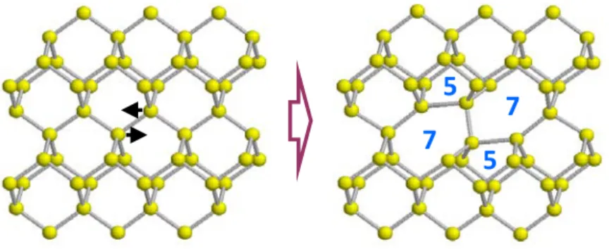
We have constructed an atomistic model for describing Si amorphization and recrystallization based on the so called bond defect. It consists of a local rearrangement of bonds in the crystal with no excess or deficit of atoms (see Fig. 1). It introduces in the Si lattice the five- and seven-membered rings typical of the amorphous phase while maintaining perfect four-fold coordination. Amorphization can be produced by accumulation of bond defects. In fact, when you introduce bond defects in the Si lattice up to a concentration of 25%, the structure that you get is identical to the corresponding to the amorphous phase [9].
7
7
5
5
Fig. 1. Schematics of the bond defect formation.
be generated as a primary defect resulting from collision events, with no need of pre-existing interstitials and vacancies in the lattice for its formation [11].
This defect has been characterized using ab-initio, TB and classical MD techniques [9,10,12,13]. The bond defect formation energy is of the order of the corresponding to typical point defects in Si. However, it has not yet been detected experimentally, maybe because perfect four-fold coordination prevents its detection in standard techniques. The stability of the defect has been also studied, and it has been shown that its lifetime follows an Arrhenius behavior over a wide temperature range with an activation energy of 0.43 eV [9]. At room temperature, the bond defect lifetime is about 3 microseconds, very short in comparison with the characteristic inter-cascade times at typical dose-rates. This indicates that the bond defect itself is not stable enough to accumulate and promote amorphization.
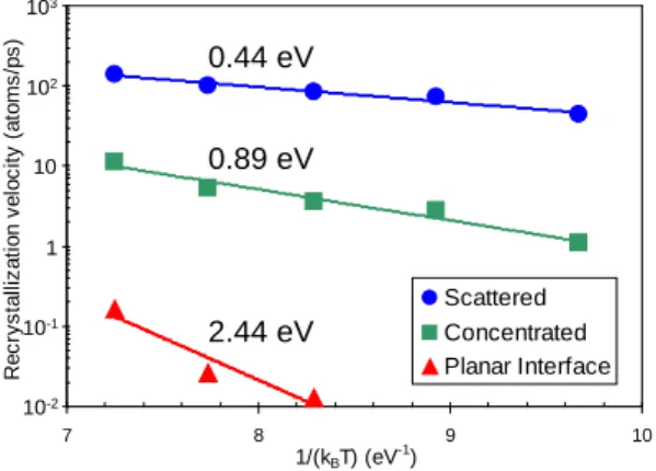
However, the stability of the bond defect increases when other bond defects are close in the lattice. We considered two crystal lattices where we introduced the same amount of bond defects (8%), in one bond defects were distributed randomly, separated each other by a distance of at least 4 Å, and in the other bond defects were arranged in a sphere with a radius of 12 Å. The lattice with scattered bond defects would represent damage generated by light ion implantation, while the system with concentrated bond defects would represent damage generated by heavy ion implantation. Both types of systems were annealed using MD techniques at several temperatures, using the Tersoff 3 potential [14] to describe Si interactions. In all cases the scattered damage disappeared long before the concentrated damage. This indicates that the interaction of bond defects creates more stable damage structures, as it is observed in the experiments, where compact damage is much more stable than dilute damage [15].
Figure 2 shows the recrystallization velocities for both types of systems as a function of temperature. They have Arrhenius behavior. The activation energy for scattered damage regrowth is very close to that corresponding to isolated bond defect recombination, 0.43 eV. This indicates that a 4 Å separation among bond defects was long enough to prevent their interaction. In the case of the concentrated damage the activation energy is higher and recrystallization dynamics slower. Recrystallization starts from the amorphous-crystal interface, as it is also observed in experiments. This is because bond defects in contact with crystalline atoms are less stable than bond defects in the center of the sphere. This effect is enhanced in the case of a planar amorphous-crystal interface. It shows even higher activation energy for recrystallization, 2.44 eV, in very good agreement with the value measured in the experiments, 2.7 eV [16]. In the limit, as already stated, a pure amorphous matrix would be described by bond defects completely surrounded by other bond defects. The recombination of such a bond defect would be equivalent to the generation of a crystal embryo in the amorphous phase. The activation energy for crystal nucleation in amorphous Si has been experimentally determined to be 5 eV [17]. Consequently, the higher the number of surrounding bond defects, the higher the activation energy for bond defect recombination.
7 8 9 10
1/(kBT) (eV-1)
R ec ry s tal li z at ion v el oc it y ( at om s /ps ) Scattered Concentrated Planar Interface 10-2 10-1 1 10 102 103 0.44 eV 0.89 eV 2.44 eV
Fig. 2. Arrenhius plot of the recrystallization velocities obtained in MD annealing simulations of samples with bond defects: (a) scattered, (b) concentrated in a sphere, and (c) arranged in a planar amorphous-crystal interface. Activation energies are shown besides each curve.
collision cascade. Activation energy for bond defect recombination depends on the number of neighboring bond defects: they are more stable as the number of bond defect neighbors increases. Activation energies for recrystallization range from 0.43 eV for isolated bond defects to 5 eV for bond defects completely surrounded by other bond defects. This simple model captures the kinetic features related to amorphization and recrystallization in Si. In fact, it correctly reproduces many experimental observations, for example, the superlinear accumulation of damage with dose [18], the regrowth behavior of individual amorphous pockets [19], and the critical regime between amorphization and recrystallization and its dependence on substrate temperature, dose rate and ion mass [20,21].
3.Improved BC model for cluster ion implantation simulations
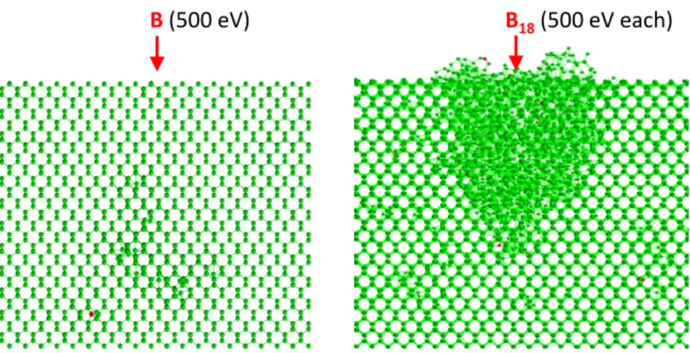
Monatomic B implantation has traditionally been used for the fabrication of shallow junctions. As technology scales down the energies necessary to fabricate junctions, monatomic B implantation shows several shortcomings, mainly related to production-throughput and ion-beam high-energy contamination [22]. The implantation of B clusters has been proposed as an alternative to overcome these drawbacks. Thanks to the development of convenient implantation equipment [22], the fabrication of p-type regions in MOSFET devices using octadecaborane, a
molecule which delivers 18 B atoms, has been successfully demonstrated [23].
When using the same implant energy and dose, dopant profiles obtained from monatomic B or cluster
implantations are almost identical [24]. However, damage profiles are totally different. Figure 3 shows the typical damage produced by a 500 eV B ion, and the corresponding to the impact of an octadecaborane cluster with the same energy per B atom, as predicted by MD (simulation details are given in Ref [24]). On average, a 500 eV B cascade produces only 32 atoms displaced from perfect lattice positions. Damage is dilute and consequently it recombines easily. This explains why it is not possible to amorphize Si with monoatomic B beams at typical dose rates. In the cluster case, the number of displaced atoms per implanted B is more than three times the number obtained in the monatomic case. The simultaneous deposition of the energy carried by the cluster produces a thermal spike that generates a big amorphous region. In this case, damage is compact and consequently much more stable.
B
(500 eV)
B18
(500 eV each)
Fig. 3. Side view of the typical damage generated in a Si substrate after the implantation of a single B ion (left) and an octadecaborane cluster (right), as obtained from MD simulations. Green circles are Si atoms and red circles B atoms.
As it was stated in Section 2, damage regrowth depends on its morphology. MD is able to correctly predict damage morphology produced during the development of implantation cascades, but it is a very computationally expensive simulation technique. In fact, the simulation of an octadecaborane cluster cascade takes 3 hours in a typical parallel computer. Consequently, to simulate the full implantation step to a typical dose of 1015 cm-2
since they are a consequence of low-energy many-body interactions during the thermal spike regime.
In order to overcome this drawback, we developed an improved BC model able to correctly predict the generation of damage by low-energy interactions. First we characterized these interactions by MD simulations with the Tersoff 3 potential. We gave a certain amount of kinetic energy to a number of Si atoms located in a sphere with velocities in random directions. The initial energy of moving Si atoms was varied between 0 and 20 eV per atom, around the displacement threshold for Si [25,26], and the total deposited energy between 50 and 500 eV. At the end of the simulations we counted the number of atoms displaced from perfect lattice positions. We define the efficiency of damage production by this low-energy mechanism as the number of final displaced atoms per initial moving atom.
Figure 4 shows the obtained efficiencies as a function of the initial energy of moving atoms for different total deposited energies. Initial energy density refers to the particular energy value given to every initial moving atom. In BC simulations, moving atoms with energies lower than the displacement threshold will not produce any displacement event, so the efficiency for damage generation is zero. At the displacement threshold a recoil will be generated and consequently the efficiency becomes one. However, in MD the efficiency can be quite high even well below the displacement threshold. This efficiency increases with initial energy of moving atoms and with the total deposited energy. These results indicate that the same amount of deposited energy is more or less efficient in terms of damage generation depending on the energy density.
0 1 2 3 4
0 5 10 15 20
Initial energy density (eV/atom)
E
ff
ic
ie
n
c
y
5 keV 500 eV
300 eV
200 eV
100 eV
50 eV
BC Models
Fig. 4. Efficiencies obtained in MD simulations (see description in the text), as a function of the initial energy of moving atoms for different total deposited energies (values indicated besides each curve). Efficiency predicted by conventional BC models is also shown.
We have used these MD results to incorporate the effect of low energy interactions in BC models. The first step consists of considering all energy transfers to target atoms, and not only those above the displacement threshold. Then these atoms are grouped within a first neighbor distance. Taking into account the number of particles and the total energy of the formed groups, corresponding efficiencies of Fig. 4 are applied to obtain the final amorphous regions, described as additional bond defects.
Bond defects
Fig. 5. Depth projection of damage generated by a 9 keV octadecaborane cascade obtained with the improved BC model. Solid lines are the B ion trajectories. The conventional BC code only provides the position of the interstitials and vacancies generated by the individually implanted B
ions. The improved damage model adds the bond defects representing the amorphous zone, in very good agreement with MD results.
4.Conclusions
To correctly model front-end processing in Si, simulations have to: (a) encompass the physics involved in the technological processes; (b) take into account the atomistic nature of the material; and (c) be organized in multi-scale schemes in order to reach real processing multi-scales. We have applied such multi-multi-scale schemes to develop an atomistic model to describe amorphization and recrystallization processes in Si. The model is able to reproduce many of the experimental observations. Within the framework of this model, we have developed an improved BC algorithm able to provide the same damage morphology as it is obtained from time-consuming MD simulations, for the case of cluster ion implantations where damage is a consequence of low-energy thermal-spike effects. The combination of these two models allows the efficient simulation at the atomic level of the implantation and annealing steps for both amorphizing and sub-amorphizing conditions in Si.
Acknowledgement
This work has been funded by the Spanish Ministerio de Ciencia e Innovación under Project No. TEC2011-27701.
References
1. International Technology Roadmap for Semiconductors, http://www.itrs.net/
2. R. Duffy, M.J.H. Van Dal, B.J. Pawlak, M. Kaiser, R.G.R. Weemaes, B. Degroote, et al., Appl. Phys. Lett. 90 (2007) 241912. 3. S. Prussin, D.I. Margolese and R.N. Tauber, J. Appl. Phys. 57 (1985) 180.
4. P.A. Stolk, H.-J. Gossmann, D.J. Eaglesham, D.C. Jacobson, C.S. Rafferty, G.H. Gilmer, et al., J. Appl. Phys. 81 (1997) 6031. 5. M.T. Robinson, I.M. Torrens, Phys. Rev. B 9, 5008 (1974).
6. M. Jaraiz, P. Castrillo, R. Pinacho and J.E. Rubio, IEDM Technical Digest (2007) p. 951.
10. M. Tang, L. Colombo, J. Zhu and T. Diaz de la Rubia, Phys. Rev. B 55 (1997) 14279. 11. D.M. Stock, B. Weber and K. Gärtner, Phys. Rev. B 61 (2000) 8150.
12. F. Cargnoni, C. Gatti and L. Colombo, Phys. Rev. B 57 (1998) 170. 13. S. Goedecker, T. Deutsch and L. Billard, Phys. Rev. Lett. 88 (2002) 235501. 14. J. Tersoff, Phys. Rev. B 38 (1988) 9902.
15. L. Pelaz, L.A. Marqués, P. López, I. Santos, M Aboy and J. Barbolla, Nucl. Instr. Meth. Phys. Res. B 241 (2005) 501. 16. L. Csepregi, E.F. Kennedy, J.W. Mayer and T.W. Sigmon., J. Appl. Phys. 49 (1978) 3906.
17. Y. Masaki, P.G. LeComber and A.G. Fitzgerald, J. Appl. Phys. 74 (1993) 129. 18. O.W. Holland, S J. Pennycook and G.L. Albert, Appl. Phys. Lett. 55 (1989) 2503.
19. S.E. Donnelly, R.C. Birtcher, V.M. Vishnyakov and G. Carter, Appl. Phys. Lett. 82 (2003) 1860. 20. P.J. Schultz, C. Jagadish, M.C. Ridgway, R.G. Elliman and J.S. Williams, Phys. Rev. B 44 (1991) 9118. 21. R.D. Goldberg, J.S. Williams and R.G. Elliman, Nucl. Instrum. Methods Phys. Res. B 106 (1995) 242. 22. D. Jacobson, T. Horsky, W. Krull and B. Milgate, Nucl. Instrum. Methods Phys. Res. B 237 (2005) 406.
23. Y. Kawasaki, T. Kuroi, T. Yamashita, K. Horita, T. Hayashi, M. Ishibashi et al., Nucl. Instrum. Methods Phys. Res. B 237 (2005) 25. 24. L.A. Marqués, L. Pelaz, I. Santos and V.C. Venezia, Phys. Rev. B 74 (2006) 201201.
25. SRIM documentation, http://www.srim.org/