CNY70
www.vishay.com
Vishay Semiconductors
Rev. 1.8, 30-Jul-12 1 Document Number: 83751
For technical questions, contact: [email protected]
THIS DOCUMENT IS SUBJECT TO CHANGE WITHOUT NOTICE. THE PRODUCTS DESCRIBED HEREIN AND THIS DOCUMENT ARE SUBJECT TO SPECIFIC DISCLAIMERS, SET FORTH AT www.vishay.com/doc?91000
Reflective Optical Sensor with Transistor Output
DESCRIPTION
The CNY70 is a reflective sensor that includes an infrared
emitter and phototransistor in a leaded package which
blocks visible light.
FEATURES
• Package type: leaded
• Detector type: phototransistor
• Dimensions (L x W x H in mm): 7 x 7 x 6
• Peak operating distance: < 0.5 mm
• Operating range within > 20 % relative
collector current: 0 mm to 5 mm
• Typical output current under test: I
C= 1 mA
• Emitter wavelength: 950 nm
• Daylight blocking filter
• Lead (Pb)-free soldering released
• Material categorization: For definitions of compliance
please see
www.vishay.com/doc?99912
APPLICATIONS
• Optoelectronic scanning and switching devices i.e., index
sensing, coded disk scanning etc. (optoelectronic
encoder assemblies).
Notes
(1) CTR: current transfere ratio, I out/Iin
(2) Conditions like in table basic charactristics/sensors
Note
(1) MOQ: minimum order quantity
E D Top view Marking area 19158_1 21835
PRODUCT SUMMARY
PART NUMBER MAXIMUM CTRDISTANCE FOR rel(1)
(mm)
DISTANCE RANGE FOR
RELATIVE Iout > 20 %
(mm)
TYPICAL OUTPUT
CURRENT UNDER TEST (2)
(mA)
DAYLIGHT BLOCKING FILTER
INTEGRATED
CNY70 0 0 to 5 1 Yes
ORDERING INFORMATION
ORDERING CODE PACKAGING VOLUME (1) REMARKS
CNY70 Tube MOQ: 4000 pcs, 80 pcs/tube
-ABSOLUTE MAXIMUM RATINGS
(T
amb= 25 °C, unless otherwise specified)
PARAMETER TEST CONDITION SYMBOL VALUE UNIT
COUPLER
Total power dissipation Tamb≤ 25 °C Ptot 200 mW
Ambient temperature range Tamb - 40 to + 85 °C
Storage temperature range Tstg - 40 to + 100 °C
Soldering temperature Distance to case 2 mm, t £ 5 s Tsd 260 °C
INPUT (EMITTER)
Reverse voltage VR 5 V
Forward current IF 50 mA
Forward surge current tp≤ 10 μs IFSM 3 A
Power dissipation Tamb≤ 25 °C PV 100 mW
CNY70
www.vishay.com
Vishay Semiconductors
Rev. 1.8, 30-Jul-12 2 Document Number: 83751
For technical questions, contact: [email protected]
THIS DOCUMENT IS SUBJECT TO CHANGE WITHOUT NOTICE. THE PRODUCTS DESCRIBED HEREIN AND THIS DOCUMENT ARE SUBJECT TO SPECIFIC DISCLAIMERS, SET FORTH AT www.vishay.com/doc?91000
ABSOLUTE MAXIMUM RATINGS
Fig. 1 - Power Dissipation vs. Ambient Temperature
Notes
(1) Measured with the “Kodak neutral test card”, white side with 90 % diffuse reflectance (2) Measured without reflecting medium
OUTPUT (DETECTOR)
Collector emitter voltage VCEO 32 V
Emitter collector voltage VECO 7 V
Collector current IC 50 mA
Power dissipation Tamb≤ 25 °C PV 100 mW
Junction temperature Tj 100 °C
ABSOLUTE MAXIMUM RATINGS
(T
amb= 25 °C, unless otherwise specified)
PARAMETER TEST CONDITION SYMBOL VALUE UNIT
0 100 200 300
0
95 11071
P - Power Dissipation (mW)
Tamb- Ambient Temperature (°C)
IR - diode Coupled device
Phototransistor
25 50 75 100
BASIC CHARACTERISTICS
(T
amb= 25 °C, unless otherwise specified)
PARAMETER TEST CONDITION SYMBOL MIN. TYP. MAX. UNIT
COUPLER
Collector current VCE = 5 V, IF = 20 mA,
d = 0.3 mm (figure 1) IC
(2) 0.3 1.0 mA
Cross talk current VCE = 5 V, IF = 20 mA, (figure 2) ICX(3) 600 nA
Collector emitter saturation voltage
IF = 20 mA, IC = 0.1 mA,
d = 0.3 mm (figure 1) VCEsat
(2) 0.3 V
INPUT (EMITTER)
Forward voltage IF = 50 mA VF 1.25 1.6 V
Radiant intensity IF = 50 mA, tp = 20 ms Ie 7.5 mW/sr
Peak wavelength IF = 100 mA λP 940 nm
Virtual source diameter Method: 63 % encircled energy d 1.2 mm
OUTPUT (DETECTOR)
Collector emitter voltage IC = 1 mA VCEO 32 V
Emitter collector voltage IE = 100 μA VECO 5 V
CNY70
www.vishay.com
Vishay Semiconductors
Rev. 1.8, 30-Jul-12 3 Document Number: 83751
For technical questions, contact: [email protected]
THIS DOCUMENT IS SUBJECT TO CHANGE WITHOUT NOTICE. THE PRODUCTS DESCRIBED HEREIN AND THIS DOCUMENT ARE SUBJECT TO SPECIFIC DISCLAIMERS, SET FORTH AT www.vishay.com/doc?91000
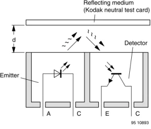
Fig. 2 - Test Condition
BASIC CHARACTERISTICS
(T
amb= 25 °C, unless otherwise specified)
Fig. 3 - Forward Current vs. Forward Voltage
Fig. 4 - Relative Current Transfer Ratio vs. Ambient Temperature
Fig. 5 - Collector Current vs. Forward Current
Fig. 6 - Collector Current vs. Collector Emitter Voltage
~~
~
~ ~
~
A C E C
Detector
Emitter d
95 10893
Reflecting medium (Kodak neutral test card)
0.1 1 10 100 1000 0
VF - Forward Voltage (V)
96 11862
IF
- Forward Current (mA)
1.6 1.2 0.8 0.4 2.0 0.5 0.6 0.7 0.8 0.9 1.0 1.1 1.2 1.3 1.4 1.5 96 11913 CTR
- Relative Current Transfer Ratio
rel
T amb - Ambient Temperature (°C)
- 30
V = 5 V CE
I = 20 mA F
d = 0.3 mm
50 40 30 20 10 0 -10
- 20 60 70 80
0.1 0.001 0.01 0.1 10 I
- Collector Current (mA)
C
I F - Forward Current (mA)
95 11065
1
Kodak neutral card (white side) d = 0.3 mm V CE= 5 V
100 10
1
V CE- Collector Emitter Voltage (V) 95 11066
I F = 50 mA
20 mA 10 mA 5 mA 2 mA 1 mA 0.1 0.001 0.01 0.1 10 I
- Collector Current (mA)
C
1
Kodak neutral card (white side) d = 0.3 mm
100 10
CNY70
www.vishay.com
Vishay Semiconductors
Rev. 1.8, 30-Jul-12 4 Document Number: 83751
For technical questions, contact: [email protected]
THIS DOCUMENT IS SUBJECT TO CHANGE WITHOUT NOTICE. THE PRODUCTS DESCRIBED HEREIN AND THIS DOCUMENT ARE SUBJECT TO SPECIFIC DISCLAIMERS, SET FORTH AT www.vishay.com/doc?91000
Fig. 7 - Current Transfer Ratio vs. Forward Current
Fig. 8 - Current Transfer Ratio vs. Collector Emitter Voltage
Fig. 9 - Collector Current vs. Distance
Fig. 10 - Relative Radiant Intensity/Collector Current vs. Angular Displacement
Fig. 11 - Relative Collector Current vs. Displacement
0.1 1 10 100
0.1
I F - Forward Current (mA) 96 11914
CTR - Current Transfer Ratio (%)
Kodak neutral card (white side) d = 0.3 mm V CE = 5 V
100 10 1 0.1 1 10
V CE - Collector Emitter Voltage (V) 96 12001
C
TR -
C
urrent Transfer Ratio (%)
20 mA 10 mA 5 mA 2 mA
1 mA I F= 50 mA
Kodak neutral card (white side) d = 0.3 mm
0.1 1 10 100
0 0.001 0.1 1 10 I
- Collector Current (mA)
C
d - Distance (mm)
95 11069
V CE = 5 V
I F = 20 mA
d 10 8 6 4 2
I - Relative Radiant Intensityerel
95 11063 0.6 0.9 0.8 0° 30° 10° 20°
40° 50° 60° 70° 80° 0.7 1.0
I - Relative Collector Currentcrel
0.6 0.4 0.2 0 0.2 0.4 0.0 0.1 0.2 0.3 0.4 0.5 0.6 0.7 0.8 0.9 1.0 0
s - Displacement (mm)
96 11915
V CE= 5 V
I F = 20 mA
I - Relative Collector CurrentCrel
d = 5 mm 4 mm 3 mm 2 mm 1 mm 0 E D D E 1.5 d
s 0 5 mm
10 mm
CNY70
www.vishay.com
Vishay Semiconductors
Rev. 1.8, 30-Jul-12 5 Document Number: 83751
For technical questions, contact: [email protected]
THIS DOCUMENT IS SUBJECT TO CHANGE WITHOUT NOTICE. THE PRODUCTS DESCRIBED HEREIN AND THIS DOCUMENT ARE SUBJECT TO SPECIFIC DISCLAIMERS, SET FORTH AT www.vishay.com/doc?91000
PACKAGE DIMENSIONS
in millimeters
TUBE DIMENSIONS
in millimeters
95 11345Document Number: 80112 For technical questions, contact: [email protected] www.vishay.com
Rev. 1.1, 02-Jul-09 1
Packaging and Ordering Information
Packaging and Ordering Information
Vishay Semiconductors
Notes
(1) MOQ: minimum order quantity (2) Please refer to datasheets
TUBE SPECIFICATION FIGURES
Fig. 1
PART NUMBER MOQ (1) PCS PER TUBE TUBE SPEC.
(FIGURE)
CONSTITUENTS (FORMS)
CNY70 4000 80 1 28
TCPT1300X01 2000 Reel (2) 29
TCRT1000 1000 Bulk - 26
TCRT1010 1000 Bulk - 26
TCRT5000 4500 50 2 27
TCRT5000L 2400 48 3 27
TCST1030 5200 65 5 24
TCST1030L 2600 65 6 24
TCST1103 1020 85 4 24
TCST1202 1020 85 4 24
TCST1230 4800 60 7 24
TCST1300 1020 85 4 24
TCST2103 1020 85 4 24
TCST2202 1020 85 4 24
TCST2300 1020 85 4 24
TCST5250 4860 30 8 24
TCUT1300X01 2000 Reel (2) 29
TCZT8020-PAER 2500 Bulk - 22
www.vishay.com For technical questions, contact: [email protected] Document Number: 80112
2 Rev. 1.1, 02-Jul-09
Packaging and Ordering Information
Vishay Semiconductors
Packaging and Ordering Information
Fig. 2
Fig. 3
15210
Document Number: 80112 For technical questions, contact: [email protected] www.vishay.com
Rev. 1.1, 02-Jul-09 3
Packaging and Ordering Information
Packaging and Ordering Information
Vishay Semiconductors
Fig. 4
Fig. 5
15199
www.vishay.com For technical questions, contact: [email protected] Document Number: 80112
4 Rev. 1.1, 02-Jul-09
Packaging and Ordering Information
Vishay Semiconductors
Packaging and Ordering Information
Fig. 6
Fig. 7
15196
Document Number: 80112 For technical questions, contact: [email protected] www.vishay.com
Rev. 1.1, 02-Jul-09 5
Packaging and Ordering Information
Packaging and Ordering Information
Vishay Semiconductors
Fig. 8
Legal Disclaimer Notice
www.vishay.com
Vishay
Revision: 08-Feb-17 1 Document Number: 91000