Enhancement of defect diagnosis based on the analysis of CMOS DUT behaviour
247
0
0
Texto completo
(2)
(3) A la meva dona, l’Eva.
(4)
(5) ACKNOWLEDGEMENTS És tanta la gent que m’ha ajudat d’una manera o d’una altra durant la realització de la tesi, que espero no oblidar-me de ningú. Per començar, agraeixo a tots els companys de la secció Sud del departament d’Enginyeria Electrònica de la UPC el tracte que he rebut durant aquests anys. A l’Antonio Verdión pel sistema per fer el test de temperatura. A en Josep Rius per la seva ajuda i els seus comentaris, sobretot durant el disseny del xip. També a en Salvador Manich, sempre disposat a ajudar-me, com per exemple amb la cambra climàtica. A en Joan Ramon pel seu suport informàtic i tot el relacionat amb la màquina de test. No puc oblidar-me dels meus companys i amics: el Joan, el Lucas i l’Àlex. I would like to thank to all the members of the staff of NXP Semiconductors who have contributed to this work. Thanks to Maurice Lousberg, to Ananta Majhi for selecting the Vector4 devices, to the members of the QAS department, Dr. Xiao-Mei Zhang and Dr. Frank Zachariasse, for the failure analysis work and to the Business Line engineers Joao Jordao, Gianpaolo Pontarolo, Alberto Sampino, Dejan Lisinac and Carla Di Bartolomeo who provided the 90 nm data. I am grateful also to Giuseppe Grillo and René Segers for their managing support. Furthermore, I wish to express my special gratitude to Stefan Eichenberger, Bram Kruseman and Camelia Hora for their constant help and valuable suggestions during the development of the thesis. A en Joan Figueras, pels seus consells i la seva saviesa, que fan la feina molt més interessant i estimulant. Ell va ser el responsable d’engegar tot aquest projecte de manera que jo pogués continuar la tesi. A més, és un plaer poder treballar amb ell. A la Rosa Rodríguez, a qui és un honor haver-la tingut com a directora de tesi, tant per la seva qualitat científica com humana. Li estaré sempre agraït per introduirme en aquest apassionant món, primer durant el meu projecte final de carrera i posteriorment amb la possibilitat de realitzar la meva tesi doctoral, sempre amb el seu constant interès i la seva inestimable ajuda. i.
(6) Indubtablement, vull recordar totes aquelles persones que formen part de la meva vida. L’Ana, l’Antoñi, el Felipe, l’Adrián, la Patricia i la Júlia per fer-me costat. La meva àvia, a qui vaig perdre durant la realització de la tesi. El meu germà Jordi, qui des de petit ha estat el meu mirall i, la Sílvia i la Míriam per estar sempre presents. Els meus entranyables pares, per ajudar-me a ser qui sóc ara i pels innumerables sacrificis que han fet per tal que jo pogués arribar fins aquí. Finalment, la meva estimada esposa, l’Eva. Són tantes les coses que li he d’agrair... necessitaria bona part d’aquesta tesi per enumerar-les totes, però sobretot, haver-me canviat la vida des del dia que la vaig conèixer.. ii.
(7) ABBREVIATIONS AND ACRONYMS α. Open location. α’. Carrier velocity saturation index. β1. Regression line slope. β0. Intercept point. δ. Delay. ε. Random error component. εox. Oxide permittivity. φox. Tunnelling barrier height. η(N1,…,Nl). Pull-up ratio. µ. Mobility of carriers. µn. Mobility of carriers in an nMOS transistor. µp. Mobility of carriers in a pMOS transistor. ATE. Automatic Test Equipment. Cdown. Parasitic capacitance between the floating net and a structure set to ground. Ceq-d. Equivalent downstream node capacitance. Cgb. Gate-to-bulk transistor parasitic capacitance. Cgd. Gate-to-drain transistor parasitic capacitance. Cgs. Gate-to-source transistor parasitic capacitance. CN. Cross-coupled neighbouring capacitance. CSUBSTRATE Cup. Parasitic capacitance to substrate Parasitic capacitance between the floating net and a structure set to power. CWELL. Parasitic capacitance to well. CMOS. Complementary Metal-Oxide-Semiconductor. d DC. Distance Direct current. DIBL. Drain Induced Barrier Lowering. DUD. Device Under Diagnosis. DUT. Device Under Test. Eox. Electric filed across the oxide. iii.
(8) ECB EO EVB. Erroneous Observation Electron Valence-Band tunnelling. FF. Flip-flop. FIB. Focus Ion Beam. FN. Floating Node. FOS. Full Open Segment. FS. Fail Scenario. ft. Falling transition. GOS. Gate Oxide Short. h. Planck constant. ћ. Reduced Planck constant. H. Height. HV HVB. High Voltage Hole Valence-Band tunnelling. Ib. Bridge current. Id. Downstream current. ID0. Drain current at VGS = VDS = VDD. Ig. Gate current. Igb. Gate-to-substrate leakage current. Igc. Gate-to-inverted channel leakage current. Igcd. Gate-to-inverted channel leakage current collected by the drain. Igcs. Gate-to-inverted channel leakage current collected by the source. Igdo. Gate-to-drain leakage current through the overlap region. Igso. Gate-to-source leakage current through the overlap region. IIN. Addition of all the currents components flowing into and out of the floating node. IOFF. Transistor off-state current. ION. Transistor on-state current. It IDDQ IC. iv. Electron Conduction-Band tunnelling. Total current cause by a bridging fault Quiescent power supply current Integrated Circuit. I(Ni). 0-1 value function depending on the logic value of Ni. I’(Ni). Function for the effective crosstalk capacitances between nets.
(9) ITRS Jgo. International Technology Roadmap for Semiconductors Gate tunnelling current density. k. Process parameter for MOS transistors. k’. Parameter that accounts for the influence of VDS in the partition of the gate-to-inverted channel leakage current. L. Length. Lc. Critical length. LCNi. Coupling length between the defective line and neighbouring line Ni. LFline. Floating line length. M. Matching. m*. Effective carrier mass. mo. Free electron mass. nMOS NW P pMOS. n-channel MOS transistor Network Prediction p-channel MOS transistor. ppm. Parts per million. PTM. Predictive Technology Model. q 2. Charge of a free electron. R. Coefficient of determination. Rb. Bridge resistance. Rc. Critical resistance. Ro. Open resistance. Ron. On-resistance. RN. Resistive node. ROBDD rt RTC. Reduce Ordered Binary Decision Diagrams Rising transition Resistance Temperature Coefficient. SA. Stuck-at. SA0. Stuck-at 0. SA1. Stuck-at 1. Seg_i. Segment i. Si SiO2. Silicon Oxide silicon v.
(10) SIO. Silicon On Insulator. SLAT. Single Location At a Time. SOC. System On Chip. SPICE. Simulation Program with Integrated Circuit Emphasis. SSR. Model sum of squares. SSRes. Error sum of squares. SST. Total sum of squares. STAT. Single Test At a Time. T. Temperature. Tox. Oxide thickness. TH. Thickness. TP. Test pattern. VD0. Drain saturation voltage at VGS=VDD. VDD. Power supply voltage. VDS. Drain-to-source voltage. VFLine Vg. Floating line voltage Gate voltage. VGND. Ground voltage. VGS. Gate-to-source voltage. VIHmin. Minimum voltage applied to the input interpreted as logic high. VILmax. Maximum voltage applied to the input interpreted as logic low. VLTH. Logic threshold. VOHmin. Minimum voltage applied to the output interpreted as logic high. VOLmax. Maximum voltage applied to the output interpreted as logic low. VOX. Voltage across the oxide. VQo. Voltage due to the trapped charge. VTH. Threshold voltage. VTH(nMOS). Threshold voltage of an nMOS transistor. VTH(pMOS). Threshold voltage of a pMOS transistor. VLV. vi. Very Low Voltage. W. Width. Wn. Transistor width (nMOS). Wp. Transistor width (pMOS).
(11) TABLE OF CONTENTS ACKNOWLEDGEMENTS. I. ABBREVIATIONS AND ACRONYMS. III. LIST OF FIGURES. XI. LIST OF TABLES. XVII. CHAPTER 1. INTRODUCTION 1.1 Motivation 1.2 Objectives 1.3 Overview. 2 2 3. CHAPTER 2. STATE OF THE ART 2.1 Fault Models 2.1.1 2.1.2. 2.1.3. 2.1.4. Byzantine General’s Problem In Bridging Faults Bridging Fault Model Evolution Feedback Bridging Faults Gate Oxide Shorts (GOS) Bridging Faults Observability. 7 8 13 14 16. 20. 2.1.3.1 2.1.3.2 2.1.3.3 2.1.3.4 2.1.3.5 2.1.3.6. 20 20 23 24 24 26. Defect Location Local Electrical Structure Full Open Nature Byzantine General’s Problem In Open Faults Open Fault Model Evolution Open Faults Observability. Delay Faults. 28. 2.1.4.1 2.1.4.2 2.1.4.3 2.1.4.4 2.1.4.5 2.1.4.6. 29 29 29 30 30 30. Transition Delay Fault Model Gate Delay Fault Model Path Delay Fault Model Line Delay Fault Model Segment Delay Fault Model Delay Faults Observability. SA Fault Diagnosis Bridging Fault Diagnosis Open Fault Diagnosis Delay Fault Diagnosis Other Methodologies. CHAPTER 3. DIAGNOSIS OF BRIDGING DEFECTS 3.1 Current Behaviour Of Bridging Faults 3.1.1. 6 6. Open Faults. 2.2 Diagnosis Methodologies 2.2.1 2.2.2 2.2.3 2.2.4 2.2.5. 5 5. Stuck-at Faults Bridging Faults 2.1.2.1 2.1.2.2 2.1.2.3 2.1.2.4 2.1.2.5. 1. Bridge Current And Downstream Current. 31 32 33 37 39 40. 43 44 47 vii.
(12) 3.1.2. Impact Of VDD. 3.2 Multiple Level IDDQ Based Diagnosis 3.2.1 3.2.2 3.2.3 3.2.4 3.2.5 3.2.6 3.2.7. 3.3.4. 53. 3.2.1.1 Coefficient Of Determination 3.2.1.2 Applicability Of Linear Regression To Bridging Faults. 55 56. Multiple Level IDDQ Fault Model Fault Dictionary Impact Of Downstream Current Diagnosis Algorithm. 57 58 59 60. 3.2.5.1 Logic Based Diagnosis 3.2.5.2 Current Based Diagnosis. 60 61. Experimental Results Limitations. 63 66 69 69 70. 3.3.3.1 Impact Of Mobility Saturation 3.3.3.2 Bridges Connecting Basic Library Gates. 71 73. Experimental Results. 74. CHAPTER 4. DIAGNOSIS OF INTERCONNECT OPEN DEFECTS 4.1 Impact Of Parasitic Capacitances On Interconnect Open Defects. 4.1.2. 4.1.3. 76. 77 78. Design Description. 79. 4.1.1.1 Circuit Operation 4.1.1.2 Circuit Topology. 82 83. Static Coupling Effect. 85. 4.1.2.1 Experimental Results 4.1.2.2 Experimental Results Discussion 4.1.2.3 Test Recommendations For Full Opens. 85 87 93. Dynamic Coupling Effect. 96. 4.1.3.1 Experimental Results 4.1.3.2 Experimental Results Discussion 4.1.3.3 Test Recommendations For Resistive Opens. 97 100 103. History Effect. 105. 4.1.4.1 Experimental Results 4.1.4.2 Experimental Results Discussion 4.1.4.3 Test Recommendations For Resistive Opens. 105 106 107. Maximum Delay Owing To Interconnect Resistive Opens. 108. 4.1.5.1 Experimental Results 4.1.5.2 Interconnect Resistive Open Behaviour. 108 109. 4.2 Diagnosis Of Interconnect Opens Based On The FOS Model. 115. 4.1.4. 4.1.5. 4.2.1 4.2.2 4.2.3 4.2.4 4.2.5 viii. 69. Shmoo Plots Resistive Bridges At Low VDD Resistive Bridging Faults At High VDD. 3.4 Conclusions. 4.1.1. 52. Simple Linear Regression. 3.3 Effectiveness Of Shmoo Plots For Bridging Defects 3.3.1 3.3.2 3.3.3. 49. Full Open Segment Model Floating Line Voltage Fan-Out Voltage Based Diagnosis Of Full Open Defects Current Based Diagnosis Of Full Open Defects. 115 118 119 121 122.
(13) 4.2.6 4.2.7. Diagnosis Algorithm Experimental Example. 4.3 Tunnelling Leakage Current Impact On Interconnect Opens 4.3.1 4.3.2. 4.3.3 4.3.4. 128 130. 4.3.2.1 Dynamic Analysis 4.3.2.2 Steady State Analysis 4.3.2.3 Impact Of The Neighbourhood. 131 133 134. Simulation Results Experimental Results. 135 138. CHAPTER 5. EXPERIMENTAL RESULTS 5.1 Vector4 Devices. 5.1.4. 5.1.5. Stress Testing Diagnosed Cores Classification Diagnosis Of Bridging Defects. 141. 143 144 144 146 147. 5.1.3.1 Failure Analysis. 152. Diagnosis Of Full Open Defects Based on the FOS Model. 154. 5.1.4.1 Device 87 5.1.4.2 Device 39b 5.1.4.3 Device 109. 154 156 158. Tunnelling Leakage Current On Interconnect Opens. 162. 5.1.5.1 Device 46 5.1.5.2 Device 148 5.1.5.3 Device 26b. 162 164 167. 5.2 90 nm Technology Devices 5.2.1. 128. Direct Tunnelling Gate Leakage Current Floating Gate With Leakage Current. 4.4 Conclusions. 5.1.1 5.1.2 5.1.3. 122 123. Diagnosis Of Bridging Defects. 5.3 Conclusions. 170 170. 171. CHAPTER 6. CONCLUSIONS AND FUTURE WORK. 173. REFERENCES. 177. ANNEX A. BRIDGING FAULTS RESULTS. 189. ANNEX B. HARDWARE AND SOFTWARE INFORMATION. 221. ix.
(14)
(15) LIST OF FIGURES CHAPTER 2 Figure 2.1. SA fault at the output of an inverter a) SA1 b) SA0.................................................................... 6 Figure 2.2. External bridge at the output of an inverter a) Gate level b) Transistor level. ......................... 7 Figure 2.3. Internal bridge in a NAND gate a) Gate level b) Transistor level............................................. 7 Figure 2.4. Byzantine General’s problem due to a bridging fault. ............................................................... 8 Figure 2.5. Two NAND gates a) Bridging fault b) Wired-AND c) Wired-OR. ............................................. 8 Figure 2.6. Transistor description of a bridging fault between two NAND gates a) One pMOS transistor on b) Both pMOS transistors on. .................................................................................................. 9 Figure 2.7. Resistive bridge between two NAND gates a) Gate level b) V-Rb characteristic. ................... 11 Figure 2.8. Bridge affecting the pMOS transistor of an inverter a) Gate level b) IDD(t). ............................ 12 Figure 2.9. Bridge affecting the outputs of two NAND gates a) Gate level b) IDD(t)................................... 12 Figure 2.10. Feedback bridge a) Even number of inversions b) Odd number of inversions...................... 13 Figure 2.11. Electrical models for Gate Oxide Shorts [20]-[21]. .............................................................. 15 Figure 2.12. Evolution of leakage current [35]. ......................................................................................... 18 Figure 2.13. IDDQ test for a real 0.18 μm defective device a) Non-ordered b) Current signature.............. 19 Figure 2.14. Open categories a) Interconnect b) Network c) Inside a cell b) Disconnecting a single transistor...................................................................................................................................................... 20 Figure 2.15. Parasitic coupling capacitances to the floating line. ............................................................. 22 Figure 2.16. Parasitic capacitances to the defective line a) Full open b) Resistive open. ......................... 22 Figure 2.17. Byzantine General’s problem due to a full open fault............................................................ 24 Figure 2.18. NAND gate with a stuck-open fault. ....................................................................................... 25 Figure 2.19. nMOS transistor model a) Defect free b) Open gate c) Open source d) Open drain. ........... 26 Figure 2.20. NOR gate with an open fault a) Transistor description b) IDDQ vs. VA. .................................. 28 Figure 2.21. Matching algorithm [116]. ..................................................................................................... 34 Figure 2.22. Resistive bridging fault diagnosis. ......................................................................................... 35 Figure 2.23. Net diagnostic model. ............................................................................................................. 38 Figure 2.24. Segment fault model a) Gate level b) Layout (Si segment)..................................................... 38. CHAPTER 3 Figure 3.1. Bridging fault example. ............................................................................................................ 45 Figure 3.2. Bridging fault between two inverters. ...................................................................................... 45 Figure 3.3. Network excitations for example in Figure 3.1 a) One pMOS transistor on (NAND gate) b) Both pMOS transistors on c) nMOS network on. ........................................................................................ 46 Figure 3.4. IDDQ measurements a) Example from Figure 3.1 b) Example from Figure 3.2. ...................... 46 Figure 3.5. Equivalent network excitations from example in Figure 3.2.................................................... 46 Figure 3.6. Current signatures a) Example from Figure 3.1 b) Example from Figure 3.2. ....................... 47 Figure 3.7. Bridging fault with downstream current a) Gate level b) Both pMOS transistors on (NAND gate) c) One pMOS transistor on c) nMOS network on (NAND gate)........................................... 48 Figure 3.8. Example in Figure 3.7 a) Downstream current vs. node voltage b) Current signature. ......... 48 Figure 3.9. IDDQ vs. VDD SPICE simulation results a) Network excitation from Figure 3.7b b) Network excitations from Figure 3.7c (in red) and Figure 3.7d (in green)............................................................... 50 Figure 3.10. Bridging fault between two inverters a) Gate level b) Transistor level. ................................ 50 Figure 3.11. Current measurements at VNOM (1.8 V) for a defective device a) Non-ordered b) Ordered.. 52 xi.
(16) Figure 3.12. Current measurements at VVLV (1.2 V) for a defective device a) Non-ordered b) Ordered. .. 53 Figure 3.13. Differences between the observation yi and the regression line. ........................................... 54 Figure 3.14. Predicted vs. measured current a) Target bridge b) Non-target bridge................................ 57 Figure 3.15. Multiple level IDDQ fault model diagram. ............................................................................... 58 Figure 3.16. Fault dictionary. ..................................................................................................................... 59 Figure 3.17. Predicted vs. measured IDDQ values in the presence of downstream current......................... 60 Figure 3.18. Graphical representation of the quality parameters. ............................................................. 61 Figure 3.19. Diagnosis flow for bridging defects. ...................................................................................... 62 Figure 3.20. Current measurements for Device 60 a) Non-ordered b) Ordered........................................ 64 Figure 3.21. Bridge candidates a) Internal b) Between port A and VDD. ................................................... 64 Figure 3.22. Linear regression for the bridge candidates a) Internal b) Between port A and VDD. ........... 64 Figure 3.23. Current signature at VNOM for Device 92 a) Non-ordered b) Ordered. ................................ 65 Figure 3.24. Current signature at VVLV for a Device 92 a) Non-ordered b) Ordered. ............................... 65 Figure 3.25. Bridge in Device 92 a) Gate level b) Transistor level............................................................ 66 Figure 3.26. Linear regression of the bridge candidate for Device 92 a) VNOM b)VVLV. ........................... 66 Figure 3.27. Resistive bridging fault example I a) Transistor level b) Simulation results. ........................ 68 Figure 3.28. Resistive bridging fault example II a) Transistor level b) Simulation results........................ 68 Figure 3.29. Shmoo plot a) Fault free b) Bridging fault with Rb=12.5kΩ.................................................. 70 Figure 3.30. Bridging fault a) Gate level b) Transistor level. .................................................................... 70 Figure 3.31. Bridging fault connecting two inverters a) Gate level b) Equivalent circuits. ...................... 71 Figure 3.32. Example in Figure 3.31 a) VD vs. VDD, derived from (3.27) b) Shmoo plot (Rb = 1 kΩ)........ 72 Figure 3.33. Bridging fault a) Including a NAND gate b) Including a NOR gate...................................... 73 Figure 3.34. Shmoo plot for the circuit in Figure 3.33a (Rb = 1.85 kΩ). ................................................... 73 Figure 3.35. Bridge in Device 92 a) Bridge excitation I b) Bridge excitation II c) Experimental logic behaviour for bridge excitations I and II. ................................................................................................... 74 Figure 3.36. Bridge excitation III in Device 92 a) Transistor level b) Experimental logic behaviour. ..... 75 Figure 3.37. Simulation results for the bridge configuration in Figure 3.36a. .......................................... 75. CHAPTER 4 Figure 4.1. Fabricated circuit a) General view b) Detailed view............................................................... 78 Figure 4.2. Circuit diagram ........................................................................................................................ 80 Figure 4.3. Circuit detail for the two first test lines.................................................................................... 80 Figure 4.4. Delay control between launch and capture a) Duty cycle b) Reduced duty cycle. .................. 83 Figure 4.5. Timing diagram for the scanning in of a series of 1s in the first pattern and a series of 0s in the second pattern.................................................................................................................................... 83 Figure 4.6. Coupling configurations considered in the design................................................................... 84 Figure 4.7. Transmission gate as a resistive open. ..................................................................................... 84 Figure 4.8. Full open defect a) Parasitic coupling capacitances b) In a bus interconnect line................. 88 Figure 4.9. Logic interpretation of the floating line voltage....................................................................... 89 Figure 4.10. VFline for different interconnect lengths (Metal4). .................................................................. 90 Figure 4.11. VFline for different interconnect lengths (Metal4) with VDD= 1.3 V. ....................................... 91 Figure 4.12. Simulation results a) LC(L) vs. VDD b) Logic thresholds of the inverter vs. VDD. ..................... 92 Figure 4.13. Simulation results at different temperatures a) VIN vs. VOUT b) Logic thresholds.................. 92 Figure 4.14. Floating line driving an inverter a) Transistor level b) IDDQ vs. VFline................................... 93 Figure 4.15.Full open a) Layout b) Coupling capacitances for the open location OPEN1 c) OPEN2 d) OPEN3..................................................................................................................................................... 95 Figure 4.16. Quiescent neighbouring lines experiment. ............................................................................. 98 xii.
(17) Figure 4.17.Delay results for resistive opens with different couplings a) Vertical b) Horizontal (Metal4) c) Horizontal (Metal1)................................................................................................................. 98 Figure 4.18. Experiment for the neighbouring lines changing their state a) The same transition as the defective line b) Different transitions a) One the same, the other different transition. .............................. 99 Figure 4.19. Experimental results for a) RN7 b) RN5 (N1: neighbour 1, N2: neighbour 2, rt: rising transition, ft: falling transition)................................................................................................................. 100 Figure 4.20. Simulation result for two lines driving an inverter (0.35 µm technology)........................... 101 Figure 4.21. Transition at the defective line a) Neighbours at fixed voltages b) Equivalent circuit........ 102 Figure 4.22. SPICE simulation results for the extracted fabricated design, Ro ═ 20 MΩ, ft: falling transition, rt: rising transition................................................................................................................... 102 Figure 4.23. Opposite transition for the defective line and its neighbours. ............................................. 103 Figure 4.24. Neighbours with opposite transition related to the defective node a) Generation of an initial voltage at the defective node b) Discharging equivalent circuit. ................................................... 103 Figure 4.25. Defective line with quiescent neighbouring lines................................................................. 105 Figure 4.26. Evolution of Vdef a) Input sequence of 70% of logic 1s b) Different input sequences. ........ 107 Figure 4.27. Rising transition at the faulty line a) Gate level b) Equivalent circuit. ............................... 109 Figure 4.28. Three-dimensional plot based on (4.12) when Ron= Ro= 2 kΩ a) C = 500 fF b) C = 1 pF. 111 Figure 4.29. Three-dimensional plot (C = 1 pF) a) Ron= 2 kΩ, Ro= 10 kΩ b) Ron= 10 kΩ, Ro= 2 kΩ. ... 111 Figure 4.30. a) Vdef(max) vs. the ratio Ro/Ron when Ron= 1 kΩ and C = 100 fF b) Relationship between Vdef and α for the maximum delay when Ro=1 kΩ and C=100 fF. ............................................................ 112 Figure 4.31. Delay vs. Open location and Ro for the example in Figure 4.27a. The dotted line represents the set of open locations causing the highest delay a) C = 100 fF b) C = 1 pF. .................... 113 Figure 4.32. Delay vs. Open location and line length for the example from Figure 4.27a (Ro=3 kΩ). The dotted line represents the set of open locations causing the highest delay given a line length. ........ 114 Figure 4.33. SPICE vs. experimental delay for the transmission gates is in a low resistive state. .......... 114 Figure 4.34. Topological information of an interconnect line.................................................................. 116 Figure 4.35. Interconnect line and its neighbouring lines. ....................................................................... 117 Figure 4.36. Top-view of the layout of the interconnect line and its neighbouring lines. ........................ 117 Figure 4.37. Segment division based on the topology of the surrounding circuitry. ................................ 118 Figure 4.38. Full open located in segment k of an interconnect line divided into N segments. ............... 119 Figure 4.39. Generic interconnect line with fan-out and its neighbouring lines...................................... 120 Figure 4.40. Top view of the interconnect line with fan-out and the surrounding circuitry. ................... 120 Figure 4.41. Equivalent circuits for the examples in Figure 4.40 a) OPEN1 c) OPEN2 c) OPEN3. ...... 120 Figure 4.42. Voltage prediction of the floating line based on the FOS model. Test patterns interpreted as logic 1 drawn in solid red while patterns interpreted as logic 0 drawn in discontinuous blue. .......... 121 Figure 4.43. Simulated IDDQ a) Vs. VFline b) Vs. Measured IDDQ caused by VFline. .................................... 122 Figure 4.44. Diagnosis flow for full open defects applying the FOS methodology. ................................. 124 Figure 4.45. Full open in Device 82 a) Gate level b) Transistor level. .................................................... 125 Figure 4.46. Device 82 a) Layout of the failing net and the coupled neighbours. b) Predicted normalized voltage of the failing net ......................................................................................................... 125 Figure 4.47. IDDQ a) Simulation results related to VB for OR gate b) Measurements for Device 82. ...... 126 Figure 4.48. IDDQ measured vs. IDDQ predicted a) Segment 1 located in zone A of Figure 4.46b, b) Segment 250 located in zone B c) Segment 400 located in a different arbitrary location d) R2 for the current measurements depending on the open location............................................................................ 127 Figure 4.49. Device 82 - Predicted voltage of the failing net including patterns causing high IDDQ. ...... 127 Figure 4.50. Tunnelling current components a) Si/SiO2/Si structure [185] b) Flowing paths [187] ...... 129 Figure 4.51. Direct tunnelling current components for a defect-free inverter a) VA = 0 b) VA = 1.......... 131 Figure 4.52. Direct tunnelling current components for a defective inverter a) VA > VB b) VA < VB........ 131 xiii.
(18) Figure 4.53. Transient response of an inverter with its input floating (90 nm PTM) a) Input b) Output. 132 Figure 4.54. Iin a) At the floating input of the defective inverter from Figure 4.52 (0.18 µm technology) b) Steady state of the floating line. ........................................................................................ 133 Figure 4.55. Transient response of an inverter with its input floating (90 nm PTM). Coupled neighbour changes its state every a) 25 µs b) 100 ns ............................................................................... 135 Figure 4.56. Steady state of the floating net driving an inverter a) Technology nodes b) Wp/Wn relationships (90 nm PTM)........................................................................................................................ 136 Figure 4.57. Steady state of the floating net driving an inverter with Tox variability (90 nm PTM)......... 137 Figure 4.58. a) Full open defects in 4-input NAND gate b) 4-input NOR gate c) Steady state of the floating net for the 4-input NAND and NOR gates (PTM 90 nm technology) .......................................... 137 Figure 4.59. Multiplexer containing a full open at port B. ....................................................................... 138 Figure 4.60. IDDQ test a) Nominal conditions b) First 50 patterns, nominal and waiting 3 s................... 139 Figure 4.61. Device 27b a) IDDQ time dependent behaviour b) IDDQ vs. VB. ............................................. 140 Figure 4.62. Device 27b a) Steady state of the floating B port of the multiplexer b) Layout. .................. 140. CHAPTER 5 Figure 5.1. Classification of the faulty cores a) Fault type b) Logic stability. ......................................... 146 Figure 5.2. Bridging faults with non-stable logic behaviour. Device a) 88 b) 92 c) 9b d) 14b................ 151 Figure 5.3. Bridging faults classification.................................................................................................. 151 Figure 5.4. Device 10 a) Gate level b) Layout. ......................................................................................... 152 Figure 5.5. Device 10 a) Failure Analysis b) Cross-section a c) Cross-section b d) Cross-section c. Pictures obtained in the NXP FA laboratory. ........................................................................................... 152 Figure 5.6. Device 36b a) Gate level b) Layout. ....................................................................................... 153 Figure 5.7. Device 36b – Failure analysis. ............................................................................................... 153 Figure 5.8. Device 76. a) Gate level b) Layout. ........................................................................................ 154 Figure 5.9. Device 76 - Failure analysis a) Metal 5 b) Metal 4. Pictures obtained in the NXP FA laboratory .................................................................................................................................................. 154 Figure 5.10. Device 87 a) Gate level b) Layout. ....................................................................................... 155 Figure 5.11. Device 87 a) Failing net and coupled neighbours b) Predicted voltage of the failing net. . 156 Figure 5.12. Device 87 a) Predicted voltage of the failing net (zoom) b) IDDQ measurements. ............... 156 Figure 5.13. Device 39b a) Gate level b) Layout. ..................................................................................... 157 Figure 5.14. Device 39b a) Failing net and neighbours b) Predicted voltage of the failing net.............. 158 Figure 5.15. Device 39b a) Predicted voltage of the failing net (zoom) b) IDDQ measurements. ............. 158 Figure 5.16. Device 109 a) Gate level b) Layout. ..................................................................................... 159 Figure 5.17. Device 109 a) Failing branch and neighbours b) Predicted voltage of the failing net. ...... 159 Figure 5.18. Device 109 a) IDDQ measurements b) Current contributions from an AO3A gate. .............. 161 Figure 5.19 Device 109 a) SPICE current results related to VA. b) Coefficient of determination between the measured IDDQ and the predicted IDDQ derived from VFline. ................................................... 161 Figure 5.20 Device 109 a) Predicted voltage for patterns causing high IDDQ b) Open location.............. 161 Figure 5.21. Device 46 a) Gate level b) Transistor level.......................................................................... 163 Figure 5.22. IDDQ measurements for device 46 a) Nominal conditions b) First 250 patterns, nominal conditions and waiting 30 s before carrying out the measurement. ......................................................... 163 Figure 5.23. Device 46 a) IDDQ time dependent behaviour b) Steady state of the floating net. ................ 164 Figure 5.24. Device 46 a) Simulation results: IDDQ vs. VC(AO5) or VD(AO2). b) Layout. .............................. 164 Figure 5.25. Fail Scenario 1 in Device 148 a) Gate level b) Transistor level.......................................... 165 Figure 5.26. IDDQ test for Device148 a) Nominal conditions b) First 250 patterns, nominal conditions and waiting 3 s........................................................................................................................................... 166 Figure 5.27. Device 148 a) IDDQ time dependent behaviour b) Steady state of the floating net. .............. 167 Figure 5.28. Device 148 a) Simulation results: IDDQ vs. VA or VB b) Layout............................................ 167 xiv.
(19) Figure 5.29. Device 26b a) Gate level b) Transistor level........................................................................ 168 Figure 5.30. IDDQ test for Device26b a) Nominal conditions b) First 250 patterns, nominal conditions and waiting 3 s........................................................................................................................................... 169 Figure 5.31. Device 26b a) IDDQ time dependent behaviour b) Simulation results: IDDQ vs. Vin .............. 169 Figure 5.32. Device 26b a) Steady state of floating net b) Layout............................................................ 170 Figure 5.33. Bridge classification for the 90 nm technology devices. ...................................................... 171. ANNEX A Figure A.1. Device 10 a) Current signature b) Transistor level............................................................... 190 Figure A.2. Device 11 a) Current signature b) Transistor level............................................................... 191 Figure A.3. Device 14 - Current signature a) VNOM b) VVLV. ..................................................................... 192 Figure A.4. Device 14 a) Transistor level b) Layout................................................................................. 192 Figure A.5. Device 35 a) Current signature b) Transistor level............................................................... 193 Figure A.6. Device 38 a) Current signature b) Transistor level............................................................... 193 Figure A.7. Device 38- Layout. ................................................................................................................. 194 Figure A.8. Device 47 a) Current signature b) Transistor level............................................................... 194 Figure A.9. Device 53 – Current signature............................................................................................... 195 Figure A.10. Device 53 a) Transistor level b) Layout............................................................................... 195 Figure A.11. Device 60 a) Current signature b) Transistor level............................................................. 196 Figure A.12. Device 60 – Layout............................................................................................................... 196 Figure A.13. Device 68 a) Current signature b) Transistor level............................................................. 197 Figure A.14. Device 76 – Current signature............................................................................................. 198 Figure A.15. Device 76 a) Transistor level b) Layout............................................................................... 198 Figure A.16. Device 78 – Current signature a) VNOM b) VVLV. ................................................................. 199 Figure A.17. Device 78 a) Transistor level b) Layout............................................................................... 199 Figure A.18. Device 80 a) Current signature b) Transistor level............................................................. 200 Figure A.19. Device 80 - Layout. .............................................................................................................. 200 Figure A.20. Device 88 – Current signature a) VNOM b) VVLV. ................................................................. 200 Figure A.21. Device 88 a) Transistor level b) Layout............................................................................... 201 Figure A.22. Device 92 – Current signature a) VNOM b) VVLV. ................................................................. 201 Figure A.23. Device 92 a) Transistor level b) Layout............................................................................... 202 Figure A.24. Device 101 – Current signature a) VNOM b) VVLV. ............................................................... 202 Figure A.25. Device 101 a) Transistor level b) Layout............................................................................. 203 Figure A.26. Device 112 a) Current signature b) Transistor level........................................................... 203 Figure A.27. Device 129 a) Current signature b) Transistor level........................................................... 204 Figure A.28. Device 131 a) Current signature b) Transistor level........................................................... 205 Figure A.29. Device 133 a) Current signature b) Transistor level........................................................... 205 Figure A.30. Device 133 - Layout. ............................................................................................................ 206 Figure A.31. Device 144 a) Current signature b) Transistor level........................................................... 206 Figure A.32. Device 6b – Current signature............................................................................................. 207 Figure A.33. Device 6b a) Transistor level b) Layout............................................................................... 207 Figure A.34. Device 9b – Current signature a) VNOM b) VVLV. ................................................................. 208 Figure A.35. Device 9b a) Transistor level b) Layout............................................................................... 208 Figure A.36. Device 14b – Current signature a) VNOM b) VVLV. ............................................................... 209 Figure A.37. Device 14b - Transistor level. .............................................................................................. 209 Figure A.38. Device 21b – Current signature a) VNOM b) VVLV. ............................................................... 210 Figure A.39.Device 21b - Transistor level. ............................................................................................... 210 xv.
(20) Figure A.40. Device 36b a) Current signature b) Transistor level........................................................... 211 Figure A.41. Device 36b - Layout ............................................................................................................. 211 Figure A.42. Device 1 a) Current signature b) Transistor level............................................................... 212 Figure A.43. Device 2 a) Current signature b) Transistor level............................................................... 213 Figure A.44. Device 3 a) Current signature b) Transistor level............................................................... 214 Figure A 45. Device 4 a) Current signature b) Transistor level............................................................... 214 Figure A 46. Device 5 a) Current signature b) Transistor level............................................................... 215 Figure A 47. Device 6 a) Current signature b) Bridge. ............................................................................ 216 Figure A 48. Device 7 a) Current signature b) Transistor level............................................................... 216 Figure A 49. Device 8 a) Current signature b) Transistor level............................................................... 217 Figure A 50. Device 9 a) Current signature b) Transistor level............................................................... 218 Figure A 51. Device 10 a) Current signature b) Transistor level............................................................. 218 Figure A 52. Device 11 – Current signature............................................................................................. 219 Figure A 53. Device 11 - Transistor level. ................................................................................................ 219. ANNEX B Figure B.1. HP82000 tester...................................................................................................................... 222 Figure B.2. Boards .................................................................................................................................... 223 Figure B.3. Agilent 93000 tester ............................................................................................................... 224 Figure B.4. Climate chamber a) Photograph b) System ........................................................................... 224. xvi.
(21) LIST OF TABLES CHAPTER 2 Table 2.I Net Diagnostic Model .................................................................................................................. 38. CHAPTER 3 Table 3.I IDDQ in Figure 3.1......................................................................................................................... 44 Table 3.II IDDQ in Figure 3.2 ....................................................................................................................... 45. CHAPTER 4 Table 4.I Metal Tracks: Layout Information............................................................................................... 84 Table 4.II Full Opens: Layout Information................................................................................................. 85 Table 4.III Full Opens: Experimental Results............................................................................................. 86 Table 4.IV Critical Length (LC(L)) vs Temperature...................................................................................... 93 Table 4.V Logic Based Test for the Example in Figure 4.15 ...................................................................... 95 Table 4.VI IDDQ Based Test for the Example in Figure 4.15 ....................................................................... 96 Table 4.VII Resistive Opens: Layout Information....................................................................................... 97 Table 4.VIII Delay Test for Resistive Opens ............................................................................................. 104 Table 4.IX History Effect RN7................................................................................................................... 105 Table 4.X Delay Test Results..................................................................................................................... 109 Table 4.XI Time required to reach the steady state ................................................................................. 132. CHAPTER 5 Table 5.I VDD Test ...................................................................................................................................... 144 Table 5.II Speed Test ................................................................................................................................. 145 Table 5.III Temperature Test..................................................................................................................... 145 Table 5.IV Non-Stable Cores..................................................................................................................... 147 Table 5.V Summary of Bridging Defects Diagnosis Results: Vector4 ...................................................... 148 Table 5.VI Summary of Bridging Defects Diagnosis Results (second part): Vector4 .............................. 149 Table 5.VII Summary of Bridging defects Diagnosis Results: 90 nm Technology Devices...................... 171. ANNEX A Table A.I Diagnosis Results for Device 10................................................................................................ 190 Table A.II Diagnosis Results for Device 11 .............................................................................................. 191 Table A.III Diagnosis Results for Device 14 ............................................................................................. 192 Table A.IV Diagnosis Results for Device 35 ............................................................................................. 193 Table A.V Diagnosis Results for Device 38............................................................................................... 193 Table A.VI Diagnosis Results for Device 47 ............................................................................................. 194 Table A.VII Diagnosis Results for Device 53........................................................................................... 195 Table A.VIII Diagnosis Results for Device 60........................................................................................... 196 Table A.IX Diagnosis Results for Device 68 ............................................................................................. 197 Table A.X Diagnosis Results for Device 76............................................................................................... 198 Table A.XI Diagnosis Results for Device 78 ............................................................................................. 199 Table A.XII Diagnosis Results for Device 80............................................................................................ 200 Table A.XIII Diagnosis Results for Device 88........................................................................................... 200 Table A.XIV Diagnosis Results for Device 92........................................................................................... 201 xvii.
(22) Table A.XV Diagnosis Results for Device 101 .......................................................................................... 202 Table A.XVI Diagnosis Results for Device 112......................................................................................... 203 Table A.XVII Diagnosis Results for Device 129 ....................................................................................... 204 Table A.XVIII Diagnosis Results for Device 131 ...................................................................................... 205 Table A.XIX Diagnosis Results for Device 133......................................................................................... 205 Table A.XX Diagnosis Results for Device 144 .......................................................................................... 206 Table A.XXI Diagnosis Results for Device 6b........................................................................................... 207 Table A.XXII Diagnosis Results for Device 9b ......................................................................................... 208 Table A.XXIII Diagnosis Results for Device 14b ...................................................................................... 209 Table A.XXIV Diagnosis Results for Device 21b ...................................................................................... 210 Table A.XXV Diagnosis Results for Device 36b........................................................................................ 211 Table A.XXVI Diagnosis Results for Device 1 .......................................................................................... 212 Table A.XXVII Diagnosis Results for Device 2 ......................................................................................... 213 Table A.XXVIII Diagnosis Results for Device 3........................................................................................ 214 Table A.XXIX Diagnosis Results for Device 4 .......................................................................................... 214 Table A.XXX Diagnosis Results for Device 5............................................................................................ 215 Table A.XXXI Diagnosis Results for Device 6 .......................................................................................... 216 Table A.XXXII Diagnosis Results for Device 7 ......................................................................................... 216 Table A.XXXIII Diagnosis Results for Device 8........................................................................................ 217 Table A.XXXIV Diagnosis Results for Device 9........................................................................................ 218 Table A.XXXV Diagnosis Results for Device 10 ....................................................................................... 218 Table A.XXXVI Diagnosis Results for Device 11...................................................................................... 219. ANNEX B Table B.I Tester Information .................................................................................................................... 222. xviii.
(23) CHAPTER 1. INTRODUCTION. Nowadays, a single CMOS (Complementary Metal Oxide Semiconductor) Integrated Circuit (IC) may contain more than one billion transistors as well as billions of metal vias. Furthermore, transistor dimensions shrink with every new technology so that the ICs manufacturing process becomes more challenging. Due to the complexity of the process, it is not possible to assure that every part of the fabricated ICs will meet the expected specifications. Many failure mechanisms arise during the fabrication process, generating thus defects. Therefore, ICs are tested before being shipped to the customer. However, testing for every possible defect is not feasible due to the huge amount of time and resources required for that purpose. Instead, test generation relies on fault models, which try to represent physical defects by the behaviour they produce. Once detected a faulty IC, it is important to know the location and the class of failure. This is the goal of fault diagnosis. The diagnosis procedure usually relies also on 1.
(24) 1.1 MOTIVATION. fault models and a comparison algorithm. Fault diagnosis is a key factor in both failure analysis and yield improvement. On the one hand, failure analysis is the process using (electrical) and physical methods to determine the location and the class of failure. On the other hand, yield analysis tries to find systematic repeating defects. If these defects are located and characterized, they can be subsequently eliminated by taking proper corrective actions, improving the quality of the fabrication process.. 1.1. MOTIVATION Due to market pressure, there is an increasing need of reducing the time-to-market. of a product. Hence, the industry is demanding the obtaining of low parts-per-million (ppm) in shorter periods. Furthermore, the development of smaller nanometer technologies arises new complex failure mechanisms, which will not be diagnosed by present diagnosis methodologies. Physical failure analysis, although indispensable, cannot afford these new challenges, since it requires extremely high cost equipment. For that reason, a detailed understanding and knowledge of defect behaviours is a key factor for the development of improved diagnosed methodologies, which should facilitate and shorten the time required for defect location.. 1.2. OBJECTIVES The goals of the present thesis are the following ones:. •. Identification and analysis of existing and new failure mechanisms so that the excitation and observability conditions of defects present in CMOS devices can be predicted.. •. Development of new diagnosis methodologies based on low cost techniques which improve the accuracy of the results reported by the diagnosis tool from NXP Semiconductors. For these purposes, extensive analytical and simulation work has been done.. Furthermore, experimentations with defective devices from different technologies (0.35 µm from AMS and 0.18 µm and 90 nm technologies from NXP Semiconductors) have been carried out to demonstrate the feasibility and usefulness of the diagnosis methodologies developed in the present work.. 2.
(25) 1 INTRODUCTION. 1.3. OVERVIEW This thesis is composed of five more chapters, which are described next:. •. In Chapter 2, the state of the art of fault models and diagnosis methodologies for the location of defects in CMOS technologies is reviewed.. •. Chapter 3 focuses on bridging faults. The characterization of this class of faults is presented in the first part of the chapter. Next, a new diagnosis methodology for bridging faults based on current information is introduced. Its application is experimentally demonstrated. Finally, the effectiveness of shmoo plots for diagnosis purposes in the presence of bridging faults is analyzed in the last part of the chapter.. •. The work based on interconnect open faults is developed in Chapter 4. The chapter begins with the characterization of interconnect open defects by means of analytical work and an experimental chip designed and fabricated in a 0.35 µm technology. Based on these results, a diagnosis methodology is proposed for a more accurate localization of interconnect full open defects along the defective nets. Finally, the impact of tunnelling leakage currents on the behaviour of interconnect full open defects concludes this chapter.. •. Chapter 5 summarizes the experimental results of the methodologies presented in Chapter 3 and 4 applied to faulty industrial devices belonging to 0.18 µm and 90 nm technologies of NXP Semiconductors.. •. Finally, Chapter 6 presents the conclusion of the thesis and the possible future research directions derived from the development of the work.. 3.
(26)
(27) CHAPTER 2. STATE OF THE ART. Most of diagnosis methodologies are composed of two main elements, namely: a fault model and a comparison algorithm. Hence, in the first part of the chapter, a review of fault models is presented. The second part describes the evolution of the matching algorithms for diagnosis purposes. Furthermore, some diagnosis methodologies, which are not made up of a fault model and a comparison algorithm, are also commented at the end of the chapter.. 2.1. FAULT MODELS Fault models are simplifications that try to represent physical defects by the. behaviour they produce. Fault models are a key factor in ICs testing and fault diagnosis. Although fault models have been improved during the last years, extensive work is still required for the development of new fault models which overcome the paradigms arisen 5.
(28) 2.1 FAULT MODELS. with nanometer technologies. A review of the main fault models are described in the next subsections.. 2.1.1. STUCK-AT FAULTS The stuck-at (SA) fault model is the first and the most widely studied and used. fault model [1]-[2]. It had great success in bipolar circuits. For that reason, it gained acceptance also in CMOS technologies. The SA fault model assumes that a line or a node in the circuit is always set to a fixed logic value, either logic 1 or logic 0. Therefore, the faulty line or node is said to be stuck-at 1 (SA1) or stuck-at 0 (SA0). The physical defect related with this model is a short between the faulty line and a power supply (VDD) or ground (VGND) rail, as illustrated in Figure 2.1. Although the use of the SA fault model has gathered good results, it does not properly represent the behaviour of physical defects. Real defects are much more complicated. For the majority of them, more sophisticated fault models are required. Anyway, although inaccurate for CMOS technologies, the SA fault model has different advantages: it has easy computational efficiency, it can represent different physical defects and can be used to model other type of faults.. Figure 2.1. SA fault at the output of an inverter a) SA1 b) SA0.. 2.1.2. BRIDGING FAULTS A bridging fault assumes the electrical connection between two signal nets, which. should not be connected by design [2]. Bridges are divided into two groups: external and internal bridges. On the one hand, external bridges are bridging faults between any logic gate inputs, outputs, VDD or VGND. On the other hand, internal bridges involve two nets within a logic gate or module, or an internal net and an input, output, VDD or VGND of the same gate. Figure 2.2 shows an example of an external bridge between the output of an inverter and VDD. Assuming an ideal short (negligible bridge resistance Rb), when VIN is set to a low logic value, the pMOS transistor is on and the nMOS transistor is off. Both, the pMOS transistor and the bridge pull the output of the inverter to logic 1. When VIN is set to a high logic state, the nMOS transistor is on and the pMOS transistor 6.
(29) 2 STATE OF THE ART. is off. Nevertheless, the bridging fault still pulls up the output of the inverter to logic 1. As the nMOS transistor is on, there is a conducting path created from VDD to VGND. In a similar way, Figure 2.3 illustrates an internal bridge in a 2-input NAND gate.. Figure 2.2. External bridge at the output of an inverter a) Gate level b) Transistor level.. B. A C C. b B. Figure 2.3. Internal bridge in a NAND gate a) Gate level b) Transistor level.. 2.1.2.1 BYZANTINE GENERAL’S PROBLEM IN BRIDGING FAULTS Different factors affect the behaviour of bridging faults, namely: the nMOS and pMOS network strengths driving the bridged nodes, the bridge resistance (Rb) and the input logic thresholds (VIHmin and VILmax) of the gates driven by the bridged nets. The latter is important since for the same voltage value on the defective net, the gates driven by the bridged nets (downstream gates) can interpret it differently if they do not have the same logic threshold voltages. It is the so-called Byzantine General’s problem [3]. An example is illustrated in Figure 2.4, where the outputs of two 2-input NAND gates (NAND1 and NAND2) are connected by means of a bridge. If the excitation of the bridge causes VA to be set to an intermediate value, the downstream gates (INV and NAND3) may interpret VA in different ways. For instance, assuming the logic thresholds follows that V IH min( INV ) < V A < V IL max( NAND 3) , then VA is interpreted as logic 1 by INV and as logic 0 by NAND3.. 7.
(30) 2.1 FAULT MODELS. Figure 2.4. Byzantine General’s problem due to a bridging fault.. 2.1.2.2 BRIDGING FAULT MODEL EVOLUTION The first bridging fault models were introduced by Mei in [2]. These bridging fault models are known as the wired-AND and the wired-OR bridging fault models. In a bridging fault, each signal net tries to drive the bridged nets to a value equal to the logic value in the fault-free circuit. The wired-AND and the wired-OR fault models assume that the values on the bridged nets are both the same (zero bridge resistance) and are the result of an AND or an OR operation between the logic values of the nets, respectively. Figure 2.5 shows an example of a bridge between the outputs of two NAND gates and their equivalent wired-AND and wired-OR fault models. On the one hand, the wiredAND fault model assumes that the nMOS transistor networks logically win and drive the bridged nets when they are excited. On the other hand, the wired-OR fault model considers that the pMOS transistor networks logically win when they are excited. These fault models, although widely used in the past, do not reflect the behaviour of bridging faults in CMOS technologies. The voltage on the bridged nets is not always logic 0 or logic 1, as the wired-AND and the wired-OR fault models assume. These fault models are more suitable for technologies where one of the logic levels is clearly stronger than the other one. However, the wired-AND and wired-OR fault models are the easiest for simulation, pattern generation and diagnosis purposes. A A. A. B. B. b. B. Figure 2.5. Two NAND gates a) Bridging fault b) Wired-AND c) Wired-OR.. A more complex fault model than the wired-AND and the wired-OR fault models was subsequently presented by Acken and Millman, the voting model [4]. When the bridged nets are set to opposite logic values, the voting model considers the resultant 8.
(31) 2 STATE OF THE ART. circuit as a resistive divider between VDD and VGND. In CMOS circuits, the electrical resistance to VDD comes from a combination of conducting pMOS transistors, whereas the resistance to VGND comes from a combination of conducting nMOS transistors. The voting model also assumes that the bridge resistance is negligible. The evaluation of the two networks strengths determine whether the net is considered as logic 1 or logic 0. Nevertheless, this fault model does not determine the actual values on the bridged nets. Considering the transistor description of the bridge between the outputs of two 2-input NAND gates illustrated in Figure 2.6, the voting model differentiates between the strengths of the pMOS networks depending on the number of conducting pMOS transistors to determine the logic interpretation of the bridged nets. The voting model evaluates the relative strengths of the different networks by means of SPICE simulations, which are stored in tables. During fault simulation, this information is accessible and no SPICE simulations are required. In a first approach, the model assumes that all the downstream gates have the same threshold. However, the same authors refined this fact in [5]. The limitation of this fault model is that if any new logic element has a threshold voltage outside the range used to generate the tables, new simulations are required. Furthermore, results when the strengths of the pMOS and nMOS networks are similar are not accurate. To overcome the limitations of the voting model, an improved fault model was proposed by Maxwell and Aitken, the biased voting model [6]. In this case, the threshold voltage is not considered fixed. The biased voting model is able to calculate the voltage values of the bridged nets by means of an iterative procedure.. A. B b. A. B b. Figure 2.6. Transistor description of a bridging fault between two NAND gates a) One pMOS transistor on b) Both pMOS transistors on.. 9.
(32) 2.1 FAULT MODELS. Other works tried to develop more accurate fault models. Rearick and Patel presented in [7] a fault model where the use of SPICE-derived data for every input of the bridged gates is taken into account. A different approach was presented by Di and Jess [8], who proposed a method based on Faulty Boolean Expressions in order to calculate the voltage of the bridged nodes. For that purpose, a simplified transistor model is used. So far, none of the models has taken the value of the bridge resistance into consideration. All of them assumed it negligible. Although most of bridging defects have low resistance values, based on some measurements carried out on process-related defect monitoring wafers, Rodriguez-Montañés et al. reported in [9] that there are a non-negligible percentage of bridges with significant resistance (in the range of 500Ω to 20kΩ). Some recent models took then the bridge resistance into account, e.g., the one presented by Renovell et al. [10]. This fault model determines the voltage of the bridged nets based on equations describing the operation of MOS transistors. Due to different approximations, the model is not very accurate when the values are not close to VDD/2. In the presence of a zero bridge resistance, both nets have the same voltage value and the circuit exhibits faulty logic behaviour. However, as the bridge resistance increases, the voltage of the bridged nets gets closer to the defect free value so that for high resistance values, the circuit operates properly. In this way, there is a critical resistance value (RC) above which the circuit does not show faulty logic behaviour [11]. This behaviour is illustrated in Figure 2.7. Suppose that the bridge in Figure 2.7a is excited in such a way that VA is set to logic 1 in the defect free case, whereas VB is set to logic 0. The plot in Figure 2.7b represents the voltage of the bridged nets as a function of the bridge resistance. For a zero bridge resistance, both VA and VB have the same value. However, as Rb increases, VA increases and VB decreases, to the point that Rb is so high that VA is properly interpreted by NAND3 (RC(NAND3)), and for a higher resistance VB is also. properly. interpreted. by. NAND4. (RC(NAND4)).. Therefore,. when. Rb < RC(NAND3), logic errors are propagated through both NAND3 and NAND4. When RC(NAND3) < Rb < RC(NAND4), logic errors are propagated through NAND4. Finally, when Rb > RC(NAND4), the circuit does not show faulty logic behaviour.. 10.
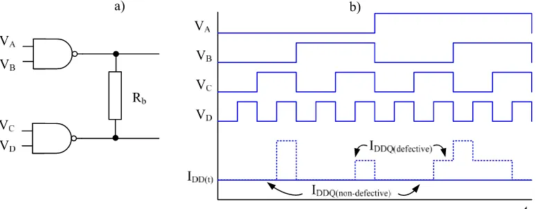
(33) 2 STATE OF THE ART. Figure 2.7. Resistive bridge between two NAND gates a) Gate level b) V-Rb characteristic.. A detailed analysis of the behaviour of bridging defects was presented by SarDessai and Walker in [12]. This work analysed five different bridging fault configurations, namely: a bridging fault between two primary inputs, between a primary input and a gate output, between two gate outputs, between two gates outputs driving the same gate and between two primary outputs. Based on the model for these five configurations, look-up tables can be constructed, where the information about the voltage on the bridged nets is stored for every vector. The detectable resistance interval [11] and the propagating path are also taken into account. Furthermore, it is also determined whether the bridging fault is detectable at the driven gate outputs based on their logic thresholds. In a more recent work carried out by Polian et al. [13], the critical resistance was calculated based on more accurate transistor models: the Fitted Model, which uses equations with free variables that are fitted in order to match actual SPICE data, and the Predictive Model, which is fully analytical and employs BSIM4 equations. The characterization of bridging faults can be also based on electrical current information instead of looking the logic behaviour [14]. The easiest model is the socalled simple IDDQ bridging fault model. It assumes that when the bridged nodes are set to the same logic value related to the defect free case, no extra current is added. However, when they have different logic values, a current path is created between power and ground and extra current is generated. An example is illustrated in Figure 2.8a. The inverter contains a bridge between the source and the gate of the pMOS transistor. When the inverter input (VA) is in a high logic state, the nMOS transistor is on. The current consumption is only due to leakage current, as described in Figure 2.8b. However, if VA transitions from logic 1 to logic 0, the nMOS transistor turns off and the pMOS transistor turns on. In the fault free case, once all the signals have settled-down, 11.
(34) 2.1 FAULT MODELS. the current consumption is again the leakage current. Nevertheless, due to presence of the bridge, during the low logic state of VA, there is current flowing from the source to the gate of the pMOS transistor, increasing the quiescent current value.. A. B A. B. DDQ(defective). DD(t) DDQ(non-defective). Figure 2.8. Bridge affecting the pMOS transistor of an inverter a) Gate level b) IDD(t).. The current behaviour of bridging faults can be more accurately described if the concept of the voting model is adapted to the current behaviour. Every network excitation is expected to add different currents values, as illustrated in Figure 2.9. The extra current depends on the number of pMOS transistors of the NAND gate in the on state when the bridge is excited. The extensive work carried out to characterize bridging faults has improved their models since their appearance. However, more research is still needed, since some cases have not been yet fully solved. Transistor parameters and bridge resistances are susceptible to process variation, which are difficult to predict and influence the behaviour of this class of faults. Feedback bridging faults are still difficult to detect. Furthermore, bridging faults involving more than two nets are not considered by present fault models.. Figure 2.9. Bridge affecting the outputs of two NAND gates a) Gate level b) IDD(t).. 12.
(35) 2 STATE OF THE ART. 2.1.2.3 FEEDBACK BRIDGING FAULTS A feedback bridging fault is a bridging fault such that both involved nets lie on the same path in the circuit [2]. The voltage value of one bridged net may depend on the value of the other bridged net. The bridged net with lower topological ordering is usually called the back net, while the other one is called the front net. The analysis of feedback bridging faults is complex. They can induce sequential behaviour in combinational circuits, depending whether the path is sensitized or not and depending also on the topological situation of the bridge. Thus, three different cases may appear [15]-[18]: 1. The logic path is not sensitized. 2. The logic path is sensitized and the feedback loop has an even number of inversions. 3. The logic path is sensitized and the feedback loop has an odd number of inversions. When the logic path is not sensitized, it is equivalent to a non-feedback bridging fault. The logic value of the back net is independent of the logic value of the front net. Considering the examples shown in Figure 2.10, this is accomplished as long as VC is set to logic 0. If the logic path is sensitized and the feedback loop has an even number of inversions, both nets have the same logic value. An example is illustrated in Figure 2.10a provided that VC is set to logic 1. This case is redundant as long as the back net is stronger than the front net, otherwise a circuit with asynchronous memory behaviour appears. It can be then described as a latched state. The voltage on the bridged nets depends on the transistor strengths and the bridge resistance. The detectability of such fault cases relies on the sequence of test patterns applied.. Figure 2.10. Feedback bridge a) Even number of inversions b) Odd number of inversions.. Finally, if the logic path is sensitized with an odd number of inversions, the logic values of the bridged nets are opposite on a fault-free circuit (see Figure 2.10b). Two different behaviours may appear depending on the gate strengths. If the back gate is stronger than the front gate, it behaves as a non-feedback bridging fault. However, if the front gate is stronger, the defect may cause oscillation in the circuit. The oscillation 13.
(36) 2.1 FAULT MODELS. period is related to the delay of the logic connecting the bridged nodes and it is usually lower than the clock period. The impact of the bridge resistance in feedback bridges is not a trivial issue, since it turns out to be computationally complex [19]. However, bridge resistances with high values usually result in fewer situations of active feedback because the dominance conditions of the front net are less likely to be accomplished. 2.1.2.4 GATE OXIDE SHORTS (GOS) Gate Oxide Shorts (GOS) may be considered as a particular class of bridging faults. GOS are intra-transistor bridges caused by hard transistor oxide breakdowns from particles or oxide imperfections [20]. In a defect-free transistor, the polysilicon gate is electrically isolated from the rest of terminals by means of a thin layer of silicon dioxide (SiO2). A GOS is a rupture in this silicon dioxide, connecting the gate terminal with one of the silicon structures beneath the oxide. The electrical properties of a GOS depend on their location, since there are three different regions to which the gate can be connected. In this way, a GOS may connect the polysilicon gate terminal with the drain, source or bulk of the device. Furthermore, the doping type of the connected silicon structures affects the electrical properties of the GOS. When the polysilicon gate and the diffusion are of the same doping type, the electrical characteristic of the junction is ohmic. However, when they are of different doping type, the electrical model is a pn junction diode between both terminals. The GOS fault model depends on the semiconductor structures taking part in the fault. From here on assume that the polysilicon gate doping is n-type, which has been the more common doping type for long-channel technologies. Anyway, the GOS behaviour with p-doped polysilicon gate can be deduced from the complementary behaviour assuming n-doped polysilicon gates. Therefore, the behaviour of a GOS between the p-doped polysilicon gate and the bulk of a pMOS transistor can be derived from the behaviour of a GOS between the n-doped polysilicon gate and the bulk of an nMOS transistor, as observed in Figure 2.11 [20]-[21]. An n-doped polysilicon gate to drain/source GOS in nMOS transistors generates an ohmic connection. The behaviour is similar to an external bridge between both terminals.. 14.
(37) 2 STATE OF THE ART. Figure 2.11. Electrical models for Gate Oxide Shorts [20]-[21].. A gate to bulk GOS present in nMOS transistors results in a diode with the anode at the bulk and the cathode at the gate. Under normal operation, the diode is expected to be reversed biased, adding negligible current. However, a parasitic nMOS transistor forms. The transistor with the GOS behaves in a similar way as two minor transistors connected in series with a resistance between the gates and the common terminal of both transistors. Figure 2.11 shows the equivalent electrical model for this case. A GOS defect between the gate and the source/drain of a pMOS transistor forms a parasitic diode between both terminals, being the gate the cathode and the source/drain the anode of the diode. On the one hand, a GOS to the source of the pMOS transistor clamps the gate voltage to a diode drop below VDD when the preceding stage is trying to set the gate to a low logic value. Otherwise, the diode is reverse biased, adding negligible current. On the other hand, the behaviour of a GOS to the drain of the transistor is more complicated. The diode acts as a feedback element from the drain to the gate of the transistor. In case of a GOS between the gate and the bulk of a pMOS transistor, a resistive ohmic contact forms. However, once the transistor is switched on, the parasitic GOS resistance allows base terminal current injection in the parasitic bipolar transistor. In this case, the gate current acts as the base current for the parasitic bipolar transistor. As GOS behaviour depends on its location, fault models considering its exact location have been developed. Sytrzycki [22] presented an approach which relies on designing the transistor physics-based model by means of lumped-elements. In this way, a non-defective channel is represented by a bi-dimensional array of MOS transistors. One can arbitrary choose the number and size of elements. The higher the number of elements, the most accurate the model. However, more computational effort is required. 15.
Figure


+7


![Figure 2.21. Matching algorithm [116].](https://thumb-us.123doks.com/thumbv2/123dok_es/5264993.96700/56.595.201.391.86.240/figure-matching-algorithm.webp)

Documento similar
In the preparation of this report, the Venice Commission has relied on the comments of its rapporteurs; its recently adopted Report on Respect for Democracy, Human Rights and the Rule
Case 1: If the solution of the Riemann problem consists of a 1-shock and a 2-rarefaction waves: the cell is marked. Case 2: If the solution of the Riemann problem consists of
De esta manera, ocupar, resistir y subvertir puede oponerse al afrojuvenicidio, que impregna, sobre todo, los barrios más vulnerables, co-construir afrojuvenicidio, la apuesta
In the “big picture” perspective of the recent years that we have described in Brazil, Spain, Portugal and Puerto Rico there are some similarities and important differences,
In our proposal we modeled the problem using a Markov decision process and then, the instance is optimized using linear programming.. Our goal is to analyze the sensitivity
In the previous sections we have shown how astronomical alignments and solar hierophanies – with a common interest in the solstices − were substantiated in the
Díaz Soto has raised the point about banning religious garb in the ―public space.‖ He states, ―for example, in most Spanish public Universities, there is a Catholic chapel
teriza por dos factores, que vienen a determinar la especial responsabilidad que incumbe al Tribunal de Justicia en esta materia: de un lado, la inexistencia, en el
