1
Active and hybrid filters in medium voltage distribution power systems
V.F. Corasaniti
1M.B. Barbieri
1P.L. Arnera
1M.I. Valla
21
Instituto de Investigaciones Tecnológicas para Redes y Equipos Eléctricos (IITREE-LAT)
2
Laboratorio de Electrónica Industrial Control e Instrumentación (LEICI) Facultad de Ingeniería. Universidad Nacional de La Plata
Argentina
SUMMARY
This paper presents the design of different topologies of active power filters to compensate reactive power and harmonics in the medium voltage level of a distribution power system. One pure active filter and two hybrid topologies, are implemented. A pure active compensation is obtained with a Shunt Active Power Filter (SAPF). The shunt combination of SAPF and passive filter, form one of the hybrid topologies implemented, named Shunt Hybrid Active Power Filter (SHAPF). The other hybrid topology, called Hybrid Shunt Active Power Filter (HSAPF), connects the active filter in series with two shunt passive filters. The control algorithm are implemented with the d-q theory measuring the system current to compensate the load, setting a feedback control loop, rather than a simple feedforward compensation. Simulation for different load demands and distortions are performed. Finally a comparative evaluation of the different filters is carried out.
KEYWORDS
Distribution Power System - Reactive Power - Harmonic - Power Quality - Active Power Filter.
21, rue d’Artois, F-75008 PARIS
B4_201_2010
CIGRE 2010
2
1. INTRODUCTION
Non-linear loads and equipments in the consumer side and renewable energy sources in the generation side are defining the need of power electronics as an essential interface in power systems to improve Power Quality [1]. Voltage distortion, due to current harmonics, has become a major problem for the utilities at distribution levels. Utilities frequently encounter harmonic related problems, such as higher transformers and line losses, reactive power, and resonance problems, de-rating of distribution equipment, harmonic interactions between the utility and loads, reduced system stability and reduced safe operating margins [1] [2].
The use of traditional compensation with capacitor banks and passive filters gives rise to harmonic propagation. That is harmonic voltage amplification due to resonance between line inductances and shunt capacitors. So, different active solutions have been continuously analyzed in the last years [3]-[7]. A lot of research has been followed on different topologies to improve Power Quality [8][9].
Among all this compensation alternatives the hybrid topologies which use passive and active filters result very attractive in distribution power systems where some passive compensation is already installed [10]-[13]. Such a combination between active and passive filters allows reducing significantly the rating of the active filter, since its main task is to improve the filtering performance and to avoid the resonance problems introduced by passive filters. In this way it constitutes a simple and cheap solution for harmonics in distribution power systems.
A particular problem of an actual distribution substation (DS) is considered in this paper. This paper proposes different control algorithm based in the synchronous reference frame (d-q) with a feedback control, rather than (p-q) theory with load feedforward compensation. It is applied to the design of different topologies of active filters. Three active topologies connected to the medium voltage level of DS (SAPF, SHAPF and HSAPF) are proposed here to solve the particular problem of reactive power and harmonics compensation.
2. SYSTEM DESCRIPTION
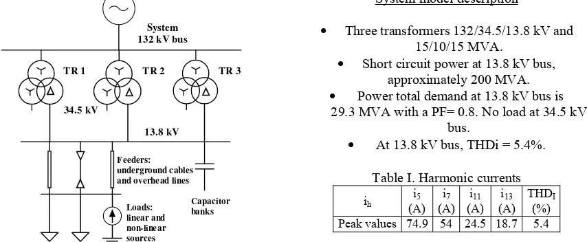
[image:2.595.95.268.483.667.2]The 132 kV system, where the DS under study is connected, works meshed and connected to the 500 kV high voltage transmission system. Inthe future, the requirement to enhance the voltage profile at 13.8 kV level demands for new compensation in the different substations [14].
Fig. 1 shows the one line diagram of the system model adopted for the DS under test.
System 132 kV bus
13.8 kV 34.5 kV
Capacitor banks Feeders:
underground cables and overhead lines
TR 1 TR 2
Loads: linear and non-linear sources
TR 3
Fig. 1. One line diagram of system model.
System model description
• Three transformers 132/34.5/13.8 kV and
15/10/15 MVA.
• Short circuit power at 13.8 kV bus,
approximately 200 MVA.
• Power total demand at 13.8 kV bus is
29.3 MVA with a PF= 0.8. No load at 34.5 kV bus.
[image:2.595.95.522.489.665.2]• At 13.8 kV bus, THDi = 5.4%.
Table I. Harmonic currents
ih
i5 (A)
i7 (A)
i11 (A)
i13 (A)
THDI (%)
Peak values 74.9 54 24.5 18.7 5.4
The system is represented as an ideal voltage source of 132 kV connected to three transformers. The system is modeled by an equivalent impedance related to short circuit power at 13.8 kV. All transformers are connected in parallel to 13.8 kV where the capacitor banks and the loads are placed. Feeders, underground cables and overhead lines, are considered at the load connection.
3
sources with amplitude and frequency corresponding to each harmonic. The power total demand and the harmonics currents shown in Table I, considered in this model, are based on the power flow and harmonics studies performed on the system [14].
A reactive compensation of 9.6 Mvar will result in PF = 0.94 at 13.8 kV bus system which is the goal for the proposed compensator. Compensation of the reactive currents with capacitors banks of 4.8 Mvar gives rise to parallel resonances which increase the harmonics to unacceptable levels. The results of this compensation, together with P and Q, and the reactive power provided by capacitor banks (QAC) and the current and voltage distortion, are summarizes in Table II.
Table III summarizes the harmonic voltages and THDV for all cases together with the allowable
limits fixed by IEC [15]. For QC = 4.8 Mvar and QC = 9.6 Mvar cases, the individual harmonic
voltages for the 5th and the 7th harmonics and THDV are above the allowable limits, so a different
compensation should be considered.
Table II. System results
QC (Mvar)
P (MW)
Q (Mvar)
V1 phase
(kV rms)
THDV (%)
I1 line
(A rms)
THDI (%)
0 23.4 17.7 7696 5.66 1269 5.43
4.8 24.4 13.7 7865 9.65 1188 10.7
9.6 25.5 9.7 8040 9.64 1129 13.8
Table III. Harmonic voltages verifications Harmonic
voltages QC (0 Mvar)
QC (4.8 Mvar)
QC (9.6 Mvar)
IEC limits
V5 (%) 3.29 5.47 8.88 6
V7 (%) 3.32 7.48 3.61 5
V11 (%) 2.37 2.30 0.86 3.5
V13 (%) 2.14 1.42 0.56 3
THDV (%) 5.66 9.65 9.64 8
3. PURE ACTIVE FILTER
One of the most popular topologies employed in harmonic compensation is the Shunt Active Power Filter (SAPF) [16]. A general structure of the Shunt Active Power Filter (SAPF) is presented in Fig. 2.
Control
algorithm CurrentControl
Vdc voltage regulator
i Fa i Fb i Fc i* Ca
i* Cb i* Cc i Sa
i Sb i Sc
Va Vb Vc
ωst
PLL Vdc
Ripple filter (damped) Transformer
a
b c
Coupling inductor Inverter
i Fa
i Fb
i Fc Vc
Vb
Va Linear
and non-linear
load a
b c
i La
i Lb
i Lc
i Sa
i Sb
[image:3.595.172.440.393.610.2]i Sc
Fig. 2. General structure of the implemented SAPF.
In this case, the whole compensation is performed by the SAPF. The current harmonics are completely provided by the SAPF, while the reactive compensation is limited to 9.6 Mvar which is the goal for the proposed compensator and limits the current delivered by the SAPF.
4
The CCVSI is a standard two level three phase voltage source inverter with IGBTs [1] [3]. The current loops are closed with hysteresis controllers. The output current through the coupling inductor is sampled at a fixed frequency in order to limit the switching frequency of the inverter. Its mean value is approximately equal to 10 kHz. The switching frequencies are further filtered with a second order damped parallel filter which takes the high frequency currents away from the system [2].
The DC side capacitance is selected in order to keep the voltage ripple below 2 %. The DC value is chosen so that the converter can supply the current time derivatives demanded by the harmonics to be compensated. Finally the coupling transformer adapts the voltage level of the power system (13.8 kV) to AC voltage obtained from the CCVSI with a 6.5 kV on the DC side.
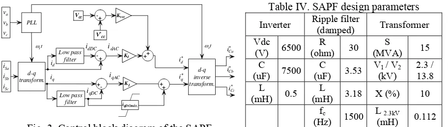
The control system measures the line currents of the three-phase system (iSa, iSb, iSc). Then they are
transformed into the active (id) and reactive (iq) components using a reference system synchronous
with the positive sequence voltage of the fundamental frequency of the system [3]. The phase of this sequence is provided by a Phase Locked Loop (PLL). The active and reactive currents can be also decomposed in their DC and AC values. The mean values of the active and reactive currents (idDC) and
(iqDC) are the fundamental active and reactive current components, while the AC components of both
currents (idAC) and (iqAC) correspond to the contribution of active and reactive harmonics components
and the negative sequence of the load currents.
It is desired that the system supplies the DC value of the active current (idDC) while its AC
component (idAC) as well as the whole reactive current (iq) are supplied by the SAPF. Then, the
instantaneous active and reactive currents are filtered in order to separate both components and generate the correct reference to the CCVSI, (i*d) and (i*q). These current components are amplified
by a gain KI to obtain the references to the power inverter.
Besides providing the harmonic currents, the control system should maintain the DC voltage of the CCVSI to guarantee its accurate operation. So the DC voltage control is obtained controlling (id) as
shown in Fig. 3, where the diagram of the control system is presented.
c b a v v v PLL d-q transform. Sc Sb Sa i i
i id
q i Low pass filter Low pass filter -+ -+ KI KI t s
ω ωst
∗ d i ∗ q i dDC
i idAC
qAC i qDC i + + -+
Vcc Kvcc
[image:4.595.70.526.416.546.2]+ + ∗ Ca i ∗ Cb i ∗ Cc i iqDCmáx. V* cc d-q inverse transform.
Fig. 3. Control block diagram of the SAPF.
Table IV. SAPF design parameters
Inverter Ripple filter
(damped) Transformer
Vdc
(V) 6500
R
(ohm) 30
S
(MVA) 15
C
(uF) 7500
C
(uF) 3.53
V1 / V2 (kV)
2.3 / 13.8 L
(mH) 0.5
L
(mH) 3.18 X (%) 10
fc
(Hz) 1500
L 2.3kV
(mH) 0.112
The proposed control eliminates the AC components of the active current (idAC). This means the
oscillating part of the active power. Regarding the reactive power component, the implemented control compensate the AC components of the reactive current (iqAC) plus a part of the mean value of the
reactive current (iqDC), limit to (iqDCmáx.) which corresponds to Qmax = 9.6 Mvar.
The phase current of the inverter (iFa, iFb, iFc) are compared, one by one, with the current reference
(i*Ca, i*Cb, i*Cc) through three hysteresis comparators, to generate the trigger signals to the inverter.
The phase current of the inverter are sampled at a fixed frequency for the purpose of limiting the maximum switching frequency. The hysteresis control with limited frequency is simple, fast and robust. The design parameters of SAPF are summarized in Table IV.
4. HYBRID SHUNT-SHUNT FILTER
A general structure of the Shunt Hybrid Active Power Filter (SHAPF) [16] is presented in Fig. 4. It is formed connecting a shunt passive filter to the same general structure of SAPF shown in Fig. 2.
5
Then, 4.8 Mvar are compensated by the passive filter and less current is provided by the SAPF. It also supplies the harmonics that are not provided by the passive filter.
The design of the active filter is the same of the above presented pure active topology. In this topology, the limit (idDCmáx.) is changed to the corresponding with Qmax = 4.8 Mvar Since the SAPF
works with lower current, a smaller capacitance is required to maintain the same value of ripple of the DC voltage. The SAPF and the connection transformer are designed for a smaller power, as shown in Table V. The passive filter consists of simple LC filter per phase tuned at 5th harmonics and 4.8 Mvar of reactive power [3].
The design parameters of SHAPF are summarized in Table V. The ripple filter parameters are the same that were presented in Table IV.
Linear and non-linear
load a
b
c
i La i Lb i Lc i Sa
i Sb i Sc
i Sa i Sb i Sc
Va Vb Vc
SAPF
Passive filter (tuned) System
[image:5.595.76.302.217.318.2]Fig. 4. General structure of the implemented SHAPF
Table V. SHAPF design parameters
Inverter Transformer Passive filter
Vdc
(V) 6500
S
(MVA) 10
Q
(Mvar) 4.8
C
(uF) 3000
V1/V2 (kV)
2.3/ 13.8
R
(ohm) 0.17
L
(mH) 0.5
X
(%) 10
C
(uF) 80.2
L2.3kV
(mH) 0.168
L
(mH) 5.05
5. HYBRID SHUNT-SERIE FILTER
A general structure of the Hybrid Shunt Active Power Filter (HSAPF) [10], is presented in Fig. 5.
Passive filters (tuned)
Vdc voltage regulator
Va Vb Vc
Control
algorithm PWM PLL
ωs t i Sa
i Sb i Sc
V* ca V* cb V* cc
ωs t
Vdc Ripple
filter (damped)
a
b c
Inverter
V ca V cb V cc
Vc Vb
Va Linear
and non-linear
load a
b c
i La i Lb i Lc i Sa
[image:5.595.168.441.390.574.2]i Sb i Sc
Fig. 5. General structure of the implemented HSAPF
It consists of a three phase pulse width modulation (PWM) voltage source inverter (VSI) connected in series with one or more passive filters. They are directly connected to the system without the need of a transformer. The passive filters consist of simple LC filters per phase tuned at certain harmonic frequencies. In the same way as in SAPF and SHAPF, the switching frequencies are further filtered with the same second order parallel filter.
Basically, the active power filter acts as a controlled voltage source which forces the system line currents to become sinusoidal. The voltage references for the VSI are generated by the control system based on the d-q transformation as in the SAPF and SHAPF topologies, and a close loop control of the DC voltage. The active filter is used only to compensate harmonics while the 9.6 Mvar of reactive currents are damped by the passive filters.
6
provide 4.8 Mvar each. The reasons for this selection are: 1) the LC filter tuned at the 7th and 11th harmonic frequency is less bulky and less expensive than one tuned at the 5th and 7th harmonic frequency, 2) the filter tuned at the 11th harmonic presents lower impedance at the 13th harmonic than other tuned at the 7th harmonics. The passive filters are designed in the same way that in SHAPF topology [3]. Table VI summarizes the parameters of the passive filters.
The PWM Voltage Source Inverter is a standard two level three phase voltage source inverter with IGBTs using a standard sinusoidal modulation with a carrier frequency of 10 kHz. The DC side of the converter is built only with a capacitor of proper value. The capacitance is selected in order to keep the voltage ripple below 2 %. The DC value is chosen so that the converter can supply the current time derivatives demanded by the harmonics to be compensated. The active filter can build up and regulate the DC voltage on the capacitor without any external power supply or special start up circuit. The inverter design values are: Vdc= 1500 V and Cdc = 3000 uF.
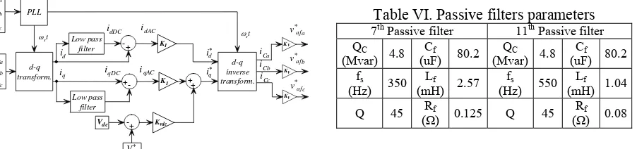
The control system is shown in Fig. 6. The three-phase supply currents (iSa, iSb, iSc), the three-phase
supply voltages (Van,Vbn,Vcn) and the DC voltage of the inverter are measured, to build the reference
voltages for the PWM VSI. It is desired that the system supplies the DC value of the active current while its AC component as well as the whole reactive current are supplied by the HSAPF. Considering the reactive current, its DC value is supplied by the passive filter while the VSI provides an AC voltage to damp the harmonics. Then, the instantaneous active and reactive currents are filtered in order to separate both components and generate the correct reference to the PWM modulator. These current components, (idAC) and (iqAC), are amplified by a gain KI to obtain the references to the power
inverter.
Besides providing the harmonic currents, the control system should maintain the DC voltage of the PWM VSI to guarantee its accurate operation. It is important to notice that no active fundamental current flows through the LC filter. So the DC voltage control is obtained controlling (iq) as shown in
Fig. 6, where the diagram of the control system is presented.
Each current component is amplified by a gain KV which corresponds to the voltage gain of the
PWM Inverter. The resultant signal (vaf*) correspond to the phase voltages which should be
synthesized by the power inverter.
c b a v v v PLL d-q transform. Sc Sb Sa i i
i id
q i Low pass filter Low pass filter -+ -+ KI
KI ++
-+
Vdc Kvdc
d-q inverse transform.
t s
ω ωst
KV KV KV ∗ d i ∗ q i ∗ dc V dDC i qDC i dAC i qAC i Ca i Cb i Cc i b af v* c af v* a af v*
[image:6.595.77.528.465.571.2]Fig. 6. Control block diagram of the HSAPF.
Table VI. Passive filters parameters
7th Passive filter 11th Passive filter
QC
(Mvar) 4.8
Cf
(uF) 80.2
QC
(Mvar) 4.8
Cf
(uF) 80.2
fs
(Hz) 350
Lf
(mH) 2.57
fs
(Hz) 550
Lf
(mH) 1.04
Q 45 Rf
(Ω) 0.125 Q 45
Rf (Ω) 0.08
6. PERFORMANCE EVALUATION
The proposed filter topologies to compensate the DS under study are evaluated and compared in this section. The DS and filters are simulated for different load conditions. First a load and distortion equal to the 50 % of maximum demand is considered. Afterwards, the load and the harmonic distortion are increased to the maximum demand.
First the steady state compensation is considered. The three implemented topologies are compared with regards to the line voltage and current upstream the filters. The final stage of maximum demand and 9.6 Mvar reactive compensation are presented.
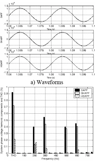
Fig. 7 a) shows the system line current waveforms at 13.8 kV bus (upstream the filters), while Fig. 7 b) presents the harmonic components together with the THDI. The equivalent results
7
a) Waveforms
b) Harmonic components and THDI.
Fig. 7. System line currents of 3 topologies.
a) Waveforms
b) Harmonic components and THDV.
Fig. 8. System phase voltages of 3 topologies.
The results of Figs. 7 and 8 show a decrease of the current and voltage harmonics and the THD with respect to compensation with capacitor banks. This is confirmed in Table VII when compared to the last row of Table II. Here the variables of the three filter topologies are presented. Both THDV and
THDI have been calculated considering up to the 50th order harmonics. When the harmonic order is
increased up to 12 kHz, in order to consider the commutation frequency, the THDV increases to 2 % in
[image:7.595.85.272.66.371.2]the SAPF and SHAPF topologies and to 0.4 % in the HSAPF, while the current distortions remain almost the same in all topologies.
Table VIII summarizes the voltage harmonics and THDV for the 3 topologies with the allowable
limits like in Table III for capacitor banks. The individual harmonic voltages and THDV are well
below the allowable limits.
Some simulations were developed to evaluate the behavior of the filter in presence of negative sequence fundamental load currents. Here certain unbalanced load is characterized by a 7 % negative sequence load current (ratio of negative sequence current to positive sequence current) added to the reactive and harmonics shown in the previous subsection. The current of each phase at the 13.8 kV level upstream the SAPF and SHAPF, are presented in Figs. 9 a) and b). The SAPF and SHAPF are connected at t=0.2 s to compensate reactive power, harmonics and unbalance. Figs. 9 a) and b) show how the unbalanced currents in each phase became almost balanced. The 7 % negative sequence load current of originally considered, was reduced to 0.6 %.
The HSAPF is not suitable for unbalanced compensation, since this requires fundamental voltage generation. To obtain this is it necessary to increase the DC voltage and power rating of the inverter, loosing its main advantage.
[image:7.595.334.517.67.378.2]8
Table VII. System results
Topol. P
(MW) Q (Mvar)
V1 phase (kVrms)
THDV (%)
I1 line (Arms)
THDI (%)
SAPF 25.8 9 8057 0.92 1131 0.91
SHAPF 25.8 9 8060 0.72 1130 0.62
HSAPF 25.6 9.4 8042 0.22 1133 0.27
Table VIII. Harmonic voltages verifications Harmonic
voltages SAPF SHAPF HSAPF
IEC limits
V5 (%) 0.4 0.12 0.17 6
V7 (%) 0.55 0.43 0.07 5
V11 (%) 0.4 0.38 0.02 3.5
V13 (%) 0.45 0.4 0.05 3
THDV (%) 0.92 0.72 0.22 8
a) SAPF unbalanced compensation
b) SHAPF unbalanced compensation
Fig. 9. Unbalanced currents compensation.
a) Waveforms
b) Fundamental and harmonic components. Fig. 10. Filter current components of 3 filters.
[image:8.595.87.399.86.530.2]The three filters show very good performances. Regarding their complexity and component count Table IX summarizes the requirements of the three topologies.
Table IX. Summary of topologies components
Components SAPF SHAPF HSAPF
S = √3 /2 .VDC. Ipeak (MVA) 26 15 1
IGBT rating
Current (A peak) 4600 2600 800
Voltage (V) 6500 6500 1500
Inverter
DC capacitor
C (uF) 7500 3000 3000
Coupling inductor yes yes no
Connection transformer (MVA) 1 x 15 1 x 10 no
Passive filter (Mvar) no 1 x 4.8 2 x 4.8
[image:8.595.111.487.606.733.2]9
7. CONCLUSIONS
The design of a three topologies of shunt active or hybrid filters to compensate reactive power and harmonics in the medium voltage level of a power distribution system were presented and compared in this paper. The first topology considered full compensation with the active filter; the second one used the existing capacitor bank and built the complementary compensation with the active filter, while the third one considers the active filter in series with 2 passive filters. The synchronous reference frame (d-q) and the control loop feedback, show very good performance in the three proposals. The last topology results in a more economic solution in particular when there is some passive compensation already included in the distribution system. It is rather simple and it presents a very good performance in transient and steady state operation.
BIBLIOGRAPHY
[1] E. Acha, V.G. Agelidis, O. Anaya-Lara, T.J.E. Miller, Power Electronic Control in Electrical Systems, Newnes Power Engineering Series, 2002.
[2] J. Arrillaga, N. R. Watson, Power System Harmonics, 2nd ed., Wiley & Sons Ltd., 2003.
[3] H. Akagi, E. Watanabe and M. Aredes, Instantaneous Power Theory and Applications to Power Conditioning, IEEE Press Series on Power Engineering, 2007.
[4] Gerbex, S; Orzan D; Oudalov A; Cherkaoui R; Germond A.J: Optimal location and coordinated control of FACTS devices in the Swiss power system. CIGRE Session 2004, Paper B4-205. [5] Talaat Abu El-Fetoh, “Harmonic Intelligent Control with Active Power Filter”, Proceedings of
the 19th International Conference CIRED 2007.
[6] W. Gawlik, “Optimal Placement and Mutual Influence of Active Filters”, Proceedings of the 17th International Conference CIRED 2003.
[7] M.Z. El-Sadek, M.A.A. Wahab, M. Hamada, M. R. Ghallab, “Suggested Hybrid Active Power Filter for Damping Harmonic Resonance in Power Distribution Systems”, Proceedings of the 19th International Conference CIRED 2007.
[8] A. Huang, S. Bhattacharya, M. Baran, B. Chen, C. Han, " Active Power Management of Electric Power System Using Emerging Power Electronics Technology," in Proc.2007 IEEE PES general meeting Conf., pp.1-7.
[9] Pazos, F.J., Amezua, A., Gutierrez, I., Garcia, J.M., Buigues G., Gracenea, I.: New Active Earthing System for Distribution Networks by Means of Power Electronics. CIGRE Session 2008, Paper B4-306.
[10] V.F. Corasaniti, M.B. Barbieri, P.L. Arnera, M.I. Valla, “Hybrid Power Filter to Enhance Power Quality in a Medium Voltage Distribution Network” IEEE Transactions on Industrial Electronics, Vol. 56, NO. 8, pp. 2885-2893, August 2009.
[11] R. Inzunza and H. Akagi, “A 6.6-kV Transformerless Shunt Hybrid Active Filter for Installation on a Power Distribution System” IEEE Trans. Power Electronics, vol. 20, No. 4, pp. 893-900, July 2005.
[12] D. Rivas, L. Morán, J. Dixon and J. R. Espinoza, "Improving Passive Filter Compensation Performance With Active Techniques," IEEE Trans. Industrial Electronics, vol. 50, No. 1, pp. 161-170, Feb. 2003.
[13] S. Srianthumrong and H. Akagi, "A Medium-Voltage Transformerless AC/DC Power Conversion System Consisting of a Diode Rectifier and a Shunt Hybrid Filter," IEEE Trans. Industry Applications, vol. 39, No. 3, pp. 874-882, May/Jun 2003.
[14] V. F. Corasaniti, M. B. Barbieri, P. L. Arnera and M. I. Valla, "Load characterization in Medium Voltage of an Electric Distribution Utility Related to Active Filters," in Proc.2006 IEEE PES TDC Conf., ISBN:1-4244-0288-3.
[15] IEC 61000-2-12. Electromagnetic Compatibility (EMC). Part 2. Section 12: Compatibility levels for low-frequency conducted disturbances and signalling in public medium-voltage power supply systems.