453
Mikhail Soloviev (ed.), Nanoparticles in Biology and Medicine: Methods and Protocols, Methods in Molecular Biology, vol. 906, DOI 10.1007/978-1-61779-953-2_37, © Springer Science+Business Media, LLC 2012
Chapter 37
Scanning Transmission Electron Microscopy Methods
for the Analysis of Nanoparticles
Arturo Ponce , Sergio Mejía-Rosales , and Miguel José-Yacamán
Abstract
Here we review the scanning transmission electron microscopy (STEM) characterization technique and STEM imaging methods. We describe applications of STEM for studying inorganic nanoparticles, and other uses of STEM in biological and health sciences and discuss how to interpret STEM results. The STEM imaging mode has certain bene fi ts compared with the broad-beam illumination mode; the main advantage is the collection of the information about the specimen using a high angular annular dark fi eld (HAADF) detector, in which the images registered have different levels of contrast related to the chemical composition of the sample. Another advantage of its use in the analysis of biological samples is its contrast for thick stained sections, since HAADF images of samples with thickness of 100–120 nm have notoriously better contrast than those obtained by other techniques. Combining the HAADF-STEM imaging with the new aberration correction era, the STEM technique reaches a direct way to imaging the atomistic structure and composition of nanostructures at a sub-angstrom resolution. Thus, alloying in metallic nanoparticles is directly resolved at atomic scale by the HAADF-STEM imaging, and the comparison of the STEM images with results from simulations gives a very powerful way of analysis of structure and composition. The use of X-ray energy dispersive spectroscopy attached to the electron microscope for STEM mode is also described. In issues where characterization at the atomic scale of the interaction between metallic nanoparticles and biological systems is needed, all the associated techniques to STEM become powerful tools for the best understanding on how to use these particles in biomedical applications.
Key words: Scanning transmission electron microscopy , STEM , Inorganic nanoparticles , Biological systems , HAADF-STEM , Aberration-corrected microscopy
Conventional transmission electron microscopy (TEM) is a beam characterization technique with almost 80 years since the develop-ment of the fi rst microscope. In TEM, a large area of the specimen is illuminated, the magni fi cation is performed by the lens system underneath the specimen, and subsequently the whole image is registered instantaneously. Conventional scanning electron
modes, STEM or TEM, so there is a tendency to discard the use of dedicated instruments. One of the main advantages of the STEM over the TEM is that the signal generated by the electrons scattered out to high angles on a high-angle annular dark fi eld detector (HAADF), is chemically sensitive, and a sample with a de fi nite crystalline arrangement is not necessarily a requirement. The capacity of STEM of generating these different levels of con-trast is commonly known as Z-concon-trast; the concon-trast dependance goes approximately as Z 2 , Z corresponding to the atomic weight
of the element that caused the scattering of the electrons ( 1 ) . For nanostructures, TEM and STEM operational modes become necessary due to the fact that matter properties from bulk can result in different—sometimes even improved—properties at the nanoscale from those at bulk. This dependence in size is due to several reasons: quantum effects, surface effects, and modi fi cation of thermal behavior, among others ( 2, 3 ) . In order to take advan-tage of the physical and chemical properties of the nanostructures by guiding the fi ne-tuning of these properties depending on the purposes for which the structures has been created, a deep under-standing on the relation between shape, size, and function, is needed. The appropriate generation and interpretation of electron micrographs is crucial for this purpose. The interpretation of the electron micrographs is not always straightforward, since the inten-sity signal that correlates with the atomic positions depends not just in the length of the atomic columns parallel to the direction of the electron beam, but also on the chemical species, and on the microscope’s parameters at which the micrograph was obtained ( 4 ) . In this way, the problem of extracting a third dimension from the information contained in a strictly two-dimensional image requires the comparison of the observed images against simple models acquired by previous experience or inherited, and in many cases a theoretical model of the structure is necessary.
455 37 Scanning Transmission Electron Microscopy Methods…
concentrate in the use of STEM imaging. The chapter aims to be a guide for researchers interested in the characterization, at atomic scale, of metallic nanoparticles, and nanostructures. We will cover the working principles of STEM, the role of aberration correctors, and how the theory supporting the imaging of micrographs can be used to simulate the imaging process, to concentrate later on the practical issues concerning the comparison and interpretation of real and simulated electron micrographs of nanostructures.
In TEM, the information transfer in phase contrast imaging is determined by the objective lens and the size of it aperture, which are directly related to the temporal and spatial coherence of the electrons. In Fig. 1 , a conventional high resolution transmission electron microscopy (HRTEM) micrograph of a bimetallic nano-particle of 2 nm of diameter shows the interatomic distances; however, the contrast is not directly related with the different atomic positions in the bimetallic nanoparticle ( 5 ) proposed by the theoretical model shown in Fig. 1b . The optical arrangement of a conventional TEM compared with the STEM con fi guration is illustrated in the schematic diagrams shown in Fig. 2 . The scat-tered electrons in STEM mode can be regisscat-tered by three different detectors. The bright fi eld (BF) detector collects the electrons transmitted in the path of the beam close to the optical axis, the BF electrons containing the total beam current. The annular dark fi eld (ADF) and the HAADF detectors are used to record the electrons scattered out of the path of the beam. From the point of view of
2. Stem Imaging
the reciprocity theorem, the STEM is optically equivalent to an inverted TEM, in the sense that if the source and the detector exchange positions, the electron ray paths remain the same ( 6 ) . In the STEM, the objective lens—and all the relevant optics—are positioned before the specimen. The scattered angle of the ADF detector is set around ~40 mrad, and the outer angle is set around 60–200 mrad (see Fig. 2 ). STEM differs from conventional TEM in that the electron beam interacts only with a small section of the sample; the scanning process is the one in charge of generating the image as a whole, while in TEM, a broad beam is interacting instantaneously with the sample. X-ray energy dispersive spectros-copy (EDS) attached to the STEM mode provides with an elemen-tal analysis directly from the point or line raster-scanned in the sample. Therefore, the imaging using the BF or HAADF detectors in a complementary way can be matched to the EDS information, and the elemental mapping at atomic resolution is obtained. Figure 3 shows the setup of the STEM mode including the detec-tors a set of the detecdetec-tors typically used in STEM mode. Both the HAADF and BF detectors are shown in the picture. Examples of HAADF and BF images are included in Fig. 3 (on the right); both can be acquired simultaneously. L corresponds to the camera
length, which is the effective distance or magni fi cation between the specimen and the detector plane position. The X-ray detector is also shown in Fig. 3 ; the spectra can be collected at the same time together with STEM images. An example of the use of EDS and HAADF/BF-STEM is illustrated in Fig. 4 , where a set of
457 37 Scanning Transmission Electron Microscopy Methods…
STEM images from a bacterium show high contrast due to the presence of terbium inside and in the periphery of cells, which con fi rms the incorporation of Tb and indicates that TATA-binding protein (TBP) was mainly located in the periplasmic region. For HAADF images, the high contrast corresponds to the Tb incorpo-ration in the bacteria. The EDS spectrum obtained in a transversal region of bacteria is shown in Fig. 5 .
Fig. 3. STEM setup including the energy dispersive spectroscopy (EDS) spectrum detector.
The basic parameters described in this section are used to register high resolution STEM images. The process must be initialized in TEM mode for searching fi eld of view and adjust the crystal orien-tation if necessary. The eucentric focus must be adjusted with the z-control. By following the TEM initial setup, the system can be switched to STEM. The illumination focused on the sample must be adjusted by the size of the condensed aperture, spot size, and camera length ( L ). The camera length is the effective distance or magni fi cation between the specimen and the detector plane posi-tion (labeled in Fig. 2 ). The collection angle depends on the micro-scope camera length. Typical values for ADF and HAADF detectors vary from ~40 and 200 mrad, respectively.
The resolution in STEM depends upon the spot size of the electron beam. Both spot size and the aperture of the condenser lens have in fl uence in the beam current density in the sample and as consequence, in the resolution of the instrument. The beam current density in the sample can be increased by a large aperture of the condenser lens or by using a lower spot size. Figure 6 shows two different settings for STEM. Increasing the spot size (spot number) leads to increased demagni fi cation of the source and a decreased current in the beam. Increasing the spot number leads to a reduction of the beam current. Changing the size of the condenser lenses CL1 and CL2, produces that the beam current is also changed. In Fig. 7 , the sketches for the rays using two differ-ent sizes of the condenser apertures are illustrated. The selected aperture must be centered in the Ronchigram (described in next section) as is shown in Fig. 7 . Spot size and aperture of the
3. Practical
Considerations
for Stem Imaging
459 37 Scanning Transmission Electron Microscopy Methods…
condenser lens determine the resolution of the microscope in STEM mode. The spot size, measured in nanometers, can be simu-lated as a function of the parameters of the microscope ( 7 ) .
A Ronchigram is actually a shadow image, referring to the features at the center of the convergent beam electron diffraction (CBED) pattern, and formed by a focused and stationary electron probe on
4. The Ronchigram
amorphous material. The quality and resolution of the STEM images depend directly on the proper alignment of the Ronchigram. It is easily observable in fi eld emission gun (FEG) microscopes, but it might be dif fi cult to obtain in the Lanthanum Hexaboride (LaB 6 ) fi laments because the effective probe size is too large, and there-fore both the spatial resolution and the brightness decrease dra-matically, even using microscopes with voltages higher than 200 kV. All the parameters used to adjust different sets of contrast, spatial resolution, etc. are directly related with the Ronchigram. The Ronchigram can be registered in a CCD camera. The electrons coming out of the sample can be observed directly in a circle called the Gabor hologram , the Ronchigram or the central zero-order disk of the CBED pattern. The Ronchigram from an amorphous region should look as in the Fig. 8 . The Ronchigram is actually a shadow image, referring to the feature within the central disk of a CBED pattern and formed by a small, focused, and stationary probe on thin amorphous region. The optimal defocus is useful to optimize the spatial resolution and it can be corrected from the Ronchigram. When a near-focused beam illuminated on the specimen, the Ronchigram changes with the illumination conditions. In under and overfocus, an image of the sample is observed. Overfocus, in-focus, and underfocus Ronchigrams and the beam incident on the sample are illustrated in Fig. 9 . The shape of the Ronchigram can be simulated using the parameters of the microscope ( 7 ) .
461 37 Scanning Transmission Electron Microscopy Methods…
Electron microscopy has been improved greatly since 1990s with the correction of the spherical aberration and the chromatic aberration and is now capable of sub-angstrom resolution ( 1 ) . Another important aberration to be corrected is the axial coma. The coma astigmatism occurs when the direction of illumination does not coincide with the direction of the true optical axis of the elec-tron microscope. To reduce the effect of comma aberration in STEM, the beam must to be centered in the center in underfocus and overfocus conditions. The center of the Ronchigram must be positioned at the same point. Misalignment in X and Y direction can be observed in the Fig. 10 . The corrected X and Y directions of the comma astigmatism are observed in the center of the Ronchigram illustrated in the Fig. 10 . Astigmatism of the condenser lens must be aligned in X and Y directions. Non astigmatic Ronchigram and induced X and Y astigmatism are shown in Fig. 11 .
Fig. 9. Ronchigrams recorded with an underfocus, optimal defocus and overfocus electron probe on an amorphous specimen.
463 37 Scanning Transmission Electron Microscopy Methods…
HAADF image resolution is primarily determined by the size of the illumination probe, which is formed by the condenser system of the microscope. The best probe is formed at a balance of resolu-tion (narrow illuminaresolu-tion peak) and contrast (minimal tails), which means aperture semi-angle of (4 l /Cs) 1/4 and defocus of −( l /
Cs) 1/2 . The resolution of incoherent STEM and TEM image will
then be:
1/ 4 3/ 4
1/ 4 3/ 4
STEM : 0.43 Cs
TEM : 0.65 Cs
= =
r l
r l
In this way, using the same energy in the microscope (same wavelength, l ) and the same spherical aberration (Cs), the STEM
images are considerably better than TEM images, the spatial reso-lution is improved. It has been known for long time that the annu-lar detector in a HAADF-STEM microscope will collect a annu-large amount of the elastic scattered electrons, in such a way that the intensity of the signal collected by the detector will have a depen-dence on the scattering cross-section, and thus on the atomic number of the atoms in the sample ( 8 ) . Pennycook mentions a dependence close to Z 3/2 ( 1 ) . For a single atom, the distribution of
electrons being scattered is more or less like a Gaussian function (Rutherford scattering). In order to con fi rm how the intensity signal generated in the HAADF detector depends on the atomic number of a column formed by just one atom of a speci fi c element, we performed a simulation of HAADF intensities in 16 different atoms, which have been projected in a 2D plane (Fig. 12 ).
5. Atomic Number
(Z) Dependence in
HAADF-STEM
Imaging
The line scan of the HAADF image intensity through the center of the atoms is shown in Fig. 13 , where the high contrast between heavy and light atoms can easily be noted. The heights of the maxima from Fig. 13 are plotted against the relevant atomic numbers in Fig. 14 . The extrapolation adjustment shows that the HAADF signal varies as approximately Z 1.46 in a good agreement
with the previously reported Z 3/2 ( 1 ) . STEM imaging simulation
can be obtained by using the commercial version of the xHREM package, designed and implemented by Ishizuka ( 9 ) . The simula-tion process can be carried out using the Multislice method. The basic idea underlaying the multislice method is that the potential of the sample can be approximated by de fi ning a number of slices of thickness dz , and projecting the potential due to the atoms of a particular slice to the central plane of this slice. Thus, a solution to the electron wavefunction is obtained for one slice, and used as input for the calculation of the next slice. This means that the choice of very thick slices will speed up the calculations, but the potential function will be poorly approximated. On the other hand, the use of very thin slices will improve the calculation of the projected potential, but the errors due to approximations will accu-mulate and undermine the fi nal result. The appropriate choice of the number of slices is an issue that requires a generous amount of
465 37 Scanning Transmission Electron Microscopy Methods…
effort and computing time, and the fi nal decision must consider the bene fi ts of a fast calculation (STEM simulations by the very nature of the technique are computationally expensive and the computing time depend both on the number of slices and the scan
Fig. 13. HAADF-STEM Intensity signal pro fi le relative to the chemical species, for the simulated STEM image shown in Fig. 12.
How can we infer the shapes, sizes, and composition of the objects studied under the electron microscope? The problem of interpreta-tion of electron micrographs is similar to the problem that the human mind has to solve to make a correct interpretation of the two-dimen-sional images imprinted on the retina. As the linguist Steven Pinker puts it: “Optics is easy but inverse optics impossible” ( 10 ) . The solu-tion to this factual impossibility lays on the capacity of the human mind to make educated assumptions about the observed objects and their surroundings. The interpretation of the electron microscope images must be made under the same kind of assumptions: As a fi rst approximation, one considers that the nanostructures are laying on an even surface (usually carbon), and that in inner regions of the nanostructure and far from twin boundaries, point-defects and dis-locations, the atomic arrangement is close to that of the bulk.
As it was mentioned before, the approximations used in the different simulation techniques are strictly true only when the sample is thin enough for the linear assumption to be correct. In the multislice method the sample is dissected into several slices, each treated independently through an averaged projected poten-tial. The selection of the number of slices is a tricky job, and it will depend on the thickness of the sample (the size of the nanostruc-ture in the case of metal nanoparticles), the orientation, and the computational capabilities. The projected potential is calculated for each slice, and the corresponding output wavefunction is obtained. If the number of slices is increased, the number of pro-jected potentials will increase as well. This will re fl ect on the fi nal result of the image, as can be seen in Fig. 15 , where a model of an icosahedral gold particle was used to generate two simulated STEM micrographs, being the only difference between the two number of slices, 10 slices (Fig. 15b ), 20 slices (Fig. 15c ). It is not a simple task to fi nd out which of the images follows the experimental one in a better way, since the orientation and lattice parameters must be considered.
467 37 Scanning Transmission Electron Microscopy Methods…
Returning back to the issue of the Z-contrast dependency on STEM, we take advantage of the previous fi gure to compare it against the simulated STEM micrographs of particles of the same size and shape, but with different composition. Figure 16 shows the STEM simulated images of an icosahedral Au core -Pd shell particle. The orientation shown in Fig. 16b is rotated 30° with respect to the orientation shown in Fig. 16a ; the orientations shown in
Fig. 15. Simulated STEM for icosahedral gold particle. Icosahedral gold particle model ( a ) and HAADF-STEM simulated images using 10 slices ( b ) or 20 slices ( c ) in the simulation.
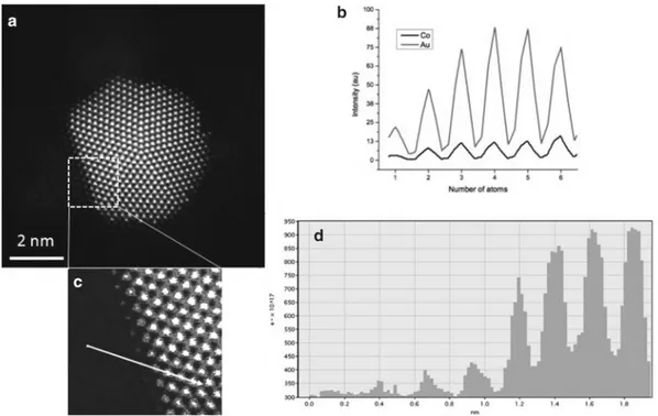
Fig. 16c is rotated 90° with respect to Fig. 16a . Figure 16a ¢ –c ¢ show respective simulated images. The difference in intensity between core and shell are evident. How can the Z-contrast capa-bilities of HAADF-STEM be used in the investigation of real metal nanoparticles? As an example, consider the Au-Co particle pre-sented in Fig. 17a . This particle was produced by the coalescence of a gold particle with a cobalt particle, both originally synthesized by inert gas condensation and deposited on a carbon substrate. After deposition, the system was subjected to a heating process. The particle in Fig. 17c shows an enlargement to remark the differences in intensity, as well as the intensity pro fi le in Fig. 17d . The two intensity pro fi les plotted in Fig. 17b show the simulated intensity pro fi les, described in Fig. 14 . This result exempli fi es the use of STEM simulations for an approximate description of com-position and shape of metal nanoparticles.
Using lower aperture of the condenser lens, spot number higher than 6, the beam current density incident in the sample would be less than 30 pA. Under these conditions and the alignment
7. Examples
of Stem-Imaging
of Metallic
Nanoparticles
469 37 Scanning Transmission Electron Microscopy Methods…
mentioned in the previous sections, the high resolution STEM is guaranteed. Decahedra gold nanoparticles can be identi fi ed at atomic scale in the Fig. 18 . Gold-palladium (Au/Pt) bimetallic Core-shell structures can be identi fi ed by differences in the con-trast in the HAADF-STEM imaging in Fig. 19 . The high contrast corresponds to the gold shell (Au with Z atomic weight 79) whereas the inner core showed lower contrast corresponding to a core of palladium (Pt with Z atomic weight 46).
The controlled incorporation of the metallic nanoparticles into biological systems is a challenge for the experimental scientist. The STEM imaging becomes as a critical tool to identify the incorpora-tion and the in fl uence of the multiple shapes into these biological
Fig. 18. Gold nanoparticles at atomic scale resolution. STEM image showing a few different gold nanoparticles ( a ); high magni fi cation of a decahedral nanoparticle ( b ) and theoretical model of this decahedral nanoparticle ( c ).
systems. Biologic systems contain mainly carbon, nitrogen, hydro-gen as the matrix. Therefore, the contrast in HAADF-STEM imag-ing is lower compared with the contrast generated by metallic nanoparticles. In this way, the identi fi cation of metallic nanostruc-tures embedded in biological tissue is relatively easy to observe. In the Fig. 20 silver nanoparticles are incorporated into bacteria and the particles can be clearly identi fi ed by contrast. HAADF-STEM imaging can avoid the staining procedure in comparison with the conventional TEM.
In summary, the scanning transmission electron microscope overcomes the barrier to atomic resolution, making it in one of the most powerful tools for characterization of nanomaterials. The new generation of aberration corrected microscopes, besides being a source of sophisticated characterization techniques, will certainly become a fundamental bridge between materials and health sci-ences. The capacity to control size, shape, and surface chemistry versatility of engineered nanoparticles has enabled their use into a plethora of biological and medical applications as drug delivery systems, therapeutics, diagnostics, and imaging contrast agents with different advanced functions and new properties. Depending of particular nanoparticle properties and mechanisms of interac-tion with biological systems, adsorpinterac-tion and uptake can produce dose-dependent decreases in cell viability and different metabolic and genetic alterations. These phenomena can be monitored with different well-established biochemical and molecular biology
471 37 Scanning Transmission Electron Microscopy Methods…
assays. The STEM methods mentioned in this chapter can be used to con fi rm attachment, internalization, and intracellular localiza-tion of these nanomaterials. As an example, cancer nanotechnology focuses on applications based on engineered nanoparticles designed for detection, diagnosis, targeting, and treatment of cancerous cells. Noble metal nanoparticles are biocompatible and non-toxic agents useful in all these biomedical applications at the cellular or molecular scale. Other important structural characteristics of nano-particles for biological and biomedical applications that need to be determined are: size, shape, hydrodynamic radius, zeta potential, surface charge, defects, chemical composition, and atomic struc-ture, that is highly related to functionality, stability, and reactivity of nanoparticles.
Acknowledgements
The authors would like to acknowledge THE WELCH FOUNDATION AGENCY PROJECT # AX-1615. “Controlling the Shape and Particles Using Wet Chemistry Methods and Its Application to Synthesis of Hollow Bimetallic Nanostructures.” The authors would also like to acknowledge the NSF PREM Grant # DMR 0934218, Title: Oxide and Metal Nanoparticles—The Interface between life sciences and physical sciences. The authors would also like to acknowledge RCMI Center for Interdisciplinary Health Research CIHR. “The project described was supported by Award Number 2G12RR013646-11 from the National Center for Research Resources. The content is solely the responsibility of the authors and does not necessarily represent the of fi cial views of the National Center for Research Resources of the National Institutes of Health.”
References
1. Pennycook S (1989) Z-contrast STEM for materials science. Ultramicroscopy 30:58–69 2. Ercolessi F, Andreoni W et al (1991) Melting
of small gold particles: mechanism and size effects. Phys Rev Lett 66:911–914
3. Ferrando R, Jellinek J et al (2008) Nanoalloys: from theory to applications of alloy clusters and nanoparticles. Chem Rev 108:845–910 4. Carter CB, Williams DB (2009) Transmission
electron microscopy: a textbook for materials science. Springer, New York
5. Fernández-Navarro C et al (2007) On the structure of Au/Pd bimetallic nanoparticles. J Phys Chem C 111:1256–1260
6. Kirkland EJ (1998) Advanced computing in electron microscopy. Springer, New York
7. Zuo JM, Olsen E (2011) http://cbed.matse. illinois.edu/JProbe/JProbe.html . Accessed 12 Aug 2011
8. Wall J, Langmore J, Isaacson M et al (1977) Scanning transmission electron microscopy at high resolution. Proc Natl Acad Sci 74:1802–1806
9. Ishizuka K (1998) Multislice implementation for inclined illumination and convergent-beam electron diffraction. In: Shiojiri M & Nishio K (eds) Proceedings of the International Symposium on Hybrid Analysis for Functional Nanostructure, Kyoto, Nakanishi Printing Co., pp 69–72