Electronic Structure of Quantum Dots:
Response to the Environment and
Externally Applied Fields
Author:
Carlos Segarra Ort´ı
Advisors:
Josep Planelles Fuster Juan Ignacio Climente Plasencia
June 2016
Departament de Qu´ımica F´ısica i Anal´ıtica Universitat Jaume I
CERTIFIQUEN:
Que la mem`oria presentada pel llicenciat Carlos Segarra Ort´ı amb t´ıtol
“Electronic Structure of Quantum Dots: Response to the Environment and
Externally Applied Fields” ha estat realitzada sota la nostra direcci´o i
cons-titueix la Tesi Doctoral de l’esmentat llicenciat. Autoritzem la presentaci´o
d’aquesta mitjan¸cant el present escrit.
Castell´o de la Plana, juny de 2016
Josep Planelles Fuster Juan Ignacio Climente Plasencia
La present Tesi doctoral ´es el resultat final de quatre anys de treball i esfor¸c en qu`e he tingut la sort de comptar amb el suport de companys, familiars i amics que han compartit amb mi aquesta enriquidora experi`encia. Sens dubte, el treball que ac´ı es mostra no haguera sigut possible sense la seua ajuda.
En primer lloc, voldria agrair a Josep Planelles i Juan Ignacio Climente el haver-me oferit la possibilitat de realitzar aquest projecte de Tesi sota la
seua supervisi´o. Durant tot el temps que he tingut el plaer de treballar amb
ells han mostrat un gran inter`es i una dedicaci´o plena en proporcionar-me
la millor formaci´o investigadora tenint sempre present el que seria millor
per al meu futur. De la mateixa manera, el meu agra¨ıment ´es extensiu a la
resta de membres del grup de Qu´ımica Qu`antica Fernando Rajadell, Jos´e
Luis Movilla, Miquel Royo i Ana Ballester que d’una manera o altra han
contribu¨ıt a la realitzaci´o d’aquesta Tesi. En especial vull destacar a Ana
B, amb qui vaig tindre la sort de compartir laboratori durant els primers anys de doctorat i que prompte es va convertir en una molt bona amiga.
D’altra banda, voldria mostrar tamb´e la meua gratitud als amics que han estat al meu costat en el dia a dia durant aquests anys i que han compartit amb mi molts bons moments dintre i fora de la universitat. En concret
vull destacar a Ana M, David, Erica, Neus, Paula i, com no, a ch´eritounet
Loucou. A m´es, cal mencionar a tots els membres del Departament de
Qu´ımica F´ısica i Anal´ıtica, especialment a Merche per la seva predisposici´o
a ajudar-me amb tota la paperassa i els tr`amits burocr`atics. Done tamb´e les
gr`acies a Sergio E. Ulloa per donar-me l’oportunitat de realitzar una estada
breu en el seu grup de recerca en la Universitat d’Ohio (Estats Units), aix´ı com a tots els membres del grup per la seua acollida.
Finalment, voldria agrair de cor als meus pares el suport i la confian¸ca
incondicionals que m’han donat durant tota la meua vida. Perqu`e s´on els
principals responsables de que haja arribat fins ac´ı, els dedique aquesta Tesi.
1D one-dimensional
2D two-dimensional
3D three-dimensional
AB Aharonov-Bohm
CB conduction band
ch crystal-field split hole
DQD double quantum dot
DSOI Dresselhaus SOI
e-h electron-hole
EFA envelope function approximation
EMA effective mass approximation
hh heavy-hole
LED light emitting diode
lh light-hole
PL photoluminescence
QD quantum dot
QR quantum ring
RSOI Rashba SOI
so split-off
TMDC transition metal dichalcogenide
VB valence band
WZ wurtzite
ZB zinc-blende
1 Introduction 1
2 Theoretical framework 9
2.1 The k·p method . . . 10
2.1.1 General formulation of the k·p method . . . 10
2.1.2 Envelope function approximation . . . 12
2.1.3 Hamiltonians for zinc-blende structures . . . 15
2.1.4 Hamiltonians for wurtzite structures . . . 17
2.1.5 Hamiltonians for polytypes . . . 19
2.2 Externally applied fields . . . 21
2.2.1 Electric field . . . 21
2.2.2 Magnetic field . . . 21
2.3 Spin-orbit interaction (SOI) . . . 23
2.3.1 Dresselhaus SOI . . . 24
2.3.2 Rashba SOI . . . 25
2.4 Strain and polarization fields . . . 25
2.4.1 Strain . . . 26
2.4.2 Piezoelectric polarization . . . 28
2.4.3 k·p Hamiltonians including strain and polarization fields 29 3 Magnetic field effects in semiconductor structures 31 3.1 Magnetic-field modulation of the hole ground state in cubic GaN/AlN QDs . . . 32
3.1.1 Effect of the aspect ratio . . . 34
3.1.2 Magnetic field modulation . . . 36
3.2 Aharonov-Bohm effect in systems with hexagonal symmetry . 37 3.2.1 AB effect in hexagonal quantum rings . . . 38
3.2.2 AB magnetoconductance oscillations and electron gas transitions in hexagonal core-shell nanowires . . . 43
4 Spin-orbit-induced spin relaxation in semiconductor QDs 53
4.2 Spin relaxation in 3D spheroidal QDs . . . 56
4.2.1 Electron spin relaxation . . . 57
4.2.2 Hole spin relaxation . . . 61
4.3 Electron spin-relaxation anisotropy in [001] and [111] grown QDs . . . 67
4.3.1 Effect of the QD geometry . . . 70
4.3.2 In-plane rotation of the QD . . . 72
4.3.3 [111] grown QDs . . . 74
4.4 Hole spin relaxation in InAs/GaAs quantum dot molecules . 75 4.5 Control of electron spin-orbit anisotropy in pyramidal QDs . 80 4.5.1 Angular dependence of the SOI . . . 82
4.5.2 Effect of the QD composition and height . . . 83
4.6 Summary . . . 84
5 Strain and piezoelectricity in wurtzite and polytype QDs 87 5.1 Piezoelectric control of exciton wave function in wurtzite QDs 88 5.1.1 Spheroidal dot-in-dot systems . . . 90
5.1.2 Other CdSe/CdS core-shell structures . . . 96
5.2 Spontaneous polarization in GaAs polytype QDs . . . 96
5.2.1 Electrons in GaAs WZ/ZB/WZ polytype QDs . . . . 100
5.2.2 Holes in GaAs ZB/WZ/ZB polytype QDs . . . 102
5.2.3 Excitons in GaAs WZ/ZB/WZ and ZB/WZ/ZB poly-type structures . . . 104
6 Edge states in monolayer MoS2 nanostructures 109 6.1 Effective Hamiltonian . . . 110
6.2 Results and discussion . . . 111
6.2.1 MoS2 nanoribbons . . . 111
6.2.2 MoS2 triangular QDs . . . 116
7 Conclusions 119 A Valence band Hamiltonians 123 A.1 Zinc-blende crystal structure . . . 123
A.1.1 Four-band Luttinger-Kohn Hamiltonian . . . 123
A.1.2 Six-band Burt-Foreman Hamiltonian . . . 124
A.1.3 Six-band Burt-Foreman Hamiltonian in cylindrical co-ordinates . . . 125
A.2 Wurtzite crystal structure . . . 129
A.3 Polytypes . . . 130
B Spin-orbit Hamiltonians in matrix form 133
B.1 Dresselhaus SOI . . . 133
B.1.1 Conduction band DSOI Hamiltonian . . . 133
B.1.2 Valence band DSOI Hamiltonian . . . 134
B.2 Rashba SOI . . . 135
B.2.1 Conduction band RSOI Hamiltonian . . . 135
C Strain Hamiltonians 137 C.1 Zinc-blende QDs . . . 137
C.1.1 Conduction band . . . 137
C.1.2 Valence band . . . 137
C.2 Wurtzite QDs . . . 138
C.2.1 Conduction band . . . 138
C.2.2 Valence band . . . 139
D Carrier-phonon interaction Hamiltonians 141 D.1 Piezoelectric potential . . . 142
D.2 Deformation potential . . . 143
D.2.1 Conduction band . . . 143
D.2.2 Valence band . . . 143
Resum 145
Publications 153
Bibliography 289
1
Introduction
Over the last decades, big efforts have been dedicated to the fabrication of smaller and smaller technological devices. This miniaturization process has led to structures with sizes in the nanometer scale (from few nanometers to few hundred nanometers). A clear example is the size evolution of the silicon transistors that integrate computer chips, decreasing from few micrometers to around 10 nm in the last 50 years. The investigation of such small systems has given rise to a relatively new area of research called nanotechnology, which is remarkably multidisciplinary and of current interest. When charge carriers (electrons and holes) are confined into systems with such length scale, of the order of their de Broglie wavelength, they start obeying the laws of quantum mechanics and a classical approach no longer holds. This fact is a natural limitation for the traditional methods of device fabrication, but it also offers fascinating novel physical properties that makes these structures promising candidates for future applications in medicine, electronics, solar cells and batteries, among others.[1]
In particular, nanoelectronic devices formed by low-dimensional semi-conductor nanostructures have been intensively investigated and various types of nanostructures have been developed. Based on the number of di-mensions in which the carriers are confined, these can be classified into quantum dots (QDs) (confined in all three spatial dimensions), quantum wires (confined in two dimensions) and quantum wells (confined in only one dimension). Each one of them presents different features, but this The-sis will mainly focus on the study of zero-dimensional QDs. As a result of the quantum confinement in these systems, their energy states form a discrete energy spectrum, similar to that of atoms. Due to this analogous
behavior, QDs are also known asartificial atoms.[2] However, both systems
present important differences. Electrons in an atom are subject to the at-tractive centrosymmetric Coulomb potential of the nuclei, while electrons in a QD move freely inside the available space defined by the confining potential. Additionally, the population of electrons inside a QD can be controlled from zero up to tens or even hundreds, and this is not possible working with atoms. This experimental tunability is an enormous advan-tage for QDs compared to atoms, since it offers the possibility to modify their electronic and optical properties through changes in size, shape and composition. For example, the color of the light emitted by CdSe QDs can be controlled by simply changing their size.[3] Bigger dots (radius of 5-6 nm) emit longer wavelengths like red, while smaller dots (radius of 2-3 nm) emit shorter wavelengths like green. This high tunability of properties is the reason why QDs are suitable for a wide range of applications such as pho-tovoltaic devices,[4] biosensors,[5] quantum computation,[6] light emitting diodes (LEDs),[7] lasers, display technologies,[8, 9] etc.
to fabricate QDs as colloidal semiconductor nanocrystals in glass dielectric matrices.[18] The first example of this method was carried out by Ekimov
et al. [19], who created CuCl microcrystals in a solution of silicate glass. Colloidal QDs are nearly spherical in shape with small radii in the range of 1.2-10 nm. Such QDs can be further covered by a layer of another semi-conductor material to form core-shell heterostructures that present altered properties in comparison to the uncovered ones. In light of the above, it is clear that the production method followed strongly determines the size and shape of the dots and, in turn, their properties. As for the materials used, typical dots are made of binary compounds of common zinc-blende (ZB) or wurtzite (WZ) semiconductors (PbS, PbSe, CdS, CdSe, InAs, GaAs, InP, GaN, InN and AlN) and their ternary and quaternary alloys. It is worth noting that QDs of some of these materials (e.g., GaAs and GaN) have been successfully synthesized in both crystal phases. Additionally, recent works have reported the fabrication of polytype QDs in which both ZB and WZ structures coexist within the same system.[20, 21] Moreover, since the discovery of graphene,[22] purely two-dimensional (2D) materials have been intensively studied and QDs made of graphene[23–25] and other related ma-terials such as monoloyer transition metal dichalcogenides (TMDCs)[26–28] have also been fabricated. As can be seen, the diversity of semiconductor QDs is very rich and it is still growing.
In order to use QDs in real devices, a good understanding of their prop-erties is needed from both experimental and theoretical points of view. As mentioned above, the optical and electronic properties of these structures are mainly governed by their shape, size and composition, i.e. by quantum confinement effects. Nevertheless, other factors that are intrinsic to the growth process, such as defects, impurities or crystal deformations to name a few, may also play an important role in their final performances. There-fore, it is crucial to identify and understand the phenomena that are relevant for each individual case under study, which will depend on the particular system and the application of interest. Then, based on this knowledge, QDs could be designed in order to enhance or diminish specific features. In addition to this, equally important is to have mechanisms to externally control and manipulate the system behavior in a reversible way. This is commonly done by switching on and off or changing the orientation of ex-ternal electric and magnetic fields. Consequently, the effects of these fields in the conduction band (CB) and valence band (VB) of QDs must be also studied.
subject to various relevant phenomena. Particularly, we focus on QDs of different shape, dimensions, and composition to explore their behavior un-der external fields and interactions with the environment. Typical QDs are embedded into or grown on top of a different material, so that the lattice mismatch at the interface originates strain and this strain, in turn, gives rise to piezoelectricity. Here, the influence of these effects on the CB and VB electronic structure is explored, paying special attention to the role of the crystal phase, namely ZB, WZ or polytype crystal structure. Fur-thermore, the relaxation of the spin degree of freedom confined in QDs is also studied. Such spin scattering is mediated by the coupling of the spin states with acoustic phonons of the surrounding medium via the deforma-tion and the piezoelectric potential mechanisms. For the relaxadeforma-tion to take place, the states involved in the transition need some spin admixture, which is produced by the spin-orbit interaction (SOI) in our case. By including all relevant sources of spin mixing (Rashba SOI (RSOI), Dresselhaus SOI (DSOI), and the coupling of light-hole (lh) and heavy-hole (hh) subbands) in a fully 3D model, it is shown that SOI is strongly anisotropic, which also translates into anisotropic spin relaxation. Additionally, the behavior of electrons and holes under externally applied fields is also investigated, focusing on the possibility of inducing ground state transitions and the emergence of the Aharonov-Bohm (AB) effect in quantum rings (QRs) as a consequence of their doubly-connected topology. Another topology-related
effect is also analyzed in monolayer MoS2, a truly 2D system in which edge
states are formed owing to the marginal topological character of the MoS2
material.
In the succeeding chapters we present the theoretical methods and the main findings of this Ph.D. Thesis together with a reasoned interpretation of the results. The remainder of this dissertation is structured as follows:
In chapter 2 we introduce the theoretical formalism used to model the electronic structure of the CB and the VB of semiconductor
nanostruc-tures.1 To be specific, the description of electrons and holes in such systems
is carried out by means of the k·p method within the effective mass
approx-imation (EMA) and the envelope function approxapprox-imation (EFA). Briefly, it consists in a semi-empirical continuum model based on perturbation theory that provides good estimates of the low-energy properties at a relatively low computational cost. The Hamiltonians employed to investigate struc-tures made of ZB, WZ, and mixed crystal phases (polytypes) are presented.
Besides being computationally low demanding, k·p methods are also
vantageous because they allow to take into account many phenomena by simply supplementing the base Hamiltonians with appropriate extra terms. In this respect, the basic aspects and the explicit Hamiltonians describing such phenomena are exposed, namely external electric and magnetic fields, SOI, strain, and piezoelectricity. For the latter two, the corresponding fields are calculated using the continuum theory of elasticity.
Chapter 3 is dedicated to study the effects of applying an external mag-netic field in two different systems. First, the electronic structure of the VB in axially-symmetric GaN/AlN cubic QDs is investigated. A position-dependent six-band Hamiltonian in cylindrical coordinates is derived to ex-plore the hole spin purity and the possibility of modulating the energy spectrum via magnetic fields to cause inversions of the ground state. In this way, optical properties such as light polarization could be easily tuned. Second, the response of nanostructures in the multi-particle regime pierced by axial magnetic fields is analyzed. In particular, the system considered is a flat hexagonal QR defined as the cross-section of a multishell nanowire. Remarkable signatures of the discrete geometry symmetry and of the cor-relation are found in the AB oscillation patterns, which allow to justify observations reported in recent magnetoconductance experiments.
In chapter 4 we describe the physics of the spin of carriers confined in zero-dimensional structures with various shapes, dimensions and crystallo-graphic orientations. Special attention is paid to the SOI and its role in the spin relaxation of electrons and holes. Both RSOI and DSOI effects are taken into account in a fully 3D model, going beyond the commonly employed quasi-2D simplified description in which cubic DSOI terms are disregarded. Indeed, the importance of including all three spatial dimen-sions is confirmed in self-assembled dots and core-shell nanocrystals which are clearly not flat. Also, the high anisotropic character of the spin relax-ation is shown by varying the aspect ratio of the QDs and by rotating the orientation of external magnetic fields. Such anisotropy leads to substan-tial spin relaxation suppressions, offering the possibility to obtain long-lived spins. Furthermore, for the VB the geometry regime at which the different sources of spin mixing, i.e. SOI or lh-hh coupling, prevail is identified. In addition, the intrinsic anisotropy of RSOI and DSOI is also demonstrated by studying the magnitude of the spin anticrossings in the energy spectra. All results are discussed in terms of the symmetry of the SOI Hamiltonians.
undesirable for some applications, they offer the opportunity to fabricate strain-engineered QDs with improved performance.[29, 30] Two systems with different crystal structure are considered, core-shell WZ nanocrystals and polytype QDs, in order to assess the role of the crystal phase in these phenomena. It is known that the generated piezoelectric fields are usually weak in ZB structures, but they turn out to be crucial in WZ and even more in polytype systems, where spontaneous polarization is found to predomi-nate. It is shown that the resulting polarization fields strongly affect the electron-hole (e-h) spatial separation, thus enabling a substantial exciton lifetime tunability.
Lastly, in chapter 6 we investigate atomically thin structures. In
par-ticular, the electronic structure of monolayer MoS2 nanoribbons and QDs
is analyzed. In such systems, states spatially localized near the edges and with energies lying in the band gap emerge, which play an important role in transport properties. The origin of these edge states is related to the marginal topological character of the system Hamiltonian.
The contents of the present report are based on the publications in which the author has contributed during the last four years. All of them have been published in international peer-reviewed journals. A copy of the works listed below can be found at the end of the present doctoral Thesis.
1. C. Segarra, J. I. Climente, and J. Planelles, Valence band mixing of
cubic GaN/AlN quantum dots, J. Phys.: Condens. Matter 24, 115801 (2012)
2. J. Planelles, J. I. Climente, and C. Segarra,Electron spin relaxation in
3D quantum dots: geometrical suppression of Dresselhaus and Rashba spin-orbit interaction, J. Phys. Chem. C116, 25143 (2012)
3. J. I. Climente, C. Segarra, and J. Planelles, Spin-orbit-induced hole
spin relaxation in InAs and GaAs quantum dots, New J. Phys. 15, 093009 (2013)
4. A. Ballester, C. Segarra, A. Bertoni, and J. Planelles, Suppression
of the Aharonov-Bohm effect in hexagonal quantum rings, EPL 104, 67004 (2013)
5. M. Royo, C. Segarra, A. Bertoni, G. Goldoni, and J. Planelles,
Aharonov-Bohm oscillations and electron gas transitions in hexagonal core-shell nanowires with an axial magnetic field, Phys. Rev. B 91, 115440 (2015)
6. C. Segarra, J. Planelles, and J. I. Climente, Control of electron
spin-orbit anisotropy in pyramidal InAs quantum dots, Physica E 66, 234 (2015)
of spin-orbit induced electron spin relaxation in [001] and [111] grown GaAs quantum dots, New J. Phys. 17, 033014 (2015)
8. C. Segarra, J. I. Climente, F. Rajadell, and J. Planelles, Hole spin
relaxation in InAs/GaAs quantum dot molecules, J. Phys.: Condens.
Matter27, 415301 (2015)
9. C. Segarra, J. Planelles, and S. E. Ulloa,Edge states in dichalcogenide
nanoribbons and triangular quantum dots, Phys. Rev. B 93, 085312 (2016)
10. J. I. Climente, C. Segarra, F. Rajadell, and J. Planelles, Electrons,
holes, and excitons in GaAs polytype quantum dots, J. Appl. Phys.
119, 125705 (2016)
11. C. Segarra, J. I. Climente, A. Polovitsyn, F. Rajadell, I. Moreels,
and J. Planelles, Piezoelectric control of the exciton wave function
2
Theoretical framework
The aim of this chapter is to provide the theoretical background of the methods used throughout this Thesis for the calculation of the QD elec-tronic structure. A brief discussion of the general aspects of the methods is presented here and whoever interested in further details is invited to consult dedicated books.[31–33] Nevertheless, when extra information is required for understanding a specific topic, this will be given in the corresponding chapter.
The models typically employed to study QDs can be classified into two categories: atomistic and continuum models. Atomistic models, e.g. empiri-cal pseudopotential and tight-binding methods, take all atoms of the crystal and their interactions explicitly into account in order to describe the behav-ior of the system. These models are generally considered more accurate because they are based on more fundamental principles, but have the dis-advantage of being computationally expensive (typical QDs are composed
by 103-106 atoms) and the results are often hard to interpret. On the other
hand, continuum models treat the systems as an ensemble of material do-mains whose properties are those of the bulk, thus ignoring the microscopic details. Although less accurate, these simpler models yield good estimates of the low-energy properties, offering more intuitive and computationally less demanding results.
Particularly, the approach taken for this Ph.D. project is the k·p method
in the framework of the EMA and EFA. In spite of its simplicity, this con-tinuum model has been successfully used to capture the main electronic and optical features of QDs at a reasonable computational cost. Additionally, it allows the implementation of phenomena such as externally applied fields or strain in a straightforward way.
2.1
The k
·
p method
The k·p method was originally developed in the 1950s for the calculation
of the band structure of bulk semiconductors and adapted to study het-erostructures subsequently. It is a perturbative method that takes advan-tage of the crystal symmetries to predict the band structure as a function of only a few empirical parameters, which are obtained from experiments orab initio calculations.
2.1.1 General formulation of the k·p method
An electron moving in a crystal, i.e. in the periodic potential of the atomic
nuclei, is governed by the following Schr¨odinger equation including
spin-orbit:
p2
2m0
+ ~
4m2 0c2
p· σ×∇Vcr(r)
+Vcr(r)
ψ(r) =E ψ(r), (2.1) whereVcr(r) =Vcr(r+R) is the periodic potential,p=−i~∇,m0is the free
electron mass,cis the velocity of light in vacuum andσstands for the vector
of Pauli spin matrices.1 Taking into account Bloch’s theorem, the wave
function of a particle in a periodic potential can be written as the product
of a plane wave, eikr, and a periodic function with the same periodicity as
the potential, unk(r) =unk(r+R). After substituting ψnk(r) =eikrunk(r)
into (2.1) and left multiplying by e−ikr one obtains
p2
2m0
+ ~
2k2
2m0
+ ~
4m2 0c2
p·(σ×∇Vcr) + ~
m0
k·π+Vcr
unk =Enkunk
(2.2) with
π=p+ ~
4m20c2(σ×∇Vcr). (2.3)
The second term of π, coming from the spin-orbit effect, has a small
con-tribution and will be disregarded hereafter, so that π=p.
Equation (2.2) is the basic formulation of the k·p method, whose name
comes from the appearance of the k·p factor2. It can be solved for a fixed
wave vector k=k0, yielding a complete and orthonormal set of
eigenfunc-tions unk0. For simplicity, k= 0 is usually taken at the band extrema (the
1 The components ofσ areσ
x= (0 11 0), σy= 0i−0i, andσz= 1 00−1
.
Γ point in common semiconductors). Then, the band dispersion at finite
k can be calculated by means of perturbation theory. To this end,
equa-tion (2.2) is rewritten as the sum of the Hamiltonian for k = 0, H0, plus
the k-dependent terms as a perturbation,Hk0.
p2
2m0
+ ~
4m20c2p·(σ×∇Vcr) +Vcr
| {z }
H0
+~
2k2
2m0
+ ~
m0
k·p
| {z }
Hk0
unk =Enkunk
(2.4)
In practice, only a limited number of functions can be taken as basis set. As a result, the validity of the results is restricted to a small area in the vicinity of the Brillouin zone center. Nevertheless, the physics of semiconductors is mostly governed by the carriers in the extrema of the
various energy bands and, thus, the k·p method suffices to capture their
main properties.
The choice of the bands included in the model depends on how isolated the bands of interest are. Let us consider a situation where the investigated
band is far from the other bands. In such a case,unkis mainly determined by
un0and a basis set consisting of only this function can be used. This is true,
as will become clear below, for the CB of most semiconductors. Applying second order non-degenerate perturbation theory to (2.4), the expressions
forEnk and unk are obtained
Enk =En0+~ 2k2
2m0
+ ~
2
m2 0
X
n06=n
|hun0|k·p|un00i|2
En0−En00 (2.5)
and
unk =un0+ ~ m0
X
n06=n
hun0|k·p|un00i En0−En00
un00. (2.6)
Here,En0 and the so-called optical matrix elementsPnn0 =hun0|k·p|un00i are unknown parameters that need to be inferred from experiments. Equa-tion (2.5) can be rewritten as
Enk =En0+~ 2k2
2m∗ (2.7)
where m∗ is known as the effective mass of the band. This modified mass
arises from the coupling of the considered band with other neighboring
bands via thek·p term and has the following form:
1
m∗ =
1
m0
+ 2
m20k2
X
n06=n
|hun0|k·p|un00i|2 En0−En00
The values of the effective masses are deduced from experimental data and are tabulated for most materials. A comparison between equation (2.7) and the Hamiltonian of a free electron show that both expressions are identical except for the mass. Then, the motion of an electron in a crystal can be seen as the motion of a free electron whose mass has been modified by the action of the periodic potential. This one-band model showing a quadratic dispersion relation is also known as EMA and, despite its simplicity, it has been extensively used in literature with surprisingly good results in the description of the CB.
Contrary to the previous example, when studying the VB the bands of interest are commonly close in energy to other bands and they cannot be treated independently. In such a case, multiband models are necessary and
the quasi-degenerate perturbation theory proposed by L¨owdin [34] should be
used. Thek·pinteraction between the few adjacent bands is explicitly taken
into account, while the contribution from remote bands is introduced using
the L¨owdin perturbation theory. This approach results in a N-dimensional
Hamiltonian containing additional terms of higher order in k, with N being
the number of bands included.
The separation between bands strongly depends on the material and its crystal structure. So, the model employed has to be selected based on the characteristics of the system under investigation. In sections 2.1.3 and 2.1.4 some typical cases will be discussed for ZB and WZ semiconductors. In general, single-band models for the CB and four- or six-band models for the VB are enough to obtain satisfactory results for most low-energy properties.
2.1.2 Envelope function approximation
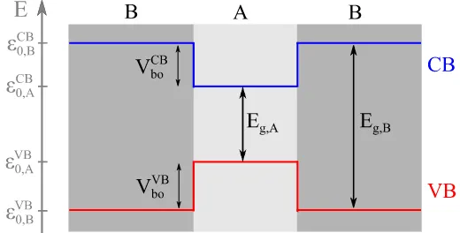
The development of epitaxial growth techniques in the 1970s led to the fabrication of the first heterostructures with atomically sharp interfaces. In such systems, the carriers are confined due to the band misalignment of the constituting materials, as represented in figure 2.1.
The breaking of the translational invariance at the interface prevents the
use of the k·p model in these nanostructures. Several alternative theories
Figure 2.1: Sketch of the band edge profile along the z direction in a direct-gap heterostructure formed by two materials A and B. Band-edge energies (εCB
0,A,εCB0,B,εV B0,A andεV B0,B), band gaps (Eg,A andEg,B) and band offsets (VboCB andVboV B) are indicated for both CB and VB.
the periodic parts of the Bloch functions to be the same in both materials,
uA
nk =uBnk =unk. Then, the wave function can be expanded as
ψnk(r) =
X
n
fn(A,B)(r)unk0(r), (2.9)
where fn(A,B)(r) is fnA(r) or fnB(r) depending on the region. This function
varies slowly at the scale of the unit cell and it is usually referred to as envelope function.
For simplicity, a basis consisting of one band is used hereafter. Similarly
to the derivation of the k·p method in the preceding section, equation (2.9)
can be substituted into the Schr¨odinger equation (2.1) without spin-orbit
and, after some algebraic manipulation3, one gets
− ~ 2
2m0
∇2+ε0,A+Vbo(r)
fn(A,B)(r) =E fn(A,B)(r). (2.10) Here,ε0,A is the band energy of material A atk= 0 andVbo(r) is a step-like
function that takesVbo(r∈A) = 0 in layer A andVbo(r∈B) =Vbo(CB,V B)in
layer B. Equation (2.10) is the second-order differential equation that gov-erns the spatial behavior of the envelope function. This equation is solved after taking into account the appropriate boundary conditions. Typically,
infinite barriers (V =∞) at the outer edges and the continuity of the wave
function derivative at the interface are imposed.
Just as the k·p method, this model can be further improved by pertur-batively including the interaction with remote bands through the effective mass and by using several bands as basis in a multiband model. A com-parison between both methods shows that the EFA Hamiltonian can be
obtained from the k·p one by setting~k→ −i~∇and adding a few terms.
Hence, both models depend on the same set of parameters Pnn0.
Conse-quently, due to the close similarity, EFA Hamiltonians are also known as
k·p-EFA models.
The-one band model presented above is the simplest description of a heterostructure in which the presence of two materials is only taken into account through the band offset. Nevertheless, in such systems the effective
massm∗and the other band parameters become position dependent, so that
kandm∗do not commute. This fact complicates the choice of the boundary
condition at the interface. In fact, there has been much debate on the topic
and several effective mass matching conditions have been proposed.4
The simplest model is the one based on BenDaniel-Duke boundary condi-tion.[36] It considers a single parabolic and isotropic band and obtains a new Hamiltonian by changing the order of the differential operators in (2.10):
− ~ 2
2m∗∇2 is replaced by −
~2
2 ∇
1
m∗(r)∇. (2.11)
The new symmetrized Hamiltonian ensures the hermiticity and, thus, so-lutions with real eigenvalues and orthogonal eigenfunctions. The boundary condition is the continuity of fn(r) and m∗1(r)dfdrn at the interface. It is in-teresting to notice that the effective mass mismatch leads to a discontinuity in the derivative of the envelope function at the interface.
Similarly, the operator symmetrization approach has also been widely used in the description of holes in heterostructures. In such a case, a generic matrix element of a VB multiband model
H=X
ij
Hij(2)kikj+
X
i
Hi(1)ki+H
(0) (2.12)
is rewritten for a variable mass system as
H=X
ij
kiHij(2)kj+
X
i
(Hi(1)ki+kiH(1)i ) +H(0). (2.13)
This reordering of the operators is, however, not strictly correct and may produce unrealistic results in some cases. As a consequence, in this Thesis
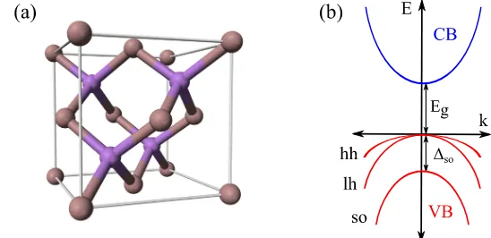
Figure 2.2: (a) Unit cell of ZB GaAs. Arsenic atoms are depicted in gray and gallium atoms in purple. (b) Schematic band dispersion of a ZB structure. The principal bands and their energy separations at the Γ point are indicated. For finitekthe valence band is split in three subbands: hh, lh and split-off (so).
we follow the so-called Burt-Foreman model. Burt followed a completely different approach compared to Bastard’s formalism. Instead of proposing an heuristic Hamiltonian and then search for valid solutions, he derived an exact envelope function theory from first-principles by first establishing con-straints to the envelope function.[37–39] Later, Foreman used Burt’s theory to derive an explicit multiband Hamiltonian and showed that this model gives reasonable results in particular cases where a symmetrized version
of a conventional k·p model, namely the Luttinger-Kohn model, leads to
nonphysical solutions.[40, 41]
2.1.3 Hamiltonians for zinc-blende structures
ZB is, together with WZ, one of the most common crystal structures in which binary semiconductors are grown. Examples are GaAs, InAs, CdTe and AlSb, to name a few. The crystal lattice consists of a face-centered cubic array of anions with cations occupying one half of the tetrahedral holes as figure 2.2(a) illustrates. This structure lacks inversion symmetry and corresponds to one of the piezoelectric crystal classes. Piezoelectric effects in QDs will be discussed in section 2.4.2.
On one hand, the band gap Eg of the semiconductors studied in this
Thesis is relatively large and allows the theoretical description of the CB in terms of a single-band model. The Hamiltonian reads
H =−~
2
2∇
1
m∗(r)∇+V(r) (2.14)
where a position-dependent effective massm∗(r) is assumed andV(r) stands
for the confining potential.
On the other hand, a multiband model is necessary to study the top of the VB. In the absence of spin-orbit the three valence subbands are
degenerate, but spin-orbit lifts this degeneracy even fork= 0. As shown in
Fig. 2.2(b), the so subband becomes separated from the other two by the
spin-orbit splitting ∆so. Then, depending on the magnitude of ∆so, a
four-or six-band model should be employed.
From a microscopic point of view, the electronic bands are formed due to the hybridization of the valence s- and p-orbitals. In fact, the CB and the VB are mainly made of s- and p-orbitals, respectively. Thus, the most
simple set of unperturbed basis functions are the Bloch functions: |S↑i,
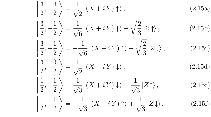
|X ↑i, |Y ↑i, |Z ↑i, |S ↓i, |X ↓i, |Y ↓i and |Z ↓i. However, it is more convenient to use a basis set made of a linear combination of the above functions that is adapted to the total angular momentum. This new basis set is5
3 2,+
3 2
= √1
2|(X+i Y)↑i, (2.15a)
32,+12
= √1
6|(X+i Y)↓i −
r
2
3|Z↑i, (2.15b)
3 2,−
1 2
=−√1
6|(X−i Y)↑i −
r
2
3|Z↓i, (2.15c)
32,−32
= √1
2|(X−i Y)↓i, (2.15d)
12,+12
= √1
3|(X+i Y)↓i+ 1
√
3|Z↑i, (2.15e)
1 2,−
1 2
=−√1
3|(X−i Y)↑i+ 1
√
3|Z↓i. (2.15f)
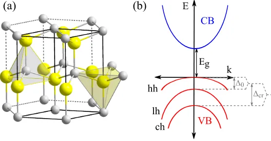
[image:30.595.120.463.487.678.2]Figure 2.3: (a) Hexagonal structure of a WZ crystal, e.g. GaN. Gallium atoms are depicted in gray and nitrogen atoms in yellow. (b) Drawing of the band dispersion of a typical WZ semiconductor with ∆cr > ∆0. Band gap Eg, crystal-field splitting ∆cr and spin-orbit splitting ∆0 are indicated.
In this basis, the total angular momentum and it’s projection Jz become
diagonal in matrix representation.
Throughout the present dissertation, various multiband models are used to investigate the valence band of QDs. The choice of a particular method
is based on the material, specifically the value of ∆so, and the particular
type of QD studied. In appendix A, all Hamiltonians used are collected together for ease of reference. The four-band Luttinger-Kohn Hamiltonian for constant mass calculations is given in appendix section A.1, and the six-band variable-mass Burt-Foreman one in section A.2.
2.1.4 Hamiltonians for wurtzite structures
WZ is the other typical crystal structure for binary semiconductors. Among the compounds that can take the WZ structure are CdS, CdSe, GaN, AlN, etc. It is constructed from two interpenetrating hexagonal-close-packed lat-tices, as represented in figure 2.3(a). WZ and ZB crystals are quite similar since their structure differ only in the second-nearest neighbors. Neverthe-less, this difference causes WZ to have lower symmetry and this, in turn, results in two additional features compared to ZB materials: the emergence
of the crystal-field splitting ∆cr and spontaneous polarization
Figure 2.3(b) displays the band structure of a common WZ semiconduc-tor. Similarly to ZB, four spinless bands are taken into account to study the properties of WZ QDs. However, this selection is not as clear as for ZB because the separation of the CB lowest in energy from other conduction bands is rather small for some WZ materials.[42] In spite of this, a single-band parabolic Hamiltonian is used in the present Thesis due to the lack of effective mass parameters describing such a coupling.
With respect to the VB, it can be seen that, unlike ZB, the three (spin
doubly degenerate) valence bands are split at k = 0. In the absence of
spin-orbit coupling, the hexagonal crystal field (∆cr) splits the p-like bands
into two degenerate subbands and the crystal-field split hole (ch) subband.
With the inclusion of spin-orbit coupling (∆0), the degenerate subband is
further split into the hh and the lh subbands. In some works, the hh, lh and ch subbands are also referred to as A, B and C subbands, respectively. It is interesting to notice that the order of the lh and ch shown in figure 2.3(b)
can be altered depending on the values of ∆cr and ∆0. Because of this, a
six-band model is commonly used in WZ simulations.
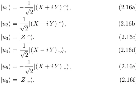
Contrary to ZB, the lower symmetry of WZ does not allow to find a
basis set that diagonalizes the Hamiltonian at k = 0. The basis of Bloch
functions considered here is[43]
|u1i=− 1
√
2|(X+i Y)↑i, (2.16a)
|u2i= 1
√
2|(X−i Y)↑i, (2.16b)
|u3i=|Z ↑i, (2.16c)
|u4i= 1
√
2|(X−i Y)↓i, (2.16d)
|u5i=− 1
√
2|(X+i Y)↓i, (2.16e)
|u6i=|Z ↓i. (2.16f)
Various authors have reported six-band models to study the WZ VB.[32, 43, 44] In this Thesis, a position-dependent Hamiltonian derived following Burt-Foreman operator ordering is used.[45] The matrix representation can be found in appendix A.2. This Hamiltonian depends on 6 mass parameters
A1−6 and three energy splittings ∆1−3, with ∆1 = ∆cr, and ∆2 and ∆3
being the spin-orbit matrix elements (∆2 = ∆3 = ∆so/3 in the so-called
[image:32.595.221.459.451.601.2]Figure 2.4: Crystal structures and their stacking sequence for (left) ZB in the [111] direction and (right) WZ in the [0001] direction. Reprinted with permission from [46]. Copyright 2012, AIP Publishing LLC.
2.1.5 Hamiltonians for polytypes
As mentioned above, WZ and ZB crystals present close similarities. This becomes evident when considering the ZB structure in the [111] direction and comparing it to WZ [0001]. In figure 2.4, it can be seen that both structures only differ in the stacking order of the layers: ABCABC for ZB while ABABAB for WZ. As a result, polytypical nanostructures consisting of ZB [111] and WZ [0001] phases of the same material have been suc-cessfully fabricated.[20, 21] These systems present typical characteristics of heterostructures formed by different materials because the band gap and the parameters also depend on the crystalline phase.
The theoretical study of these systems requires a model able to describe both crystal structures simultaneously. For the CB, this can be done by simply considering a different effective mass for each region in a position-dependent one-band Hamiltonian. For the VB, instead, this may seem a complicate task in view of the six-band Hamiltonians proposed for both structures in appendix A. However, Bir and Pikus realized in their book (see page 328 in [32]) that a transformation of the ZB Hamiltonian to the
appropriate coordinate system6 yields a new Hamiltonian which is similar
6 In the new coordinate system, thez0-axis is along [111] direction andx0- andy0-axis
to the WZ one. This opens the possibility of constructing a general Hamil-tonian for the whole system and then particularize it to the structure of each region by considering the pertinent parameters.
In order to compare both Hamiltonians systematically the Bloch basis functions of lower symmetry should be used, i.e. the basis set of WZ given in 2.16. In this basis, one gets a Hamiltonian for ZB that is formally identical to the standard WZ one, equation (A.4), but now two extra terms emerge:
∆K= 2√2 ~
2
2m0
Azk−kz, (2.17a)
∆H= ~
2
2m0
Azk2−. (2.17b)
These terms are zero for WZ (Az = 0) and allow the ZB Hamiltonian
to regain the original isotropic symmetry. In addition to this, the following relations arise connecting the mass parameters and energy splittings of both structures:
∆1 = 0, (2.18a)
∆2 = ∆3= ∆so/3, (2.18b)
A1 =−γ1−4γ3, (2.18c)
A2 =−γ1+ 2γ3, (2.18d)
A3 = 6γ3, (2.18e)
A4 =−3γ3, (2.18f)
A5 =−γ2−2γ3, (2.18g)
A6 =− √
2(2γ2+γ3), (2.18h)
Az =γ2−γ3. (2.18i)
Taking into account (2.18) reduces the number of independent parameters from 9 in WZ to 4 in ZB, as expected from symmetry considerations.
The full six-band Hamiltonian derived to study polytypes can be con-sulted in appendix A.3.1. It is worth noting that all diagonal elements are
over stabilized by ∆so/3 when using ZB parameters. Thus, equation (A.3.1)
must be corrected by subtracting this amount in the ZB region.
following the same procedure as before, a position-dependent Hamiltonian for polytype systems is constructed. See appendix A.3.2 to consult its full matrix form. As expected from Foreman [40], the resulting Hamiltonian presents some extra coefficients compared to (A.5).
2.2
Externally applied fields
Particle energy levels are modified in the presence of external fields. This paves the way for manipulating the properties of QDs and, thus, controlling devices by external means.
2.2.1 Electric field
An external homogeneous electric field pulls electrons and holes towards op-posite directions, leading to lower e-h overlaps and the suppression of exciton recombination processes. In addition, it is also responsible for the quantum-confined Stark effect, which generates a redshift of the emitted/absorbed light.
Accounting for static electric fields Finto k·p Hamiltonians is
straight-forward. An extra potential energy VF needs to be added to the confining
potential of the heterostructure
VF (r) =−eF·r (2.19)
whereeis the particle charge, e=−1 for electrons and e= 1 for holes.
It is worth stressing that the presence of electric fields may also give rise to other phenomena in nanostructures, e.g. the Rashba SOI (see sec-tion 2.3.2).
2.2.2 Magnetic field
The application of magnetic fields to QDs originates shifts in the energy spectrum and lifts of spin degeneracies. The latter phenomenon is known as Zeeman effect and is the magnetic field analogous of the Stark effect.
The standard way of including a magnetic field B in the k·p-EFA
for-malism is via minimal coupling, i.e. by replacing the canonical momentum
Hamiltonian. Here, e is the particle charge and A is the vector potential
defining the magnetic field B=∇×A. The choice of the vector potential
is not unique and it is common practice to use a different version based on the symmetry of the problem.
In a one-band isotropic model describing the CB and with position-dependent effective mass, the resulting Hamiltonian is as follows:
H= 1
2(−i~∇−eA) 1
m∗(r)(−i~∇−eA) +V (r) + g∗
2µBσ·B (2.20)
The last term in (2.20) is the Zeeman splitting, where g∗ is the effective
Land´e g-factor, µB = 2|em|~0 the Bohr magneton and σ is a vector whose
components are the Pauli matrices.
As for the magnetic field implementation in multiband models, the mini-mal coupling approach first used by Luttinger [48] has been widely employed in literature, providing satisfactory results for many experimental evidences. However, this model has been unable to describe some particular observa-tions, such as the photoluminescence (PL) magnetoresonances in QRs under axial magnetic fields.[49] In this regard, recent works have proposed a new approach which outperforms the Luttinger approximation.[50, 51] It consists
in performing the same replacement,p→ −i~∇−eA, but now prior to
ap-plying the EFA. The Hamiltonian obtained, unlike the Luttinger model, has
no off-diagonal terms depending on B, thus reducing the coupling between
hole subbands.
We particularize this approach for a ZB constant mass system under
an axial magnetic field B = (0,0, B0) defined by the vector potential A=
B0
2 (−y, x,0). In this specific case, the six-band Hamiltonian supplementing the zero-field one (A.2), presents the following diagonal elements:
H11B =−(γ1+γ2)
B02(x2+y2)
8 +
B0
2 (xpy −ypx)
−3
2κ µBB0 (2.21a)
H22B =−(γ1−γ2)
B02(x2+y2)
8 +
B0
2 (xpy −ypx)
−1
2κ µBB0 (2.21b)
H33B =−(γ1−γ2)
B02(x2+y2)
8 +
B0
2 (xpy −ypx)
+1
2κ µBB0 (2.21c)
HB
44=−(γ1+γ2)
B2
0(x2+y2)
8 +
B0
2 (xpy −ypx)
+3
2κ µBB0 (2.21d)
H55B =−γ1
B02(x2+y2)
8 +
B0
2 (xpy−ypx)
−1
2κ
0µ
H66B =−γ1
B2
0(x2+y2)
8 +
B0
2 (xpy−ypx)
+1
2κ
0µ
BB0 (2.21f)
withκ and κ0 standing for the hole effective g-factors andµB= 2|em|~0.
As can be seen in (2.20) and (2.21), the Zeeman energy splitting is mainly determined by the value of the effective g-factor. In bulk systems,
the SOI causes the g-factor to deviate from the bare electron value g ≈2
and effective g-factors g∗ are inferred experimentally. In QD simulations
it is common to use these bulk effective g-factors, although some works have pointed out the quenching of the SOI-induced deviation in QDs due
to confinement.[52] In this respect, van Breeet al.[53] suggest to disregard
the contribution from remote bands and simply consider the bare Land´e g-factors: g∗= 2, κ= 4/3 and κ0 = 2/3.
2.3
Spin-orbit interaction (SOI)
In this section, we will present a theoretical description of the SOI effects on the CB and the VB of ZB materials. The SOI in WZ semiconductors is omitted here since in the present Thesis the spin dynamics of these crystal structures is not investigated.
In atomic physics, the SOI is a well-known phenomenon originating from the coupling of the electron spin to its orbital momentum via the electric field generated by the nuclei. Similarly, the SOI in solids comes from the in-teraction between the spin and the average electric field of the lattice nuclei. The most relevant effect of SOI on the band structure of semiconductors is the degeneracy breaking of the three topmost VB subbands. In particu-lar, in cubic semiconductors such as ZB or diamond crystal structures this causes the energy separation at the center of the Brillouin zone of the so band from the lh and hh ones, which remain degenerate. In addition to this, SOI is also responsible for the spin splitting of the bands in materials lacking inversion symmetry, e.g. ZB semiconductors, even in the absence of a magnetic field. As a result, the CB and the three VB are no longer doubly spin-degenerate. The latter effect is, however, relatively small and it does not significantly affect most electronic properties, thus justifying not including it in many studies. Nonetheless, it may play an important role when investigating the properties of the spin degree of freedom,[54–56] such as the spin dynamics we will deal with in chapter 4.
The models discussed in the previous sections take into account the
ignore the spin-orbit-induced spin splitting. In order to include this effect, the Hamiltonians need to be supplemented by extra terms coming from the SOI contribution in equation (2.3) that was initially disregarded. The expressions of these additional terms can be obtained by using both the theory of invariants or perturbation theory up to third or fourth order. For the sake of brevity, their derivation will not be presented here, but we invite the interested reader to consult Winkler’s book [33] for a detailed presentation.
Next, we will briefly discuss the origin and introduce the Hamiltonians of the two main spin-orbit sources of spin splitting in ZB materials: DSOI and RSOI.
2.3.1 Dresselhaus SOI
The DSOI is an intrinsic property of some materials resulting from the absence of an inversion center in its crystal structure.[57] In such a case, the microscopic electric fields generated by the lattice atoms do not cancel each other, thus originating a net contribution to the SOI. This phenomenon is also known as bulk inversion asymmetry (BIA).
For the CB, there are no terms up to second order in k, so that the
cubic contributions are the lowest-order terms that characterize DSOI. The corresponding Hamiltonian for electrons reads:[33]
HCB
BIA =bCB41
σxkx k2z−ky2
+σyky k2x−kz2
+σzkz ky2−kx2
, (2.22)
where bCB
41 is a material-dependent parameter.
On the other hand, the contribution of DSOI in the VB includes
linear-and third-order-in-kterms and is given by:[33]
HBIAV B = √2
3Ck
kx{Jx, Jy2−Jz2}+ cp
+bV B
41
{kx, k2y−k2z}Jx+ cp
+b42 {kx, ky2−kz2}Jx3+ cp
(2.23) +b51
{kx, ky2+kz2} {Jx, Jy2−Jz2}+ cp
+b52
kx3{Jx, Jy2−Jz2}+ cp
,
with Ck, bV B41 , b42, b51 and b52 being material-dependent coefficients, cp
standing for cyclic permutations of the preceding terms, and {A, B} =
1
2(AB+BA).
2.3.2 Rashba SOI
Besides the bulk inversion asymmetry, a spin splitting can also be produced by the structure asymmetry generated by the confining potential of the heterostructure itself and/or an externally applied electric field.[58] Con-sequently, this effect is also referred to as structure inversion asymmetry (SIA). Unlike DSOI, RSOI is a combined effect of the microscopic electric fields of the nuclei and the macroscopic external field felt by the system. Both of them must be present in order to have RSOI.
The Hamiltonian for the CB is linear in k and presents the following
form:
HSIACB =r41σ·(k×F). (2.24)
Here,r41 is a material-specific prefactor and Fis an external electric field.
Equation (2.24) points out that the magnitude of RSOI is proportional to
bothr41, which is determined by the microscopic details of the lattice, and
the macroscopic field. This fact is very important because it allows to tune
the strength of this effect by changing the intensity ofF. The explicit matrix
representation of (2.24) is given in appendix B.2.
As for the VB, the RSOI contribution has been disregarded in all sim-ulations included in this dissertation since it is less efficient than DSOI for moderate electric fields. This has been checked by carrying out a series of preliminary calculations for the particular systems investigated.
2.4
Strain and polarization fields
Heterostructures composed of various semiconductors, e.g. self-assembled QDs and core-shell nanocrystals, may present crystal deformations at the heterointerface originating from the lattice mismatch of the constituent ma-terials. The resulting displacement of the lattice nuclei from their original equilibrium positions generates strain fields which, in turn, produce changes in the band structure of the system. Additionally, in non-centrosymmetric crystal structures such as ZB and WZ, these strain fields lead to a piezoelec-tric polarization that also affects the QD electronic and optical properties.
In this section, the theoretical framework for the calculation of strain and polarization fields is presented for both ZB and WZ structures. Next,
2.4.1 Strain
Strain fields can be calculated using the continuum theory of elasticity
es-tablished by Cauchy and Poisson in the 1820s.[59] The strain tensor ij(r)
arising from the displacement fieldu(r) is defined by
ij(r) =
1 2
∂ui(r)
∂xj
+∂uj(r)
∂xi
. (2.25)
This strain can be related to the stress forces by using the generalized Hooke’s law
σij(r) =Cijklkl(r), (2.26)
where σij denotes the stress tensor and Cijkl is the four-rank stiffness
ten-sor.7 The number of independent constants in C
ijkl is determined by the
symmetry of the crystal structure. The volumetric elastic energy of the system is formulated as a function of these tensors as follows:[60]
U = 1
2σijij = 1
2Cijklijkl. (2.27)
In practice, the system is initially considered as the matrix material not strained and the QD compressed/expanded by an initial strain that is estimated from the lattice constants of the materials. Then, the system is allowed to relax to the equilibrium state and the strain and displacement fields are calculated by minimizing the elastic energy.
Strain in [001]-grown ZB structures
In cubic materials as ZB, strain is isotropic and the initial strain of the QD is calculated as
0xx=0yy =0zz =
aQD−am
am
(2.28)
with am and aQD denoting the lattice parameter of the matrix and the
QD materials, respectively. Here, 0 > 0 indicates expansion and 0 < 0
compression of the QD.
Due to the high symmetry of cubic crystals only three elastic constants
are independent. The stiffness tensor in Voigt notation (Cxxxx = C11,
Cxxyy =C12, and Cxyxy =C44) is as follows: [61]
CZB =
C11 C12 C12 0 0 0
C12 C11 C12 0 0 0
C12 C12 C11 0 0 0
0 0 0 C44 0 0
0 0 0 0 C44 0
0 0 0 0 0 C44
. (2.29)
Substituting (2.29) into (2.27) one obtains the expression to compute the strain energy of cubic structures. It reads
UZB=
1 2
h
C11 2xx+2yy+2zz
+ 2C12(xxyy+xxzz+yyzz)
+ 4C44 2xy+2xz+2yz
i
.
(2.30)
Strain in [0001]-grown WZ structures
WZ crystal structure is anisotropic and the unit cell is defined by two lattice
constants: one in thez direction (c) and the other in the in-plane direction
(a). Therefore, the initial strain will also depend on the direction, being
0xx=0yy =
aQD−am
am
and 0zz =
cQD−cm
cm
, (2.31)
where aQD and cQD are the lattice parameters of the QD, and am and cm
are the ones of the matrix material.
WZ structures have lower symmetry and five different constants are required to define the stiffness tensor[61]
CW Z =
C11 C12 C13 0 0 0
C12 C11 C13 0 0 0
C13 C13 C33 0 0 0
0 0 0 C44 0 0
0 0 0 0 C44 0
0 0 0 0 0 C66
. (2.32)
Finally, the elastic energy in strained WZ systems is given by
UW Z =
1 2
h
C11 2xx+2yy
+C332zz+ 2C12xxyy+ 2C13zz(xx+yy)
+ 4C44 2xz+2yz
+ 2 (C11−C12)2xy
i
.
(2.33)
2.4.2 Piezoelectric polarization
The application of an external strain causes the displacement of the charged atomic nuclei from their original positions in the crystal. In semiconductor materials lacking a center of inversion this displacement produces an electric polarization. The magnitude of such polarization is, neglecting higher-order contributions, proportional to the strain field as:
Pi(r) =eijkjk(r), (2.34)
with eijk being the piezoelectric tensor.
The charge densityρ(r) arising from the polarizationP(r) is given by
ρ(r) =−∇ ·P(r). (2.35)
Then, the corresponding electrostatic potential φpz(r) generated byρ(r) is
obtained by solving Poisson’s equation
ε0∇[εr(r)· ∇φpz(r)] =−4πρ(r), (2.36)
whereε0is the dielectric constant in vacuum andεris the material-dependent
dielectric tensor.
Piezoelectric polarization in [001]-grown ZB structures
For ZB crystals, only one independent coefficient does not vanish in the piezoelectric tensor eijk. It reads
eZB =
0 0 0 e14 0 0
0 0 0 0 e14 0
0 0 0 0 0 e14
, (2.37)
and the resulting polarization after applying equation (2.34) is
P(r) =e14
yz
xz
xy
Piezoelectric polarization in [0001]-grown WZ structures
The piezoelectric tensor for WZ semiconductors depends on three non-vanishing coefficients:
eW Z =
00 00 00 e015 e015 00
e31 e31 e33 0 0 0
. (2.39)
In contrast to cubic ZB systems, WZ materials present an additional contribution to the total polarization, the so-called spontaneous polarization or pyroelectricity. It is present even without strain and originates from
the inversion symmetry breaking along the c axis in the WZ lattice.[62]
The spontaneous polarization in WZ systems is a constant vector in the z
direction,Psp= (0,0, Psp), wherePspis material dependent. Therefore, the
total polarizationP(r) coming from both contributions is given by
P(r) =Ppz(r) +Psp(r) =
ee1515xzyz
e31(xx+yy) +e33zz+Psp
. (2.40)
2.4.3 k·p Hamiltonians including strain and polarization fields
As stated before, strain and polarization fields modify the energy band
structure and, thus, these effects need to be incorporated into the k·p models
discussed in previous sections.
With this aim in mind, we follow the approach taken by Bir and Pikus [32] who used group theory to calculate the strain effects on the band
struc-ture by employing deformation potentials.8 Since the strain considered here
is small, it may be treated as a perturbation. The additional Hamiltonian accounting for the strain contributions is derived up to first-order pertur-bation theory.
The resulting strain HamiltoniansHusing this procedure have the same
form as their k·p Hamiltonians counterparts, but replacingkikj by ij and
the corresponding mass parameters by deformation potentials. This can be understood taking into account that the strain tensor is symmetric and,
thus, its transformation properties are identical to kikj. The explicit form
of the CB and VB strain Hamiltonians for both ZB and WZ structures are collected in appendix C.
On the other hand, the implementation of the piezoelectric potential
φpz(r) generated by the charge polarization is straightforward as it enters
the Hamiltonian as a diagonal term.
Hpz =e φpz(r)I, (2.41)
3
Magnetic field effects in
semiconductor structures
Zero-dimensional semiconductor nanostructures are systems with appealing optical and electronic properties for many applications. In most semicon-ductors, these properties are governed by the band-edge energies at the Γ point. The application of external fields modifies the system band structure, thus offering an easy way to manipulate the QD features.
In general, particles in QDs have lighter effective masses and are subject to weaker confinements compared to atoms. As a consequence, the effect of a magnetic field in these systems is much stronger and may exceed the confinement energies, resulting in the emergence of new effects not present in atoms for the magnetic field intensities accessible in the laboratory. This opens the possibility of externally controlling QDs by means of magnetic fields. To that end, this topic has been the subject of intense research during the last decades.[10, 65]
Furthermore, magnetic fields are also responsible for the manifestation of the AB effect, which was predicted by Aharonov and Bohm [66] in 1959. They showed that, contrary to classical mechanics, charged particles are af-fected by potentials even in the regions where all fields vanish. This was soon confirmed in the laboratory by interference experiments.[67] In the 1980s, the progress on the fabrication and detection techniques allowed the obser-vation of such phenomenon also in nanoscale ring structures, thus raising anew the old AB effect. These nanostructures are doubly-connected quan-tum systems, usually called QRs, that show distinct properties compared to QDs, a singly-connected structure. Since then, much effort has been dedicated to understand the implications of the AB effect in QRs.[68, 69]
This chapter reviews three papers1focusing on the behavior of two differ-ent systems under an externally applied magnetic field. First, the electronic structure of GaN/AlN QDs with ZB crystal structure and its dependence on the magnetic field is studied. In particular, we pay special attention to fac-tors influencing the spin mixing of the hole states and the circumstances that may lead to ground state transitions. The second half of this chapter deals with the AB effect in hexagonal core-shell systems. The AB periodic oscilla-tions of the electron energy spectrum for single- and few-electron hexagonal QRs are investigated. We compare the results with the well-known case or circular QRs to emphasize the consequences of the symmetry lowering of the confinement potential.
3.1
Magnetic-field modulation of the hole ground
state in cubic GaN/AlN QDs
GaN/AlN QDs present good properties for optoelectronic applications
ow-ing to the direct wide band gap of GaN and AlN (3.5 and 6.25 eV,[70]
respec-tively) that has led to successfully use them in blue lasers and LEDs.[71, 72] Furthermore, these structures show strong particle confinement due to their large band offsets and large effective masses, and also weak SOI.[73] The former allows to use them at high temperatures, while the latter makes them promising candidates for spintronic applications.
Nitrides semiconductors are commonly grown in WZ phase, but under certain conditions cubic ZB GaN/AlN QDs can also be fabricated. The symmetry of hexagonal crystals originates strong piezoelectric and spon-taneous polarization fields of several MV/cm in WZ heterostructures,[73] which heavily quenches the spin relaxation times. However, these built-in fields are negligible in ZB systems and much longer relaxation times are
expected. Indeed, Lagarde et al.[74] studied the exciton spin dynamics of
self-assembled GaN/AlN ZB QDs and showed that the linear polarization persists up to room temperature and the spin relaxation times (exceeding 10 ns) are two or three orders of magnitude longer than in WZ phase.
Both optical polarization and exciton spin dynamics are governed by the VB mixing.[43, 75, 76] In GaN, the admixture between the topmost valence subbands is expected to be important since the SOI is weak (the
spin-orbit splitting ∆0 is only 17 meV [70]) and the so subband is close in
energy to the lh and hh ones. Nevertheless, confinement and magnetic fields are known to modify the band edge energies, so that VB mixing in QDs is surely also affected by these factors and calculations are required to assess their influence.
The system investigated is a self-assembled cubic GaN/AlN QD with cylindrical shape. The dependence of the VB mixing on the QD size and on an axial magnetic field are studied. In order to do that, taking into account that the mass parameters of GaN and AlN are quite different and their
spin-orbit splitting ∆0small, a six-band position-dependent Hamiltonian is used.
The explicit form of this Hamiltonian can be found in appendix A.1.2. Since the system studied has axial symmetry, such Hamiltonian can be simplified by using cylindrical coordinates instead of Cartesian ones. In addition, the axial approximation ˜γ = 12(γ2+γ3)[77, 78] is applied, so that the Hamil-tonian becomes cylindrically symmetric and the problem can be reduced to two-dimensions by analytically integrating the angular coordinate. In
axially symmetric systems the total angular momentum, Fz =mz+Jz, is
well defined and the states can be labeled by their Fz. Here, mz and Jz
are the envelope and Bloch angular momentum, respectively. The resulting
HamiltonianHZB
BF(Fz) in cylindrical coordinates is shown in appendix A.1.3.
Additionally, an uniform magnetic field applied along the [001]
direc-tion, B = (0,0, B0), is included by carrying out the replacement of the
canonical momentum by the kinetic one before applying the EFA, following reference [50]. Such magnetic field is described by the vector potential in
the symmetric gaugeA= B0
2 (−y, x,0). The total Hamiltonian reads
H(Fz) =HBFZB+HB+V(ρ, z)I, (3.1)
with ρ being the radius coordinate and I the identity matrix. HB is the
Hamiltonian including the magnetic field contributions. It has the following nonzero elements:
HB
11=−(γ1+γ2)
B2 0ρ2
8 +
B0 Fz−12
2
(3.2a)
H22B =−(γ1−γ2)
B2 0ρ2
8 +
B0 Fz−16
2
(3.2b)
H33B =−(γ1−γ2)
B02ρ2
8 +
B0 Fz+16
2
(3.2c)
H44B =−(γ1+γ2)
B02ρ2
8 +
B0 Fz+12
2
(3.2d)
H55B =−γ1
B02ρ2
8 +
B0 Fz+16
2
![Figure 2.4: Crystal structures and their stacking sequence for (left)ZB in the [111] direction and (right) WZ in the [0001] direction.Reprinted with permission from [46]](https://thumb-us.123doks.com/thumbv2/123dok_es/5258877.96473/33.595.201.423.145.303/crystal-structures-stacking-sequence-direction-direction-reprinted-permission.webp)