25 de junio de 2019, aceptado: 23 de julio de 2019
Attribution-NonCommercial-NoDerivatives 4.0 International (CC BY-NC-ND 4.0) license http://dx.doi.org/10.22201/fi.25940732e.2019.20n4.047
Abstract
This paper presents the development of a high voltage and high-frequency power electronics source, for plasma generation, at atmos-pheric pressure and vacuum, using helium and air as working gases. The source design consists of an inductive (L) full bridge series resonant inverter at high frequency, where the control implemented allows varying duty cycle and frequency. Plasma generation is made by high voltage with the power signal applied on two electrodes, which provides a strong electric field that excites, and thus, ionize helium particles or air particles. The power electronic source operation was tested in different plasma reactor configurations (dielectric barrier discharge, double dielectric barrier discharge, and jet type discharge). The developed power electronics source shows a correct performance and generate a strong electric field to achieve the plasma discharges desired.
Keywords: High voltage power source, cold plasma, resonant full bridge inverter.
Resumen
Este artículo presenta el desarrollo de una fuente de electrónica de potencia de alto voltaje y alta frecuencia para la generación de plasma al vacío y a presión atmosférica, utilizando helio y aire como gases precursores. El diseño de la fuente consiste en un inversor de resonante en serie de puente completo con carga inductiva (L), que tiene un control implementado que permite variar el ciclo de trabajo y la frecuencia. La generación del plasma se logra aplicando una señal de alto voltaje en dos electrodos, que proveen un campo eléctrico fuerte que excita e ioniza partículas de helio o aire. Las descargas de plasma fueron hechas en diferentes configura-ciones de electrodos: descarga de barrera dieléctrica, descarga de doble barrera dieléctrica y descarga tipo jet. La fuente de electró-nica de potencia desarrollada demuestra su capacidad de desarrollar el campo eléctrico lo suficientemente fuerte para alcanzar las descargas de plasma deseadas.
Construction of a power electronic source for cold plasma generation
Construcción de una fuente de electrónica de potencia para generación de plasma frío
Martínez-Montejano Roberto Carlos Unidad Académica Multidisciplinaria Zona Media Universidad Autónoma de San Luis Potosí Correo: roberto.montejano@uaslp.mx https://orcid.org/0000-0002-8996-4134 Castillo-Escandón Carlos Miguel Unidad Académica Multidisciplinaria Zona Media Universidad Autónoma de San Luis Potosí Correo: miguel213211@yahoo.com https://orcid.org/0000-0001-6739-9405 Espinoza-López Víctor Esteban
Unidad Académica Multidisciplinaria Zona Media Universidad Autónoma de San Luis Potosí Correo: victor.espinoza@uaslp.mx https://orcid.org/0000-0001-8808-2319
Campos-Cantón Isaac
Universidad Autónoma de San Luis Potosí Facultad de Ciencias
Correo: icampos@fciencias.uaslp.mx https://orcid.org/0000-0002-3189-3417 Neira-Velázquez María Guadalupe Departamento de Síntesis de Polímeros Centro de Investigación en Química Aplicada Correo: guadalupe.neira@ciqa.edu.mx https://orcid.org/0000-0002-3850-850X Soria-Arguello Gustavo
Departamento de Síntesis de Polímeros Centro de Investigación en Química Aplicada Correo: gustavo.soria@ciqa.edu.mx
IntroductIon
The plasma is known as the fourth state matter, it is an
ionized gas containing electric charge particles
(radi-cals, ions, electrons, neutral atoms, molecules and other
exciting species in a concentration relationship which
global total electric discharge equals to zero), which
maintain collective energetic interactions simulta-neously. These interactions make the plasma highly reactive and can be used in wide applications through
processing its control parameters. Commonly, accor
-ding to its temperature, the plasma is classified into two
main groups: cold plasma and thermal plasma (Tende-ro et al., 2006; Hnautic et al., 2012).
For cold plasma, the ions and neutrons temperature
is near to environmental temperature and it is usually
produced at low pressure (less than 1 atm) (Schutze et
al., 1998).
In recent years, the cold plasma has been widely
used for chemical processing of water treatment, mate
-rial manufacturing, semiconductor devices production,
industrial disinfection, etc. The plasma generator pur
-pose is to provide ionized species for deposition, remo
-val, and surface preparation in the manufacturing
process. The predictable, repeatable and ions characte
-ristics are critical for the end product quality (Millner
2008; Kim et al., 2006; Ren et al., 2016).
There are several excitation forms to obtain cold
plasma as microwave or radiofrequency systems, whe
-re operation f-requency is too high and the equipment requires complex vacuum features (Wang et al., 2017). Another method is by using electrical fields generated through direct current, alternating current or pulsed
discharges. Intense electrical fields promote gas electri
-cal rupture; the particles are charged and accelerated
on this field, causing a partially ionized gas due to elas
-tic collisions of these par-ticles. The electrical fields can
be produced at high voltage and high frequency (Birle
et al., 2011; Levchenko et al., 2016).
An alternative to producing that features of
electri-cal fields described above is by electric inverters, which
are electronic circuits that produce alternant current from direct current with frequency and voltage control.
Some applications of electric inverters are for supplying,
electric arc discharge or variable speed AC motor dri-ving (Martínez et al., 2014).
The aim of this work is to obtain cold plasma at at-mospheric pressure and vacuum by using a high-volta-ge and high-frequency power electronic source in
different reactors types such as jet system, dielectric barrier system, and double dielectric barrier system. The inverter objectives are to control voltage discharge, pulsated discharge time, and operation frequency for
optimizing plasma generation.
The rest of the paper is organized as follows: section II presents the power electronics source development
and general considerations. On section III, numerical results, experimental results, and plasma discharges on three different plasma reactors are presented. Finally,
section IV concludes the paper.
PowerelectronIcssourcedeveloPment
In this section, the high voltage and high-frequency
power electronics source design for non-thermal plasma
is present. For this purpose, a full bridge inverter modu
-lated by PWM is considered, as shown in Figure 1.
The general idea is to provide an AC voltage signal at high frequency and high voltage to generate an
elec-tric field, in order to make the discharge on two electro
-des connected at the transformer output an obtain the non- thermal plasma. There are not exists an operation power desired each plasma reactor unique characteris-tics where the power applied depends on operation
pressure, working gas, among others. In the literature
are found a power up to 200 W or 400 W at high fre
-quencies (Schutze et al., 1998). According to the pre
-vious research, the power source is designed to operate in a wide range of powers, from 0-600 W, this allows to have control in different applications, and possibilities to use it in different plasma reactors. To achieve these characteristics, the maximum power is fixed at 600 W, and the current at 0.6 A, then the voltage is obtained by
(1)
The design considers a boost transformer of 1:50 rela
-tion spin, then, the value provided for the input DC source it must be at least 20 V.
The topology considered for generating the AC sig-nal is formed by four switching semiconductor devices
(M1, M2, M3, M4). These devices are capable to provide
positive, negative, and zero voltage to the load, by tur
-ning on and tur-ning off as seen in Table 1.
600 1000 0.6 P W V V I A = = =
DC Power Source BK Presicion XLN10014 GND M3 M1 M2 M4 L1 S2 S3 S4
S1 1:50T1
L2 Plas ma Dis char ge
The output current depends on the load coupled to
the inverter, the transformer primary side is considered
as RLC series load, which generates a quasi-sinusoidal
signal. The inverter is working as a resonant inverter, whe
-re the resonant frequency (Karys, 2009) is given by
(2)
And the quality factor (Juárez et al., 2016) is obtained
using the following equation
(3)
Finally, the voltage and current at the end of the transfor
-mer feed the plasma reactor, in order to provide enough
energy for the plasma discharge.
InverterconstructIonstage
Three blocks are primordial on inverter construction
stage, as described in the following paragraphs.
a) Power block
The power block shown in Figure 2 in the red box is the system heart, generates a square bipolar signal from a DC signal provided by the source. It consists of an
H-bridge with four transistors and a DC source. The tran
-sistors are selected according to the nominal power
(0-600 W) and the commutation frequency (0-150 kHz),
so then, the MOSFET IRFP4550 is suitable for these cha
-racteristics. The DC source is given by a programmable commercial source BK PRECISION XLN10014, capable to vary its output voltage from 0 to 100 V on DC and
14.4 A. This allows to achieve the power stated on Sec
-tion II.
In order to activate the power devices, it is necessary to add a circuit, to guarantee the correct voltage level
from the control block, this can be achieved using a dri
-ver. This driver has three purposes: providing high
im-pedance at the input, adapt the voltage levels, and
incorporate a dead time. The selected device was the
IR2110, capable to control 2 MOSFETs of the same
branch. The IR2110 electric diagram the H-bridge is de
-picted in Figure 2 in the black box. The capacitor and resistor values are given in the datasheet, the S1 and S2 signals are obtained from TL494.
b) control block
The control block, create the signals to achieve the acti
-vation and deacti-vation of the power semiconductor
devices, this can be accomplished by a square signal
oscillator. The device selected consist in a TL494, capa
-ble to provide two pulse width modulation (PWM)
sig-nals at fixed or variable frequency. The TL494 compares
a saw-tooth signal with a constant given by an internal
capacitor to attain the width desired at the PWM signal,
to obtain the control signals.
0 1
LC
ω =
0L Q
R
ω
=
Table 1. Voltages levels by turning on and off the switching devices
VCD M1 M2 M3 M4
+ VCD On Off On Off
-VCD Off On Off On
0 Off Off Off Off
The TL494 is also capable to generate a dead time,
consisting of a small delay at the transistor when
tur-ning on. The dead time is used to prevent short circuits,
due to the MOSFETs have to work in pairs (branch) ac
-cording to the electric diagram (basic inverter perfor-mance).
The frequency of the oscillator at TL494 is program
-med by selecting timing components R1 and C1. The
TL494 internal oscillator charges the external timing ca
-pacitor with a constant current, the value of which is
determined by the external timing resistor. This produ-ces a linear-ramp voltage waveform. When the voltage
across capacitor reaches 3 V, the oscillator circuit dis
-charges it and the charging cycle is reinitiated. This
os-cillator frequency is equal to the TL494 output
frequency. For push-pull applications the output fre-quency is given according to the component datasheet by
(4)
Where C1is fixed to 0.0001 mF and for R1 a precision
po-tentiometer of 0-100 kΩ is used. Hence, f0 the output
frequency range goes from 5 to 150 kHz. The push-pull configuration allows to habilitate alternatively each output then output 1 goes to transistors M1 and M2 from Figure 1, and output 2 to transistors M3 and M4. The maximum duty cycle for each signal S1 and S2 is 47 %, 3 % of each signal is the dead time, this is given by the potentiometer Pot1 in Figure 2 in the black box. The greatest energy transference from BK Precision source to the power block and finally to the plasma occurs at a
maximum duty cycle, if this duty cycle reduces, can ge
-nerate a weakly ionized plasma, unstable, and without
enough energy to light it. The electric diagram of the
control block is given in Figure 2 in the black box. Capa
-citors and resistors values are obtained from the
datas-heet component. Besides, the source DC1 is a com-mercial source BK PRECISION 9104 which operates
from 0-10 V and 0-10 A. It is fixed to 12 V, and the ob
-jective of this source is to provide energy to the control block and the drivers IR2110.
c) transformation block
This block leads the AC signal coming from the power block to the level required for supply the load. For this
purpose, a step up transformer is used, capable to ma
-nage the power of 1 kW and the spin relationship of 1:50, this is shown in the ideal form in Figure 2 at the
blue box. The resistance and capacitance values at the primary of the transformer are physically measured
using a BK PRECISION Bench LCR/ESR 889B from the step-up transformer, in order to obtain more accurate results. The resistance, inductance, and capacitance on the transformer primary side are 0.470 Ω, 37.9 µH and 150nF respectively. These values are used on equations
(2) and (3), to obtain the series H-Bridge resonant cir
-cuit parameters, with a quality factor of 33.81 and a re
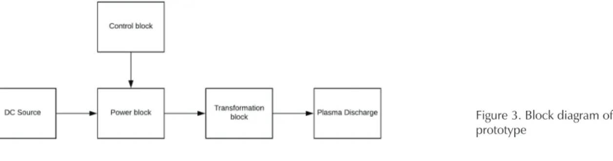
-sonant frequency of 66.75 kHz. The block diagram of the proposed prototype is depicted in Figure 3.
PowerelectronIcssourceresults a) simulation results
In order to validate the proposed circuit, the numerical
simulation of the power electronics source using Pspice
8.0 was carried out. The DC voltage is fixed at 30 V, the commutation signals have a 65 kHz frequency, as the load on the transformer secondary side a 50 kΩ resistor is used only to verify the system performance. Figure 4 shows the simulated circuit. The circuits at the bottom of the figure simulate the PWM obtained from TL494 circuit, due to, the Pspice does not have the libraries for the TL494 and the drivers IR2110. In the transformer, the parasite values (obtained with a BK PRECISION
Bench LCR/ESR 889B) are included for having more ac
-curate results. The R3 resistor simulates an isolated ground given by transformer isolation, due to its high value does not affect the simulation.
Then, in Figure 5, the output voltage and output cu
-rrent at the transformer primary is depicted. The squa-re signal squa-repsqua-resents the voltage (black color) and the quasi-sinusoidal the current signal (blue color).
0 1 1 1 (0.5) f R C =
The square signal corresponds to the inverter output,
obtaining - 30 V to 30 V, and the current is quasi-sinus
-oidal and has different phase because of the load. The current has a different scale, its real value is of 0.7 A, it
presents at the same graphic to appreciate the output waveforms.
Afterward, the voltage on the load and inverter out
-put voltage is shown in Figure 6. The square signal co
-rresponds to the transformer primary signal (black color) and the quasi-sinusoidal signal to the transfor-mer secondary (blue color).
The results obtained prove the correct performance
of the power supply, giving the desired power, enough
to generate plasma. The signal before passing the trans-former is a square signal of - 30 V to 30 V at 65 kHz, and
after the transformer, the signal becomes quasi-sinusoi
-dal of 1.3 kV, due to the parasites values.
b)
Power source constructionThe power electronics source was built following the characteristics described in section two of this
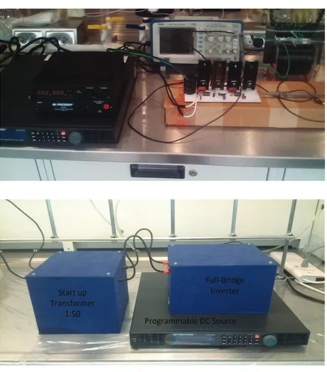
docu-ment. Figure 7 shows the full-bridge inverter prototy
-pe, corresponding to the power block and the control
block.
Then, Figure 8 depicts the experimental setup, with the DC source and the elevator transformer connected
to the full-bridge inverter.
c)
exPerimental resultsThe experimental setup previously described was
con-figured with the next values: the DC source was fixed at
40 V, and the switching frequency at 65 kHz. The volta
-ge output and the current output at the primary of the
transformer are shown in Figure 9. The current is the
quasi-sinusoidal signal and the voltage corresponds to a square signal.
The results are consisting according to the figure 4,
the inverter has a square output of - 40 to 40 V and the current is quasi-sinusoidal of 0.6 A of amplitude due to the load and have a different phase.
Then, Figure 10 depicts the voltage at the inverter
output as a square signal and the output voltage at the
Figure 4. Full-bridge inverter developed on Pspice 8.0
Figure 8. Experimental setup
Figure 7. Full-bridge inverter prototype
Table 2. Comparative between simulation and experimental results
Parameter Simulation Experimental
Frequency 65 kHz 65 kHz
Voltage input 30 V 40 V
Current 0.7 A 0.6 A
Voltage at
transformer output 1.3 kV 2 kV
secondary as a sinusoidal signal, with a high voltage and
high frequency. These results are consistent with the simu-lation results in waveform and amplitude. This guarantee enough energy power to realize the plasma discharge.
A comparative table is shown in Table 2, to present
the coherency between the results obtained by
simula-tion and experimental results, the inverter output volta
-ge is multiplied by a factor of 50 due to the transformer.
d) Plasma discharges
For proving the power electronic source in plasma
ge-neration, different plasma reactor configurations were carried out, where the equipment was inside a cabinet built with isolate material. Besides, the circuits have a
ground connection for electric discharge. The user has
to wear glasses, industrial boots, and dielectric gloves
for high voltage.
d.1) dielectric barrier discharge
Among atmospheric pressure plasma produced in
se-veral ways, the dielectric barrier discharge is mainly
characterized by the use of one or more dielectrics
dis-posed between the electrodes. This configuration pro
-duces random multifilament micro-discharges. A
high-frequency electric field is required for this purpo
-ses. The dielectric barrier distributes the micro
dischar-ge uniformly throughout the dischardischar-ge volume,
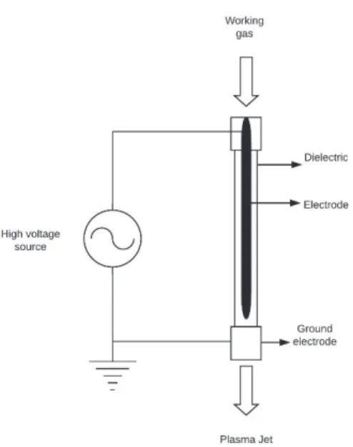
generating energetic electrons that create other active species (Jiang et al., 2018; Li et al., 2018). The diagram is depicted in Figure 11.
Using the experimental setup described above, coupled with the proposed configuration, and Helium as plasma gas, the discharge showed in Figure 12, is
obtained.
The dielectric used was a 20 cm long inert quartz cir
-cular tube, with 1.5 cm of diameter with two aluminum electrodes of 3 cm length and gap of 2 cm, the helium
provided was regulated using a needle valve. The die-lectric barrier discharges applications are well known
as etching, cleaning, thin films deposition, plasma po
-lymerization, surface treatment, materials functionali
-zation, and modification, etc.
d.2) doubles dielectric barrier discharge
The double DBD plasma is provided through a double
cylindrical dielectric barrier. This arrangement is useful to prevent arcing between the (inner) powered electro-de and a plasma exposed sample which is particularly unwanted for general applications (Florian et al., 2015;
Zhang et al., 2018). The Double dielectric reactor dia
-gram is shown in Figure 13 the purple color indicates
the plasma generated.
Then, Figure 14 shows a superior view of de Double dielectric reactor diagram, for better understanding of the configuration. The orange color denotes the ground electrode, the gray color the two dielectric barriers, and
the black color the high voltage electrode.
The double barrier dielectric reactor operation was
created, on the coaxial configuration with quartz walls
with central and external electrodes. The discharges are
operating in a 5 kHz to 150 kHz range, so the operating frequency was settled at 65 kHz (resonant frequency).
The plasma gas was helium. Figure 15, shows the dou
-ble dielectric discharge ionizing helium using the
pro-totype developed. Dielectric material presence between
both electrodes requires high AC voltages applied in a
1.2 kVp to 12 kVp, and currents from 20 to 100 mA. The power applied goes from 200 W to 1.2 kW.
d.3) Jet discharge
One of the cold atmospheric plasma sources is jet type,
which can generate plasmas in open space rather than in
confined discharge gaps and it is characterized by flexi
-bility, compactness, and efficiency (Fan et al., 2012). The
Jet plasma reactor diagram is depicted in Figure 16. In order to produce discharges without electric arcs,
-ges at 15 kVp and operation frequencies for 5 to 150 kHz. On jet plasma discharge a shining on the reactor
extreme is produced. This shining is used for material treatment and modifying the material structure. The
plasma generation was configured under parameters shown in Table 2.
With the parameters stated above, the plasma dis
-charge obtained on a jet type reactor is shown in Figure 17, at atmospheric pressure.
Figure 11. Dielectric plasma reactor diagram
Figure 14. Superior view of double dielectric reactor diagram
Figure 15. Double dielectric barrier discharge
Table 3. Jet reactor parameters
Voltage 15 kVp
Current 20 mA
Power 300 W
Plasma global temperature < 70 °C
Plasma gas Air
Air flux 6 LPM
Figure 16. Jet type plasma reactor diagram
conclusIons
The power electronic source developed allow varying
the operating frequency from 5 kHz to 150 kHz, and a
duty cycle from 0 to 47 %. It is coupled to a BK PRECI
-SION XLN10014 programmable DC source, and a ge
-neral purpose star up transformer to provide until 15 kVp at 1.4 kW of power. The variable frequency allows
to syntonizer the natural resonance zone, and it is im
-portant because the regions of maximum voltage
am-plification aids to ignite and generate stable plasma
discharges.
The experimental prototype design was first tested
by numerical simulations and then it was built
physica-lly, the results in both, simulation and physical are con
-sistent and coherent.
The designed prototype is useful to generate plasma
discharges, which can help to modify materials, in order
to enhance electrical, mechanical, and thermal proper
-ties. The proposed prototype has an electronic control
that allows varying some parameters like frequency, and
duty cycle, this are some advantages against plasma ge
-neration through radiofrequency, and microwave.
Plasma discharges were made for ionizing helium
on two different reactor configurations: dielectric ba
-rrier, double dielectric ba-rrier, and ionizing air on a jet type reactor. In all of them, it was possible to achieve an electrical field strong enough to reach the breakdown
voltage and generate plasma discharge.
The system advantage presented in this work against other high voltage source for plasma
genera-tion, is the versatility to generate plasma at vacuum and atmosphere pressure, with electrodes on direct contact
to the plasma or through dielectric discharges.
As future work is proposed to implement a fee-dback nonlinear control as sliding mode control or fuzzy
control, to improve the prototype features, the system is in open loop, and also taste the plasma generated to
modify materials.
acknowledgements
This work was partially supported by CONACYT through the Ciencia Básica grant No. 288682 under the direction of Ku-Herrera J.J. and in part by grant 299092 Laboratorio Nacional en Innovación y Desarrollo de
Materiales Ligeros para la Industria Automotriz (LA
-NIAUTO). The authors would like to thank Sierra U.,
Méndez G., Lozada M. and Mercado A. for their inva
-luable technical support.
references
Birle M., Leu C. & Bauer S. (2011). Design and application of a high-frequency high-voltage generator. On Internations Sym
-posium on High Voltage.
Fan Q.Q., Qian M.Y., Ren C.S., Wang D. & Wen X. (2012). Dischar
-ge characteristics of a cold-atmospheric-plasma jet array -gene
-rated with single electrode configuration. IEEE Transactions on Plasma Science, 40 (6), 1724-1729. https://doi.org/10.1109/ TPS.2012.2191307
Florian J., Merbahi N., Florian J., Merbahi N., Wattieaux G., Plewa J.M. & Yousfi M. (2015). Comparative studies of double dielec
-tric barrier discharge and microwave argon plasma jets at at -mospheric pressure for biomedical applications. IEEE Transactions on Plasma Science, 43 (9), 3332-3338. https://doi. org/10.1109/TPS.2015.2404879
Hnautic E., Astanei D., Ursache M. & Hnautic B. (2012). A review over the cold plasma reactors and their applications. On 2012 International Conference and Exposition on Electrical and Power Engineering (EPE 2012), IEEE, 497-502. Retrieved
from https://doi.org/10.1109/ICEPE.2012.6463884
Jiang H., Shao T., Zhang C., Yiang P. & Liu H. (2018). Two typical
charge transportation characteristics in nanosecond-pulse surfa-ce dielectric barrier discharge. IEEE Transactions on Plasma Scien-ce, 46(10), 3524-3530. https://doi.org/10.1109/TPS.2018.2811728
Juárez M.A., Vázquez G., Sosa J.M., Martínez P.R. & García F. (2016). Analysis and design of resonant inverter for ozone ge
-neration. On 2016 IEEE International Autumn Meeting on Power, Electronics and Computing (ROPEC). Retrieved
from https://doi.org/10.1109/ROPEC.2016.7830644
Karys S. (2009). Selection of resonant circuit elements for the ARCP inverter. On 2009 10th International Conference on Elec
-trical Power Quality and Utilisation. Retrieved from https:// doi.org/10.1109/EPQU.2009.5318855
Kim Y.M., Kim J.Y., Jo M.C., Lee S.H., Mun S.P., Lee H.W., Kwon S.K. & Sun K.Y. (2006). Resonance inverter power system for improving plasma sterilization effect. On 2006 CES/IEEE 5th International Power Electronics Conference. Retrieved
from https://doi.org/10.1109/IPEMC.2006.4778248
Levchenko I., Cvelbar U. & Keidar M. (2016). Graphene flakes in
arc plasma: conditions for the fast single-layer growth. Gra-phene, 5(2), 81-89. https://doi.org/10.4236/graphene.2016.52009
Li X., Chu J., Jia P., Li Y., Wang B. & Dong L. (2018). Characterization
of a laminar plasma plume based on dielectric-barrier discharge at atmospheric pressure. IEEE Transactions on Plasma Science, 46 (3), 583-586. https://doi.org/10.1109/TPS.2018.2797954
Millner A.R. (2008). Power electronic topologies for plasma gene
-rator. On 2008 International Symposium on Industrial Elec
-tronics, 359-362. Retrieved from https://doi.org/10.1109/ ISIE.2008.4676925
Ren F., Ji S., Hao Z. & Shi Y. (2016). Study of the characteristics of cold air atmospheric pressure plasma jet generated with in -verted tapered tube. IEEE Transactions on Plasma Science, 44 (11), 2594-2602.https://doi.org/10.1109/TPS.2016.2598418
Schutze A., Jeong J.Y., Babaya S.E., Park J., Selwyb G.S. & Hicks R.F. (1998). The atmospheric-pressure plasma jet: a review and com -parison on the other plasma sources. IEEE Transactions on Plasma Science, 26(6), 1685-1694. https://doi.org/10.1109/27.747887
Tendero C., Tixier C., Tristant P., Desmaison J. & Leprince P. (2006). Atmospheric pressure plasmas: A review. Spectrochimi-ca Acta-Part B: Atomic Spectroscopy, Elsevier, 61 (1), 2-30. https:// doi.org/10.1016/j.sab.2005.10.003
Wang K., Xu M., Gu Y., Gu Z., Liu J. & Fan Q.H. (2017). Low tem -perature plasma exfoliated n-doped Graphene for symmetri-cal electrode supercapacitors. Nano Energy, Elsevier, 31, 486-494. https://doi.org/10.1016/j.nanoen.2016.11.007
Zhang X., Xiao H., Hu X. & Zhang Y. (2018). Effects of reduced elec
-tric field on sulfur hexafouride removal for a double dielec-tric
barrier discharge reactor IEEE Transactions on Plasma Science,