THE DEVELOPMENT OF AN ANDROID APP AS A TOOL FOR LEARNING AND DESIGNING DCDC CONVERTERS
6
0
0
Texto completo
(2) THE DEVELOPMENT OF AN ANDROID APP AS A TOOL FOR LEARNING AND DESIGNING DC-DC CONVERTERS 1 INTRODUCTION The use of wireless technology allows learners to have access to information and learning material no matter the place or the moment. For this reason, wireless technology has given learners full control over when and where they want to learn (ALLY, 2009; KEARNEY et al., 2012) Most of the learning objects are implemented in traditional platforms as desktop computers or laptops. Today, mobile devices (smartphones and tablets) are being improved at a hardware and software level with relatively low costs. For this reason, the development of tools that support the learning process focuses on these mobile devices can be considered worthwhile (ARISTIZABAL; ALMARIO; LOPEZ, 2014). The development of the proposed app rises as a strategy for reducing the complexity in order to obtain accurate calculations to design DC-DC converters, such as the Buck, Boost and Buck-Boost converters. Thus, providing easy access to full development within minutes of use. Beyond that, this app also presents a special activity for the advanced results of the project. It provides information about the value of critical inductance to achieve the continuous conduction mode, the project of Snubber and the full design of an E-Core inductor. Finally, the software also facilitates understanding the subject for new students in the power electronics area, containing all the main concepts of the object of study. 2 METHODOLOGY This app was developed using the software development environment Android Studio IRU *RRJOH¶V $QGURLG RSHUDWLQJ V\VWHP, built based on the Java programming language, with the help of Corel Draw software to create the figures present in the activities. In addition, the Matlab software was also used to create the code routine for the E-Core inductor design. In order to construct the graphs present in the information activity, the LTspice software was used. Figure 1 presents a flow chart of the implemented app. For the development of the Main Calculations, it was used as input the following parameters: Input Voltage (V), Output Voltage (V), Power Output (W), Ripple Inductor Current (%), Ripple Capacitor Voltage (%), Efficiency (%) and finally the Frequency (kHz), for the operation of the PWM (Pulse-Width Modulation). In order to obtain the results, access to the Reverse Engineering and Information, was used virtual buttons. ,I WKH XVHU KDV DFFHVV WR WKH FRQYHUWHU¶V FRPSRQHQWV YDOXHV DQG ZDQWV WR NQRZ LWV RXWSXW SRZHU IRU H[DPSOH RQH FDQ XVH WKH ³UHYHUVH HQJLQHHULQJ´ activity. The following input variable are requested: Input Voltage (V), Output Voltage (V), Inductance (mH), Capacitance (uF), Resistance (Load) (Ohms) and Frequency (kHz). The selection buttons were implemented in the same way of the main section. The values used are the same of the main section for the Boost converter project. $ ³'HILQLWLRQV´ SDJH DV DOVR DGGHG WR WKH DSS ,Q WKHVH VHFWLRQV DOO LQIRUPDWLRQ RI WKH study object will be presented. It will contain explanations for each step of the project developed, detailing the operation of the converters, Snubber and considerations for the E&RUH LQGXFWRU GHVLJQ %HVLGHV WKDW DOVR LW ZDV DGGHG D VXE DFWLYLW\ ³6\PEROV´ WR GHVFULEH each symbol used during the steps of the app. Anais do 10º SALÃO INTERNACIONAL DE ENSINO, PESQUISA E EXTENSÃO - SIEPE Universidade Federal do Pampa œ Santana do Livramento, 6 a 8 de novembro de 2018.
(3)
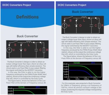
(4) 3.2. Reverse Engineering. The ³5HYHUVH (QJLQHHULQJ´ section is demonstrated at the Figure 4. From the selected ³5HYHUVH (QJLQHHULQJ´ EXWWRQ DW WKH PDLQ DFWLYLW\ WKH QH[W SDJH is shown by Figure 5. The results obtained are Power Output (W), Ripple Inductor Current (%), Ripple Capacitor Voltage (%) and Duty Cycle (%). Figure 4 ± Reverse Engineering. Source: Author, 2018.. 3.3. Figure 5 ± Reverse Engineering results. Source: Author, 2018.. Definitions. Figure 6 illustrates this section, demonstrating how it will be the explanation of the Buck converter. Beyond that, Figure 7 demonstrates the activity "Symbols" which demonstrates all the symbols used in the figures present in the application. 3.4. Advanced Calculations. From de results pages, one can then proceed to the advanced calculations, Figure 8, VHOHFWLQJ WKH ³$GYDQFHG´ EXWWRQ LQGependently of the mode select. The results include the following parameters: Critical Inductance, Input Current, Output Current, Switch Current, Diode Current, Inductor Current Variation (A), Capacitor Voltage Variation (V). The conduction mode obtained from the project is also presented in this page. It is important to highlight that this app was developed to design converters at the continuous conduction mode. Thus, the advanced calculations results can only be applied to such conduction mode and should be disregarded for any other. If the configuration is such that the obtained conduction mode is discontinuous, the project needs to be restarted and the inductor value must be greater than the critical value calculated, resulting in continuous conduction mode. The figure also shows the buttons for access the pages of Snubber and E-Core inductor project. 3.4.1 Snubber Project Based on these values, it is possible to calculate the Snubber, which must be fill with two input values, Time Delay Off (ns) and Time Delay Fall (ns). These values are found in Anais do 10º SALÃO INTERNACIONAL DE ENSINO, PESQUISA E EXTENSÃO - SIEPE Universidade Federal do Pampa œ Santana do Livramento, 6 a 8 de novembro de 2018.
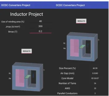
(5) the datasheet of the switch that will be used in the converter design. For this example, it was used the MOSFET IRF740. The activity is show in Figure 9. Figure 6 ± Concepts definitions. Source: Author, 2018.. Figure 8 ± Advanced Calculations. Source: Author, 2018.. Figure 7 ± Symbols activity. Source: Author, 2018.. Figure 9 ± Snubber Project. Source: Author, 2018.. 3.4.2 E-Core Inductor Project 6HOHFWLQJ WKH ³,QGXFWRU 3URMHFW ( &25( ´ LQ WKH $GYDQFHG &DOFXODWLRQV DFWLYLW\ WKH next page is shown by Figure 10, where is possible to obtain the full project of an E-Core inductor for the required converter. In this page, the following values are requested for the input data: Use of winding area (%), Jmax (A/mm²) (Maximum Current Density) and Bmax (T) (Maximum Flux Density). This section still in development, but a demonstration is shown by Figure 10. The partial results are Size Percent (%), Air Gap (mm), Core Model, Number of Turns, American Wire Gauge (AWG) and Numbers of Parallel Conductors. Anais do 10º SALÃO INTERNACIONAL DE ENSINO, PESQUISA E EXTENSÃO - SIEPE Universidade Federal do Pampa œ Santana do Livramento, 6 a 8 de novembro de 2018.
(6) Figure 10 ± Inductor Project. Source: Author, 2018.. 4 FINAL CONSIDERATIONS From the presented data, it is possible to observe the facility and practicality that the application has the potential to bring to anyone who needs to design a DC-DC converter, from the most basic parameters to the complete Snubber design and the E-Core inductor. One of the main objectives of this software, besides establishing a practical means for the design of converters, is to make accessible the understanding of this area of power electronics, even if the user does not understand the subject, can still learn and train the design of a DC-DC converter within the application itself. Taking into consideration the initial stage of development, there is still much to improve, seeking to implement more functions and making it more complete with each update. REFERENCES ALLY, Mohamed. Mobile Learning Transforming the Delivery of Education and Training. [s.l: s.n.]. v. 3 ARISTIZABAL, Leandro Florez; ALMARIO, Diego F.; LOPEZ, Jesus A. Development of an Android App as a learning tool of dynamic systems and automatic control. 2014 III International Congress of Engineering Mechatronics and Automation (CIIMA), [s. l.], p. 1±5, 2014. Disponível em: <http://ieeexplore.ieee.org/document/6983438/>. KEARNEY, Matthew et al. Viewing mobile learning from a pedagogical perspective. Research in Learning Technology, [s. l.], v. 20, n. 1, p. 0±17, 2012.. Anais do 10º SALÃO INTERNACIONAL DE ENSINO, PESQUISA E EXTENSÃO - SIEPE Universidade Federal do Pampa œ Santana do Livramento, 6 a 8 de novembro de 2018.
(7)
Figure

Documento similar
If the electrolytic capacitor of an AICS is removed, then low-frequency ripple arises at its intermediate dc bus, adding some distortion in the line input current over the
The power processing circuit (PPC) created by the evolutionary algorithm is connected on one side to an input voltage source V in , and on the other side to an output circuitry made
rGO-ODA was used as a filler in the preparation of TFN membranes using two different concentrations in the organic phase for the interfacial polymerization: 0.03% (w/v) and
It is distinguished two ways of efficiency measurement: in the direct method, the input and output power are measured directly, as the expression (2); and the indirect
of emissions. Likewise, since official data informs about emissions generated by domestic production, this region should actually be less responsible for the environmental
The output op-amp IC2 is used as a summing amplifier with the CAMAC DAC derived velocity demand connected to the -ve input and the drive motor tachometer feedback to the +ve
Many active input current shapers [l-61 have been proposed in this way to avoid the traditional drawback of poor dynamic output voltage reguIation thanks to its fast
The principle behind this meth- od shown in Figure 1 is to create the desired channel model by positioning an arbitrary number of probe antennas in arbitrary positions within
