ESCUELA T ´
ECNICA SUPERIOR DE INGENIEROS
DE TELECOMUNICACI ´
ON
PROYECTO FIN DE GRADO
DESIGN AND SIMULATION OF A COHERENT
TRANSMITTER BASED ON A PHOTONIC
INTEGRATED CIRCUIT FOR INTER AND INTRA
SATELLITE COMMUNICATIONS
ALICIA SORIA G ´
OMEZ
SERVICIOS DE LA TELECOMUNICACI ´
ON
TRABAJO FIN DE GRADO
T´ıtulo: DESIGN AND SIMULATION OF A COHERENT TRANSMITTER BASED ON A
PHOTONIC INTEGRATED CIRCUIT FOR INTER AND INTRA SATELLITE COMMUNICATIONS
Autor: D.a Alicia Soria G´omez
Tutor: D. Antonio P´erez Serrano
Departamento: Departamento de Tecnolog´ıa Fot´onica y Bioingenier´ıa (TFB)
MIEMBROS DEL TRIBUNAL
Presidente:
Vocal:
Secretario:
Suplente:
Los miembros del tribunal arriba nombrados acuerdan otorgar la calificaci´on de:
Escuela T´
ecnica Superior de Ingenieros de
Telecomunicaci´
on
Proyecto Fin de Grado
Design and simulation of a coherent transmitter
based on a photonic integrated circuit for inter
and intra satellite communications
Alicia Soria G´
omez
Nowadays satellites handle an enormous amount of information. On one hand, each satellite contains numerous instruments that interchange information inside them. On the other hand, satellites communicate with the ground control and between each other, especially in satellite systems. Therefore, being able to manage high bit rates is becoming a necessary feature in any satellite. However, satellites are costly. Launching one kilogram into space can be priced at 25k euros. Therefore, the size and weight of every component in a satellite are crucial.
Optical communications systems are a suitable solution for inter and intra satellite communications. These systems are based on transmitters and receivers fabricated using semiconductor materials. These photonic devices, especially semiconductor lasers, show advantages that fit on the satellite requirements, such as electrical pumping, high efficiency, compactness, radiation hardness and low cost. In the last years, semiconductor lasers have shown another advantage, the integration of different optical components such as lasers, modulators, photodiodes, amplifiers, etc. in the same chip. If the number of these components is high, these devices are called photonic integrated circuits, in analogy to electronic integrated circuits.
The objective of this work is to design a coherent transmitter based on a photonic integrated circuit containing a multi-section laser and an IQ modulator that can be used as a transmitter for intra and inter satellite optical communications. The design is validated through numerical simulations and the final design will be fabricated by means of an open access foundry. Regarding the multi-section laser, a four-section distributed Bragg reflector laser has been chosen as the most appropriate to be integrated in the photonic integrated circuit.
It is designed with the main objective of being a tunable single-mode emitter. The parameter de-pendence on each of the four sections of the laser is analyzed and thoroughly characterized in terms of power and wavelength tuning. With respect to the IQ modulator, a first step involves the analysis of electro-optical-phase-modulators. After that, the design and characterization of different Mach-Zehnder modulators is done. Finally, two versions of the IQ modulator are designed, for high (up to 10 GHz) and low (up to 250 MHz) frequency RF signals and several parameters such as attenuation and the induced phase shifts are thoroughly analyzed.
Finally, both modules are integrated into the coherent transmitter and the layout of the different ver-sions of the chip are designed. The layout contains all the different material layers as well as the electrical routing and optical outputs. The layout is the final design result which is sent to the foundry for fabrication.
Key words: optical communications, photonic integrated circuit, PIC, IQ modulator,
Hoy en d´ıa, los sat´elites manejan cantidades ingentes de informaci´on. Por un lado, cada sat´elite est´a formado por m´ultiples componentes que intercambian datos, y por otro, los sat´elites se comunican con estaciones en tierra y entre ellos. Por tanto, la capacidad de manejar grandes cantidades de datos se ha convertido en una caracter´ıstica fundamental para estos sistemas. Sin embargo, la tecnolog´ıa satelital es muy costosa y lanzar un kilo de material al espacio puede alcanzar los 25k euros, por lo tanto, es crucial el tama˜no y peso de cada componente del sistema.
Las comunicaciones ´opticas son una tecnolog´ıa apropiada para las comunicaciones inter e intra satelitales. Los sistemas ´opticos est´an compuestos por transmisores y receptores fabricados con materiales semiconduc-tores. Sus caracter´ısticas son especialmente adecuadas para su integraci´on en los sistemas satelitales: su bombeo es el´ectrico, muestran una alta eficiencia, robustez, compacidad, resistencia a la radiaci´on y tienen un bajo coste. En los ´ultimos a˜nos, la tecnolog´ıa de semiconductores ha logrado integrar distintos elemen-tos optoelectr´onicos en un mismo chip, tales como l´aseres, moduladores, fotodiodos, amplificadores, etc. Estos dispositivos se denominan ”circuitos fot´onicos integrados”, en analog´ıa con los circuitos electr´onicos integrados.
El objetivo de este proyecto es dise˜nar un transmisor coherente basado en un circuito fot´onico integrado que contiene un l´aser multi- secci´on y un modulador IQ que pueda ser usado en sistemas de comunicaciones inter e intra satelitales. El dise˜no est´a respaldado por simulaciones num´ericas y el resultado final se ha enviado a un fabricante de acceso abierto para su fabricaci´on. Con relaci´on al l´aser multi secci´on, se ha elegido un l´aser de cuatro secciones que contiene reflectores distribuidos de Bragg debido a sus propiedades y capacidad de integraci´on en el chip. El objetivo del dise˜no es obtener un l´aser sintonizable mono modo, cuya dependencia con los par´ametros ha sido analizada y caracterizada en cada una de las cuatro secciones, entre ellos se ha prestado especial atenci´on a la potencia y la sintonizaci´on de su longitud de onda de emisi´on. Para el dise˜no del modulador IQ se han seguido varios pasos. En primer lugar, se han analizado moduladores de fase electro- ´opticos y caracterizado varios moduladores Mach-Zehnder. Caracter´ısticas como la atenuaci´on y los desfasajes inducidos han sido analizados. Finalmente, se dise˜naron dos versiones del modulador IQ, el primero de ellos apropiado para una frecuencia de modulaci´on elevada (hasta 10 GHz), y el segundo para bajas frecuencias (hasta 250 MHz).
Finalmente, ambos dispositivos se han integrado en el transmisor coherente y dise˜nado el ”layout” de las distintas versiones de los chips. El layout incluye la distribuci´on de las distintas capas de los materiales, as´ı como el enrutado el´ectrico y la localizaci´on de las salidas ´opticas. Este dise˜no final es el resultado de todo el proceso de dise˜no y ha sido enviado para su fabricaci´on.
Palabras clave: comunicaciones ´opticas, circuitos fot´onicos integrados, PIC, modulador
1 Introduction 1
1.1 Optic communications . . . 1
1.2 Inter and intra satellite communications . . . 3
1.3 Photonic Integrated Circuit technology . . . 4
1.4 Motivation and objectives . . . 6
1.5 Summary . . . 7
2 Methodology 9 2.1 Design flow . . . 9
2.2 Software used and manufacturing . . . 10
2.2.1 SMART Photonics B.V. . . 10
2.2.2 VPIphotonics Design Suite . . . 11
2.2.3 Nazca Design . . . 17
3 Four section DBR Laser 18 3.1 Semiconductor lasers . . . 20
3.1.1 Fabry-P´erot cavity . . . 21
3.1.2 Bragg gratings . . . 23
3.1.3 Distributed Bragg reflector lasers . . . 23
3.2 Laser design and analysis . . . 24
3.2.1 Calculated dimensions and parameters . . . 25
3.3 Laser simulations . . . 27
4 IQ modulator design and analysis 34 4.1 Mach-Zehnder modulator . . . 35
4.1.1 MZM design . . . 35
4.1.2 MZM simulations . . . 37
4.2 IQ module . . . 40
4.2.1 QPSK modulation . . . 40
5 Photonic Integrated Circuit layout 43 5.1 Physical characteristics . . . 43
5.2 Design rules . . . 43
5.3 Low frequency PIC . . . 45
5.4 High frequency PIC . . . 45
5.4.1 Simulations . . . 47
5.5 Fabricated PIC . . . 47
6 Conclusions and future lines 49 6.1 Conclusions . . . 49
Appendices 54
A Ethical, economic, social and environmental aspects 55
A.1 Introduction . . . 55
A.2 Relevant impacts of the project . . . 55
A.2.1 Environmental impact . . . 55
A.2.2 Social and ethical impacts . . . 55
A.3 Economic impact in detail . . . 56
A.4 Conclusions . . . 56
B Economic budget 57 C Python codes 59 C.1 Low frequency PIC . . . 59
Introduction
Nowadays the 53.6 % of the world population has access to the Internet, which means 4.17 billion people sending and receiving messages, calls, videos, etc. We are growing towards a paradigm in which all parts of the world are connected, and here, satellites play a vital role. Furthermore, satellite communication also appears in breakthroughs such as the management of 5G networks, recovery of disasters, remote sensing, etc. According to Houlin Zhao, most industries depend in a way or other on satellite technology, from agriculture to bank and transportation1.
This increase in the number of available apps means a growing necessity for capacity and data speed, which is leading to the congestion of the RF spectrum [1]. Therefore, alternatives are being explored such as optic communications in satellite systems.
1.1
Optic communications
During the last 20 years optic communications have been experiencing a major growth in satellite applica-tions. There are two different methods in which this integration is accomplished. The first method is Optic Fiber Communication (OFC), which is the evolution of copper cable as a carrier of information, and the second method is Optical Wireless Communications (OWC), it involves the transmission of information through a light beam across free space, without using transmission guides.
OFC involves the transmission of light signals through a glass or plastic fiber which consists on a fiber core surrounded by a cladding. Typical values for their refractive indexes are ncladding = 1.48 and
ncore= 1.5, which allows light to bounce against the cladding while being confined inside the fiber [2]. Op-tical fibers can be divided according to their refractive indexes, polarization, dispersion, number of modes, etc. This last category is split into single-mode fibers and multi-mode fibers. In single-mode fibers the core diameter ranges from 8 to 10µm, while the cladding diameter typically measures 125µm, this represents a very narrow core in which the one-wavelength-light beam is confined. Generally, a highly precise laser is employed to transmit the light signal, as the laser emits a monochromatic, low divergence beam and higher bandwidth signals as well as higher bitrates can be achieved than in multi-mode fibers. On the other hand, multi-mode fibers contain a core of diameter either 50 or 62.5µm, while the cladding diameter is 125µm. Multi-mode fibers are more affordable than single-mode fibers and they can apply a LED as the transmitting module. The applications of OFC aside from satellite communications are diverse. Amongst them: broadcast, internet provider, telephone services, space applications, medical uses, etc. due to the multiple advantages that they present when compared to cable communications.
Their most relevant characteristics are higher bandwidth, maximum throughput increases from 10 Gbps using copper to 10 Tbps with optical fiber; less attenuation, therefore, the signal can be transported further, from 5 km with copper at 1 Gbps to 20 km with fiber at 1 Tbps; additionally, electromagnetic interference is practically harmless, hence less spacing between cables is needed, and finally weight can be reduced up to a tenth when using optical fibers, which is particularly interesting for space applications [3].
OWC are not as widespread as OFC. The beginning of OWC dates back to 1810, when C. F. Gauss handled two mirrors to reflect and guide a beam of sunlight. Through the years several experiments were performed, for instance, the photo phone [4] of A. Graham Bell, in which modulated beams of light were manipulated to transmit speech. OWC can be divided intovisible light communications (VLC) andfree space optics (FSO) which involves the transmission of information through free space, either in ground-satellite, satellite-ground, satellite-satellite links, or deep space (see Fig. 1.1).
Figure 1.1: Scenarios where optical communications are employed
VLCs are generally employed on the Earth surface. They operate with a LED as a transmitter in the band of 390-750 nm, and are used in wireless local area and personal networks. On the other hand, FSO main application is communications with satellites, Unmanned Aerial Vehicles (UAV) or deep space exploration. They employ laser emitters and operate in the band of 750-1600µm, though advances have been made in the band of 200-280 nm [5].
Both optical communication systems mentioned before (OFC and OWC systems) are composed at least of three sections: transmitter, receiver and transmission line [6].
The transmitter is a module that receives an electrical signal and converts it into a light signal,
usually semiconductor modules such as LEDs or lasers are employed, as well as modulators.
The receiveris typically a semiconductor-based photodiode which receives the beam of light and
con-verts it to electricity due to the photoelectric effect. This principle was resolved by Einstein in 1905 and explains why some materials are able to emit ions or electrons when they absorb electromagnetic radiation, thus producing electricity when a beam of light falls upon them [7].
The transmission line is an optical fiber made of glass or plastic through which light travels by
reflections inside its core. Free space and the atmosphere can also be employed as transmission mediums.
1.2
Inter and intra satellite communications
Satellite systems involve information transmission between satellites known asinter satellite communica-tionsand inside one satellite, called intra satellite communications (see Fig. 1.1).
Inter satellite communications are based on FSO. Research on FSO dates back to 1967 with the studies of Fried [9] in optical uplink transmission. Through the years, several experiments were carried out, such as the Galileo optical experiment in 1992 [10] in which two laser signals were sent from New Mexico and California to a deep space vehicle at 1.4 million kilometers, in order to measure atmosphere turbulences. However, it was not until 2005 when the European Space Agency (ESA) demonstrated the first inter-satellite laser link between the satellites SPOT-4 and ARTEMIS. Since then, several other projects were successful among the military and exploration missions in aerospace laboratories, for instance, the STROPEX project, in which an optical high bit rate downlink was established between a HAP2 and a ground station in 2004 in UK thanks to the CAPANINA project [11]; another example is the Mars Laser Communication Demonstration (MLCD) by NASA and MIT3 in 2009 which proved a 10 Mbps down and uplink between Earth and Mars.
FSO are deemed as the future of communications due to the multiple advantages they present when compared to RF communications. The main reason for these advantages roots in the fact that optical communications make use of carriers in a higher frequency that RF, therefore the wavelength is smaller. Amongst them we can find:
1. High bandwidth: bandwidth is proportional to the carrier frequency, which means that the bit rate can increase proportionally.
2. Less power requirements: as the divergence of a laser beam is proportional toλ/Dr (where Dr is the aperture diameter and λ is the wavelength), therefore, the received signal has more intensity than compared to a RF transmitter.
3. High directivity: directivity is inversely proportional to beam divergence
4. Free from licensed spectrum: radio frequencies coexist in the same spectrum range, so bandwidth is very limited and expensive, this does not affect optic communications for now.
5. Security: as laser beam is narrow, it is more difficult to detect.
6. Light weight and compact
7. Reduced size of network segments: small-scale components are used, and free space is the medium through which light travels, hence, there is no need for that optics system segment.
8. Easily deployable: as infrastructure does not have to be altered in order to set up the optical system, for example, it is necessary to dig the streets to distribute cable systems.
9. Relatively low cost: component size is small, and most materials used are affordable (such as silicon) so fabrication cost is not excessive.
However, there are some drawbacks when making use of FSO. These include atmospheric absorption and scattering losses, due to the fog, rainfall, air molecules, haze, etc, turbulences due to changes in temperature and pressure, misalignments in the beam due to satellite vibrations and atmospheric turbulences, doppler
2High Altitude Platforms are airborne stations such as zeppelins and balloons
shift, etc. These problems are highly dependent on the carrier frequency and are especially important in higher frequencies, therefore FSO communications are critically affected as they work in the wavelength ranges of 780-850 nm and 1520-1600 nm. Evidently, researchers have developed various mitigation tech-niques to solve these problems. For example, atmospheric turbulences are mitigated when using aperture averaging, a technique that increases the size of the receiving aperture by considering the fluctuations in the laser beam [1]. Another innovative technique is adaptative optics, also used to reduce the effect of atmospheric turbulences, it consists of a closed loop where the turbulences are considered before emission, and the signal is then transmitted with atmospheric turbulence compensation. Apart from the techniques mentioned before, the use of modulations, encoding and hybrid RF/FSO systems is recurrent [1].
FSO communications are and will be used in Earth and deep space communications. They have proved to be an improvement in comparison to RF systems, in terms of deployability, bit rate, cost and size, which are able to meet the needs of speed and capacity of an increasingly growing technological population.
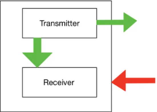
Intra satellite communication on the other hand can employ either FSO or OFC. Though many satellite systems still include rigid connections, subsituting on board cables with optical wireless links offers many advantages such as reduction of electromagnetic interference, distribution flexibility, adaptable signal rout-ing, increased connectivity, etc. [12]. Nowadays on board modules usually include novel technologies such as adaptive encoding, complex noise canceling technologies, thorough equalization technologies, adaptative modulation, etc. [13]. Increasingly, transceivers following the scheme in Fig. 1.2 are being implemented into the optical systems.
Figure 1.2: Schematic of a transceiver for inter and intra satellite communications
1.3
Photonic Integrated Circuit technology
The advantages referring to the physical structure of the optic system are the following: light weight and compact structure, small-scale components, easily deployable and finally, and affordable cost. The approach to solving these topics materializes in millimetric-dimension devices known as Photonic Integrated Circuits (PICs). PICs are “the integration of a large number of optical devices on a small substrate, forming an optical circuit reminiscent of the integrated circuit on microelectronics” [14]. It is a requirement that a PIC should have at least two different functional sections integrated, and they should be connected by a waveguide [15]. However, nowadays PICs integrate up to thousands of different functional sections.
the sizeable solid-state lasers and gas lasers. Throughout the years, semiconductor lasers were used as discrete components, and it was not until 1987 when a laser and a modulator were integrated into the same circuit. However, the design of every component and their further integration into a wafer involved a vast amount of detailed work; this setback was solved in the 2000s when the JePPIX institute [16], the first foundry for InP was pioneer in generic integration, based in the creation of standard building blocks which can be integrated into a wafer. Finally, in 2007, a large percentage of the ePIXnet4 partners adopted this measure. This meant a common base of photonic integrated circuits research in Europe [17].
Nowadays, PIC development finds itself as electronic integrated circuits did in the 1970s. Luckily, investment from governments and institutes is becoming more noticeable over the years. PICs are expected to lead the optical system industry in the following years. Their applications will be various, for instance: optical transmitters tunable frequencies, biosensors based on refractive index detection, LIDAR5, etc. [19] Common materials used for PIC fabrication and some of their applications follow:
Silicon (Si): waveguides, directional couplers, low efficiency Raman lasers.
Silica (SiO2): employed for waveguides, couplers, power splitters, combiners, etc. They can also be
connected to optical fibers.
Indium phosphide (InP): arrayed gratings, waveguides, photodiodes, amplifiers. Generally used in 1500 nm wavelength.
Gallium arsenide (GaAs): similar functionalities as InP.
Rare-earth-doped glasses: lasers and amplifiers. Usually work in 900-1080 nm.
Lithium niobate (LiNbO3): electro-optic modulators, waveguides. It is particularly interesting for
po-larization control due to its birefringence characteristics which allow for refractive index modification with light polarization.
Figure 1.3: PIC1 design 2019 from CEMDATIC-UPM
4European Network of Excellence on Photonic Integrated Components and Circuits, created in 2004 by the European
Commission to stimulate photonic integration investigation
The most popular materials for PIC substrate fabrication are InP and silicon. Each technology has certain advantages and throwbacks.
Silicon over insulator (SOI) is widely extended for its competitive cost and easy scalability into greater volumes. Furthermore, electric integrated circuits are also built on silicon wafers, therefore electro-optic device integration is easily achievable [20]. Nonetheless, silicon does not hold the required physical prop-erties for laser and amplifier fabrication because its efficiency is low, as it is an indirect transition material in which energy is lost as heat when electrons fall to a lower energy band. Conversely, InP allows for laser and amplifier fabrication, and manifests a greater efficiency, however, electro-optic integration is more challenging and notably more costly. In the near future, the chosen path will be hybrid integration of both materials [21].
A major advantage offered by foundries is the creation of Multi-Project Wafers (MPW). They consist in the generic integration of different projects in the same wafer, which allows for the division of costs among the users and fewer fabrication cycles, as projects are compressed into a single wafer (see Fig. 1.4) .
Figure 1.4: Multi Project Wafer (from [22])
A close-up of a PIC can be seen in Fig. 1.3. It included four section lasers, modulators, optical waveg-uides and electrical gwaveg-uides and electrical pads.
PIC development is a buoyant business nowadays, major players in the market include Avago Tech-nologies, Infinera Corporation, Mellanox TechTech-nologies, Ltd., Luxtera Inc., Huawei Technologies Co., Ltd., Hewlett Packard. The photonic integrated circuit industry is expected to reach the estimated market value of USD 1492.4 million in 2023, from 385.5 million in 2017. With this economic growth in mind, industry involved companies have begun a technological race and established alliances, for instance, MACOM and GF (Global Foundries) joined forces in March 2019 in order to boost photonic integrated circuit indus-try development, which directly affects 5G networks and hyperscale data centers [23]. An example of a commercial PIC belongs to Infinera, an illustration of their PIC is given in Fig. 1.5
Currently, the two academic centers leading investigation in PIC development are the University of California at Santa Barbara, USA and the Eindhoven University of Technology, Netherlands.
1.4
Motivation and objectives
Figure 1.5: Infinera 1.2 Tb/s coherent transceiver module, 6 channels, 16 QAM
information wirelessly, without guided transmission lines. However, in 1960 light began to be investigated as an efficient alternative for unguided communications, hence, and term “optical communications” was coined. This will serve as the vehicle to learn about optical wireless communications and systems in free space and in the Earth surface, as well as optical communications confined into a medium. It will be useful to acquire knowledge light wave properties and the techniques employed to compensate undesirable factors that affect it while carrying information, as well as to gain insight into the materials employed and their characteristics.
The main objective consists in the design of a coherent transmitter based on a four section distributed Bragg reflector (DBR) laser and an in-phase quadrature (IQ) modulator, integrated on an InP photonic chip for inter and intra satellite communications.
This objective involves assimilating the behavior of the photonic components involved, in order to perform correct module designs and analyze their functioning in several simulation softwares. Secondary objectives include:
Designing and analyzing through simulations the four section DBR laser, tunable in the wavelength of 1550 nm.
Designing and analyzing an IQ modulator that can be employed to perform a QPSK modulation.
Developing the layout for different versions of the IQ modulator which include a high frequency version and a low frequency version.
Sending the complete design of the coherent transmitter with one version of the IQ modulator to a foundry for its fabrication
1.5
Summary
This document will be structured according to a logical distribution which enables the step by step devel-opment of the project. It begins from the most theoretical level, passing through the simulation, parameter setting and design of the chip layout, until the final step where the PIC is manufactured and ready for experimental characterization in the future. The distribution is the following:
specifically, the software chosen for each step in this particular PIC design is explained in detail. The methodology culminates when the layout is sent to the manufacturer for its forge.
Chapter 3 is dedicated to the four section DBR laser. A brief introduction to semiconductor lasers is given, followed by the description of its constituent elements including the Fabry-P´erot (F-P) cavity, Bragg gratings, semiconductor optical amplifiers (SOAs), etc. The design of the laser is carried out and simulations including time responses, optical spectra, central frequency, etc. are performed to characterize the module.
Chapter 4 covers the IQ modulator. Its ingredients are anazlyzed, for instance the Mach-Zehnder mod-ulator (MZM) and the electro-optical phase modmod-ulator (EOPM). The IQ modmod-ulator is then characterized and simulations such as time responses, modulation properties, etc. are conducted.
In chapter 5 the low frequency modulating version layout design as well as the high frequency modu-lating version are performed, with the module dimensions and paramters previously calculated. It consists on the integration of both modules (laser and modulator) onto a chip following the manufacturer’s design rules, and the inclusion of electrical elements such as the electrical routing of the modules and the DC or RF pads which enable the excitation of the PIC, on top of the chip as well. The layout is then sent to a specific foundry, chosen for its flexibility and cost reduction methods, for PIC fabrication.
Methodology
In this chapter an overview will be given on the steps taken in order to calculate, design, adjust and assemble the integrated circuit.
A simulation driven approach is conducted. This consists in the adjustment of module dimensions and parameters based on the results of simulations, to achieve the realization of the PIC. Firstly the generic method for PIC design and fabrication is explained and several examples of available softwares and European PIC manufacturers are given. Secondly, the particular methdology followed in this project is detailed: the laser is studied and designed, and the IQ modulator is coined. For the creation of both modules the subsequent design flow is structured and applied.
2.1
Design flow
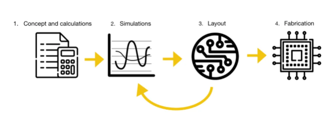
Figure 2.1: Design flow
The design process consists in four sequential steps, from left to right as shown in Fig. 2.1 which are dependent on the previous step and sometimes on the next step, therefore readjustments need to be made, which explains the curved arrow between 3 and 2. The four steps are the following:
1. Concept and calculations: the first step consists in the statement of the concept, this is: what
is going to be built and which characteristics are desirable, for instance power output, FSR, central fre-quency, modulation frefre-quency, etc. This is followed closely by the calculations of BB parameters in each module (laser and IQ), based on structural characteristics and physical properties in order to achieve a certain theoretical result. Calculations result in dimensions of each building block so as to fulfill certain requirements related to power output, spectral characteristics, space limitations and signal shape in the time domain.
2. Simulations: the second step employs a time-frequency electro-optic simulation program which
The simulation program receives the parameters calculated in step one as an input to its custom building blocks and adapts their characteristics to the desired ones in order to achieve a certain functionality. In this step, simulations are carried out on the theoretically calculated modules to ensure their correct operation. Outputs of the simulations include time and frequency results, for instance, transfer functions, output power for certain excitation values, optical spectra, signals in time domain, etc. Popular softwares include VPIphotonics [24], Lumerical [25], Photon Design [26], etc.
3. Layout design: the third step consists in the routing and setting of the electrical connections
required to manufacture the PIC on a multi project wafer. This step is closely related to the second one, as the simulation program employed before allows for the export of optical modules to the layout design software, therefore rendering an easier task to perform the electrical connections with the optical building blocks. For this purpose, a software is employed which includes electrical and optical elements adjustable to a specific purpose. Typical softwares include Synopsys Photonic Solutions Optodesigner [27], Luceda Photonics [28] and Nazca Design [29]. This step is somehow restrictive when it comes to dimensions. The available multi project wafer has fixed dimensions and the layout must follow the manufacturer design rules which determine the separation between optical modules and/or electrical modules. For instance, rules followed in this project include keeping a separation of 250µm between SOAs, 50µm between low bit rate modulation EOPMs, maintaining at least 30µm between waveguide cores, avoid bending deep waveguides with a diameter smaller than 200µm, avoid overlapping electrically driven elements such as electrical routing with photodiodes, EOPMs, SOAs and signatures. There are two kinds of design rules, in the first place the recommended design rules, developed to optimize module efficiency but which are not compulsory, and secondly the mandatory ones, these rules are necessary to ensure the correct performance of the modules, therefore, designs sometimes need to be adjusted to fit these requirements and step two needs to be repeated. This is the reason for the curved arrow in Fig. 2.1.
4. Fabrication: the fourth and last step occurs when the PIC is correctly designed, simulated,
assembled, and electrically routed. It involves sending the design to a specific foundry for its manufacture, which could be SMART Photonics [30] or Fraunhofer HHI [31]. The design can be included in a shared MPW with other users designs which reduces the cost per user, or either the complete run could be dedicated to a single user, remarkably mores costly. In the next section an overview will be given on the software used in each of the four steps as well as some details on the fabrication process.
2.2
Software used and manufacturing
2.2.1
SMART Photonics B.V.
The collaboration between SMART Photonics B.V. and the ETSIT UPM involves a non disclosure agree-ment (NDA), which prevents the detailed description of confidential modules and sections, therefore, certain specific data will not be included in the description of this project.
Foundry:
of semiconductor layers over a crystalline substrate with a well defined orientation [32] and re-growth, processing, polishing and dicing of wafers into chips [21].
The materials employed for the fabrication of the PIC are the following and can be seen in Fig. 2.2:
Passive section: InP negatively and positively doped in blue.
Active section: p-InGaAs and multi-quantum wells (MQW) in red.
Waveguides: passive waveguide material such as Q 1.25 in green.
Back of the wafer: metallized to provide a common ground contact.
Facet coating: anti-reflection dielectric coating, to prevent light reflections into the PIC.
Figure 2.2: SMART Photonics building blocks composition
SMART Process Design Kit (PDK):
SMART Photonics owns a specific PDK, which can be integrated into almost any standard software. It consists of an extensive pre-defined generic building block library and design rules, useful for fast prototyp-ing and accesible to the user. Complex custom designed photonic circuits are designed by interconnectprototyp-ing modules available in the PDK. This PDK may include an automatic design rule check (DRC), which en-sures that design rules are not violated. The design should be then exported to a GDS file employing an appropiate software, sent to the foundry and finally fabricated. The generic modules in the SMART Photonics PDK adapted to VPIphotonics Design Suite (DS) which have been most implemented in this project can be seen in Fig. 2.3. These include from left to right a photodiode to convert an optical signal into an electric current, an EOPM used in phase modulation, a 2×2 coupler, an isolator to protect op-tical modules from external currents and a bent waveguide to interconnect other modules. They will be explained in their respective schematics, recall there are certain confidential properties.
Figure 2.3: Some SMART Photonics PDK BBs in VPIphotonics DS
2.2.2
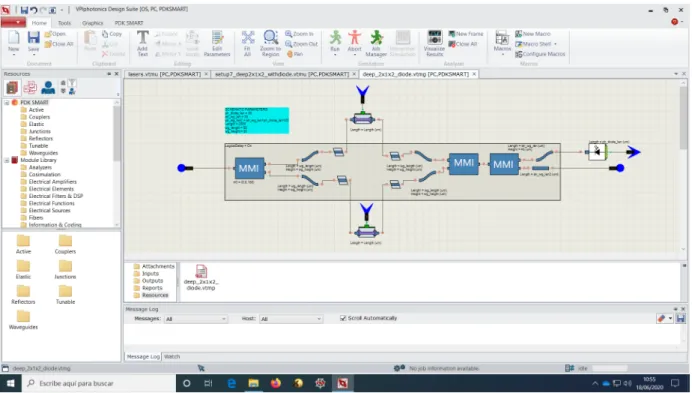
VPIphotonics Design Suite
combine them into larger modules, simulate them, analyze the results and export both the modules and the results to several formats which can be imported into other programs. An interesting feature is that VPI accepts building blocks specific for each foundry, therefore, it offers the possibility to design and simulate modules which can be constructed later in a foundry, for this project the SMART Photonics foundry is accessed. VPIphotonics DS offers a graphic interface for simplicity as can be seen in Fig. 2.4.
Figure 2.4: VPIphotonics DS user interface
1. Simulation methodology:
In VPI Photonics, simulations are the main objective, therefore, simulation parameters are customiz-able. VPI offers two main simulation domains: time domain simulation for active elements and frequency domain simulation for passive elements.
The time domain is more appropriate when working with amplifiers, lasers, etc. It should be activated when an element contains active and/or dynamically tunable components. This domain is sustented on theSample mode, used to pass signals bidirectionally on a sample by sample basis (see Fig. 2.5 (a)). Each sample contains optical field information representing the phase and amplitude of the optical field during a slice of time (in the order of picoseconds or less). This method fires each time one sample is available in the input of the module. For instance, it accounts for lasers with compound cavities, or external reflectors.
Sample mode is the most general form of device and subsystems simulation as it allows almost immediate communication between two adjacent modules, in both directions, which enables modelling optical resonances such as lasers and external resonators that are simulated by combining models of their elemental parts [33].
Figure 2.5: (a) Sample mode (b) Block mode [33]
of ∆s = v∆t, where v is the propagation speed in the simulated medium. The nodes resulting from the spatial discretization are called ”scattering nodes” and considered to be interconnected by lossless transmission lines. This allows the model to perform calculations in each scattering node independently from each other, simply using information from the adjacent nodes in previous itera-tions. Each scattering node contains information about gain (stimulated emission), loss (scattering and absorption), noise (spontaneous emission) and reflections that optical waves experience while passing through the section [33].
The great advantage is that it enables the simulation of compound cavities, multimode lasers, non-linearities, evolution of optic spectra, phenomenons in spectra during modulation (mode-hopping, dynamic chirp, instabilities) and the effects of external optical components, relaxation oscillations, etc.
The frequency domain is less precise and can only be activated when all elements in the setup are passive, however it is considerably quicker. It employs the ”Block mode”, which passes signals uni-directionally. Each block contains a large number of samples (in the order of thousands). In this method optical signals are independently processed by each module, which waits until enough sam-ples are in its input and then fires. Each module is characterized by its scattering matrix in the frequency domain which is applied to all samples in a block.
Both domains can be combined in a hybrid time-and-frequency-domain modeling (TFDM) simulation in which the schematic contains active and passive elements. Passive elements are introduced into a bubble-like-module calledvirtual galaxy, which allows a passive module to adapt its scattering matrix at the same time that nodes in the active elements process samples with their transfer functions.
There are multiple available simulation parameters when performing simulations:
TimeWindowspecifies the duration of the time trace being simulated, which does not mean that
the simulation lasts that duration, it is usually much longer. It also specifies the length of Fourier transforms used in spectral analysis, hence, the frequency resolution in optical spectra is equivalent to its inverse: ∆t= T W1 whereT W is the TimeWindow parameter.
SampleModeBandwidthdetermines the optical bandwidth over which the simulation operates as
determined by:
s= round(L BW ng
c ) (2.1)
where Lis the length of the laser, SOA or resonator,ng is the group velocity andc is the speed of light. These parameters condition the precision of the simulations, therefore, the longer the simu-lations and the higher the sampling rate, the more precise the simusimu-lations result in both domains: time and frequency.
SampleModeCenterFrequency is usually employed in optical circuits and sets the center of the
simulated bandwidth as well as the carrier optical frequency.
GreatestPrimeFactorLimitconditions the number of samples that are generated in a simulation,
to ensure speed of the FFT in the simulations it should be 2, which introduces the condition that the number of samples be a power of 2.
2. Set of building blocks:
The set of available building blocks offered by VPI and by SMART Photonics is large. Those mostly utilized in this project can be seen in Fig. 2.6. These include from left to right: chop signal module
Figure 2.6: VPIphotonics Design Suite recurrent simulation blocks
to remove a certain temporary part of a signal, 2Dimensions analyzer to plot one variable against one parameter, generic analyzer to perform time and frequency analysis, power meter to measure power, sinusoidal generator, DC source, OOK generator to generate a pulsed signal, continuous wave (CW) laser, constant function to access a specific module or simulation parameter, block to sample module to combine passive and active modules in the same schematic and SOA for amplification.
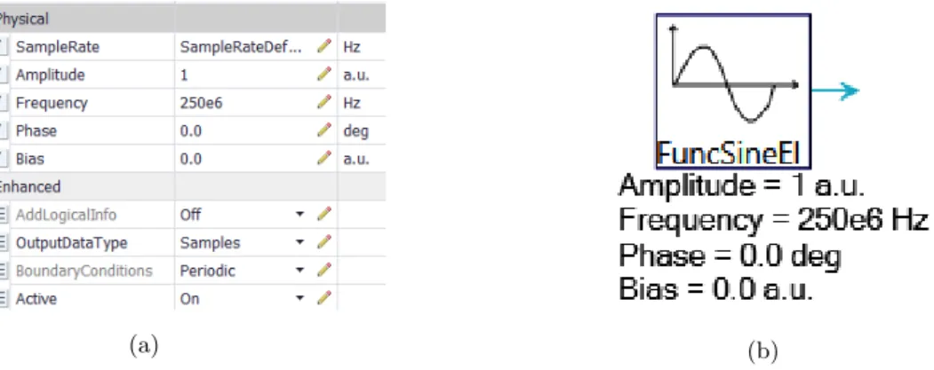
Each building block has certain characteristics (see Fig. 2.7 (a)), which will be explained in detail in the schematics where they are included. Some of them are confidential, property of VPI or SMART, which are explained in a User Manual in order to understand the behaviour of the block but are not accessible, while other characteristics are passed as parameters to the user and can be modified.
An example can be seen in Fig. 2.7 (b), an electrical sine generator in which certain parameters such as length and induced phase shift among others can be modified.
Building blocks can be combined and set into a customizable module called galaxy, which can be comprised into auniverse (see Fig. 2.8 (b)), in which certain parameters can be fixed and others can be externally modified according to the specific purpose. This property is interesting when a combination of building blocks is reutilized, and no modifications need to be made, it allows to simplify complex projects.
3. Results of analysis :
(a) (b)
Figure 2.7: (a) Parameters dialog window (b) VPIphotonics DS sine generator
(a)
(b)
Figure 2.8: (a) Four-section laser galaxy (b) Generic scheme for galaxies and universes
spectrum, electrical spectrum, eye diagram, Poincar´e diagrams, numerical, polarization y constella-tion analysis. In this project only waveform, optical spectrum, eye diagrams and numerical analysis are performed. They are described in the following:
Waveform analysis: a virtual oscilloscope included in VPIphotonics DS is employed. The output
optical or electrical signal is shown in the time domain, power against simulation time is shown (see Fig. 2.9). It is possible to analyze signal phase, chirp, power, as well as include different filters to the signal (Gaussian and low pass filters).
Optical spectrum analysis: an optical spectrum analyzer (OSA) is included. The optical and
electrical spectrum can be viewed and analyzed with this module. Bandwidth can be adjusted and parameters such as phase, group delay, dispersion, etc. are available.
Eye diagram analysis: this analysis are performed using the virtual oscilloscope. They are
ade-quate when exciting a schematic with a digital signal. Available parameters to analyze include BER, Q factor, rise time, bit time, jitter, fall time, etc.
exci-Figure 2.9: VPI waveform analysis
Figure 2.10: VPI optical spectrum analysis
Figure 2.11: VPI eye diagram analysis
tation values. A numerical analysis allows to perform a sweep over a certain parameter and plot the output signal power measured by a power meter, in relation to that parameter.
4. Export data and modules:
Figure 2.12: VPI numerical analysis
2.2.3
Nazca Design
The third step consists in assembling the layout of the chip. For this purpose a Python archive is exported from VPIphotonics DS which contains the optical modules. This file is then imported into Spyder, an open integrated development environment (IDE). Recall that the Python archive only includes the optical module assembled in VPIphotonics DS software, it does not include the layout of the chip design. For this purpose, Nazca Design is employed. Nazca Design is an open source Python library employed in PIC design framework specially interesting for this project as it is compatible with building blocks exported by VPIphotonics and the Process Design Kit (PDK) from certain foundries. It also has available optical and electrical elements as well as additional building blocks to add to the chip, and offers the possibility to export the complete design as a GDS file.
KLayout imports the GDS file, this program is necessary for PIC physical verifications and allows to spot building errors in a visual and easy way. Materials employed are also shown in KLayout (see Fig. 2.13).
(a) (b)
Figure 2.13: Material visualization in KLayout
SMART Photonics is the foundry which will be accessed in this project, it is compatible with Nazca Design and the modules exported from VPI Photonics.
Four section DBR Laser
LASER is an acronym for “light amplification by stimulated emission of radiation”. A laser is a device that emits a beam of coherent light through stimulated emission when excited with an electromagnetic field. Two terms appear that ought to be explained: coherent light and stimulated emission.
The term “coherent light” refers to the set of electromagnetic fields in a beam emitted by a coherent source in which all photons in the light beam travel at the same frequency, direction, polarization and with constant phase difference between them. Coherence can be divided in temporal coherence and spatial coherence, both terms make reference to keeping coherent properties, the first term in a certain space point along a sufficient time interval, and the second term maintains coherent properties in a given instant along a sufficient space area [34]. Coherent beams exhibit certain properties that have been exploited through the years, some of them will be mentioned [35]:
Spatial coherence allows for the transmission of information through long distances in space without increasing divergence.
Temporary coherence permits the emission of a very narrow band spectrum beam.
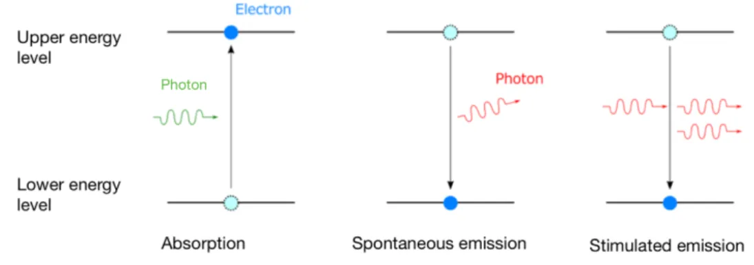
The second term: “stimulated emission” refers to one of the mechanisms that governs light-matter interaction in which lasers are sustained [36].
Figure 3.1: Light-matter interaction mechanisms
is incident on a falling particle and two photons of the same frequency, direction and polarization as the incident one are emitted (see Fig. 3.1) [39]. Stimulated emission is the basic principle of amplifiers and lasers.
Figure 3.2: Stimulated emission physical principle
Lasers are composed of three main ingredients, as can be seen in Fig. 3.2 a resonating cavity, a gain or lasing medium where stimulated emission occurs, and a pump current responsible for population inversion. In order to produce laser emission, a pump current is injected, firstly spontaneous emission occurs when population inversion is achieved, later stimulated emission of photons occurs. Pump current can be either an electrical current or another beam of light of different wavelength than the laser output. Photons then bounce between both reflectors that compose the optical cavity or resonating cavity, notice that the front reflector is partially transparent and allows light to exit the device. With views to controlling beam parameters such as polarization, wavelength, and shape of the beam, other modules can be integrated into the laser.
Lasers can be sorted into three main categories, which appeared gradually through time. Solid-state gases, gas lasers and semiconductor lasers. Solid state lasers appeared in 1960, California, with T. H. Maiman’s first operative ruby laser design chromium doped. The main characteristic that distinguishes them from other lasers is the fact that the gain medium is a host crystal or glass, ion-doped with a rare-earth impurity such as ytterbium or erbium to achieve population inversion [40]. An optical current of higher frequency than the lasing intended is then applied to the lasing or gain medium for stimulated emission to take place, usually from a semiconductor laser or a lamp. Their uses range from welding to surgery and other medical uses.
Parallel to solid-state lasers, in 1960 gas lasers appeared. Ali Javann and W.R. Bennett achieved the first Helium Neon laser. Gas lasers offer important features not available yet in solid state and semicon-ductor lasers, for instance power emission up to hundreds of kilowatts employed in industrial processes and manufacturing. The physical property that sets gas lasers apart from the remaining lasers resides in their atom composition. Instead of continuous energy bands, their energetic structure is composed of discrete levels, which allows for an extremely narrow band emission spectrum.
section, as they will be included in the PIC which results from this project.
3.1
Semiconductor lasers
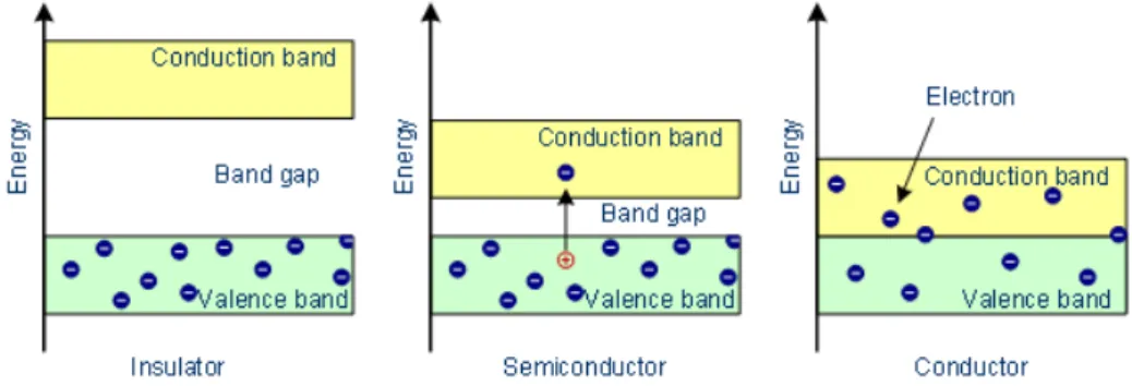
Semiconductors are materials that do not transport electrical current naturally, but electrons are free enough to manipulate them and employ them as light amplifiers or lasers. This occurs because matter is made up of atoms, which are composed of a nucleus formed of neutrons and protons, and outer layers, inhabited by electrons. Bands are filled with a maximum number of electrons, and when a layer is filled, then an outer layer begins to fill. The difference between conductors and insulators is that in conductors, the conduction band is touching the valence band, therefore it is easy for electrons in the valence band to move into the conduction band and carry an electric current. Insulators, on the other hand, show a very high energy gap between both bands, hence, it is not easy for electrons to move and conduce electric current (see Fig. 3.3).
Semiconductor lasers are also known as laser diodes, which implies they are composed by two sections of different electrical properties. Semiconductor lasers are formed by a gain section which is the junction of two or more slightly different semiconductors.
Figure 3.3: Band structure of conductors, semiconductors and insulators
Take Silicon (Si) for instance as the doped material, Silicon hosts four electrons in its outer layer (see Fig. 3.3). One section of the Si semiconductor is doped with an atom such Arsenic (As), which hosts five electrons in its outermost layer, therefore in Arsenic doped Silicon there is one extra electron in the outermost layers (see Fig. 3.4b). However, when Silicon is doped with Boron, which hosts three electrons in its outermost layer, there is one electron missing, known as a “hole”, in the Boron doped Silicon (see Fig. 3.4c) [40].
(a) Silicon without impurities (b) Silicon n-doped
(c) Silicon np-doped
As a result of atomic properties of Silicon, when Arsenic doped Silicon and Boron doped Silicon are placed next to one another and an electric current is pumped through both mediums (see Fig. 3.5), the extra electrons are excited, so when a photon released by spontaneous emission is incident on these electrons, they recombine with the extra holes and a stimulated emission photon is emitted with the same direction, polarization and frequency than the incident photon.
Bear in mind that bands in semiconductors are not discrete as they are in gases, therefore when an electron is recombined with a hole, the energy released is not always the same, thus, the emitted photons do not maintain exactly the frequency of the incident photon according to Plank’s equation, which results in a broadening of the delta-like emission spectrum, which does not occur in gas lasers for instance, as their atoms are composed of discrete levels:
E=hν (3.1)
For this project, the semiconductor laser module must satisfy certain specifications:
1. Small size (order of micrometers): as will be included in a PIC of dimensions 4mm×4.6mm 2. Single mode emission
3. Stable spectrum with changes in temperature and current small fluctuations
4. Output beam should exit the laser horizontally, as light travels parallel to the PIC plane.
5. Tunable to different wavelengths: in order to achieve certain objectives, for instance to be able to support wavelength multiplexing and for its further applications in gas spectroscopy.
Distributed Bragg Reflector (DBR) semiconductor lasers comply with the requirements.
Figure 3.5: Semiconductor laser as a dipole component
3.1.1
Fabry-P´
erot cavity
DBR lasers work following the same principle as Fabry-P´erot (F-P) cavities. A F-P cavity is composed of two semi-translucent reflectors at both ends of an optical cavity. Generally, the rear mirror is high reflectivity and the front mirror is low reflectivity. Light is injected through the rear mirror and is reflected against the front mirror, forming longitudinal modes or standing waves, this process could go on indefinitely should the mirrors be completely opaque, however, as they enjoy a transmission coefficient different than zero, some of the light is transmitted through them.
up given maximum transmission, however, should the standing wave arrive at a mirror in phase opposition then the transmitted rays will cancel each other out [40]. In a wave, the same phase is repeated every travelled wavelength, in the interferometer light travels back and forth between the mirrors, therefore, if the mirrors are separated a distance multiple of half the light wavelength, according to Eq. (3.2) then the reflections that arrive to the rear mirror are in phase with each other but in phase opposition with the incident ray, therefore, behind the F-P there is no transmitted power.
E=mλ
2 (3.2)
Conversely, light reflections reach the front mirror in phase and do not cancel out with any other ray, therefore, all the power will exit through the front mirror. A simple example is given in Fig. 3.6.
Figure 3.6: Fabry-P´erot interferometer [42]
Hence, the spectrum of a Fabry-P´erot is comprised by all the wavelengths that comply with Eq. (3.2), as shown in Fig. 3.7. Notice that the frequency separation between two consecutive modes is known as Free Spectral Range and is only function of the cavity length and cavity refractive index, it does not depend on the mirror reflectivity:
F SR= c
Lef f
(3.3)
Figure 3.7: Fabry-P´erot transmission function [18]
which act as the desired filter. An introduction on them will be given to understand the final laser used in this project.
3.1.2
Bragg gratings
Bragg gratings consist of a segment in which the core has been altered, its refractive index is modified periodically so that a specific wavelength is reflected, and the rest are transmitted.
This creates an optical filter centered in a specific frequency known as “photonic stopband” or “reso-nance frequency” following Bragg’s equation (see Eq. (3.4)) [43].
λB= 2nef fΛ (3.4)
WhereλB is the resonance wavelength or “Bragg wavelength”,nef f refers to the effective index of the optical fiber’s core and Λ represents the pitch length of each periodic segment. Bragg gratings are most commonly employed in optical sensors in construction and fiber optics maintenance, DBR lasers, VCSELS, sampling grating lasers and DBF lasers [44].
Figure 3.8: Bragg grating
Having introduced Fabry-P´erot and Bragg gratings, the explanation of DBR lasers is straightforward. It will be nevertheless explained, as a detailed analysis will have to be performed in order to design the laser in this project’s PIC.
3.1.3
Distributed Bragg reflector lasers
A DBR laser or Distributed Bragg Reflector Laser, is a device increasingly popular due to its easy tuning capacities. It is a component similar to the Fabry-P´erot interferometer in which the optical cavity is built with a n-doped semiconductor and p-doped semiconductor and where the lateral mirrors have been substituted by Bragg gratings (see Fig. 3.9), therefore allowing for single frequency tunability and spectrum stability [15].
Figure 3.9: DBR laser
3.2
Laser design and analysis
Among the most common tunable DBR laser designs there is the four section DBR laser, composed by a front distributed Bragg reflector (DBR), a gain section, a phase controlling section and a rear DBR section, as can be seen in Fig. 3.10:
Figure 3.10: Four section DBR laser
The functions of the front DBR, rear DBR and gain medium have been thoroughly explained in former sections in this project. A brief summary will be given.
Gain section function
The importance of the gain medium consists in the ability to emit photons when an electric current is injected into a semiconductor medium, this is the base of the lasing principle.
DBR sections function
Each DRB act as a partially translucent reflector which allows for photons to bounce between them and stimulate other photons with the same desired frequency, direction and polarization as the previous photons, the front DBR is shorter, therefore the opacity is reduced, in order for the laser beam to exit through the front DBR, while the rear DBR is longer and its opacity is higher. Both DBRs conform a Fabry-P´erot, this allows for a very precise tuning and high efficiency.
Phase section function
Hence, mode hopping occurs. The phase section prevents this mode hopping from occurring by intro-ducing a phase shift in the electric field that travels within the FP cavity [45], this provokes a fine shift in the lasing frequency, as the electric field arrives to the front mirror with a different phase than originally, therefore each mode is frequency shifted, the result is that mode hopping is fixed and all frequencies can be correctly tuned.
3.2.1
Calculated dimensions and parameters
The dimensions of each section are determined in order to establish the working conditions of the four section DBR laser.
Reflective section design: distributed Bragg reflectors (DBR)
Computations on pitch length and effective index are required based on the desired tuned wavelength. Given the desired lasing wavelength of 1550 nm it is possible to calculate the pitch dimensions following Fig. 3.11, which results in 237 nm. Given the expression in Eq. (3.4) where Λ represents the pitch and
Figure 3.11: Bragg wavelength as a function of pitch [46]
λB the tuned wavelength, the effective index nef f can be calculated, which refers to the behavior some heterogeneous materials have when behaving like a homogeneous material. This project’s DBR is composed of two materials of high and low refractivity, however, the DBR as a homogeneous material propagates the waveguide mode as if it had a refractive index of 3.266 [46].
Secondly, a small coupling coefficient is desired in order to avoid reflected fields in both gratings to interfere with each other. It has been fixed by the foundry atk= 50 cm−1. At the Bragg wavelength, the
reflection of a DBR grating is given by:
Lef f =
tanh(kLg)
2k (3.5)
whereLg is the grating length andLef f refers to the effective length.
Gain section design: semiconductor optical amplifier (SOA)
Phase section design: electro optical phase modulator (EOPM)
In this project, the phase section consists in an Electro Optical Phase Modulator (EOPM). This device introduces a phase shift in the travelling electromagnetic wave inside the Fabry-P´erot cavity, the result is that the electromagnetic field reaches the end of the cavity with a different phase, therefore a different frequency is transmitted which allows to avoid or soften mode hopping.
The EOPM available in SMART Photonics PDK introduces a π phase shift when it measures 2mm. An EOPM of 200um has been chosen in this project to introduce a phase shift of 10π rad, equivalent to 18◦. The process of choosing EOPM length has to be very thorough as a longer section is appropriate to reduce mode hopping, however, a shorter section ensures greater FSR and single mode emission.
VPIphotonics Design Suite
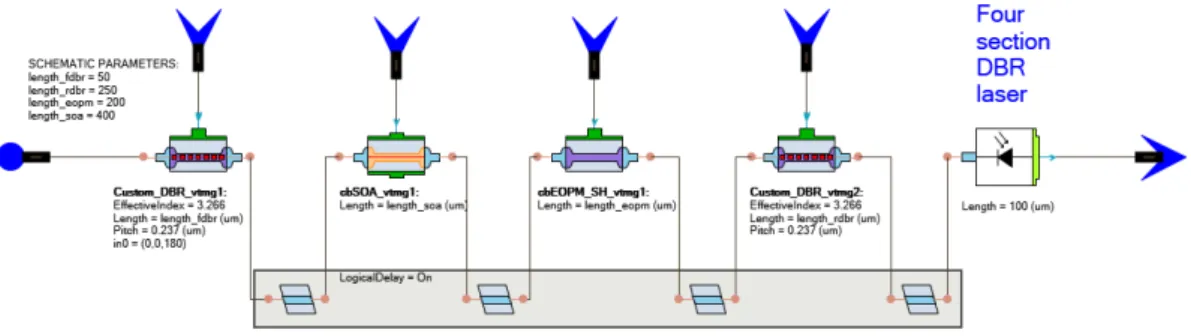
The design and simulations of the laser were performed with VPI Photonics. We used the available modules in VPI that could be later exported to Nazca using the python library of SMART Photonics, which contains the available modules of SMART Photonics (see Fig. 3.12).
Figure 3.12: VPI four section DBR laser design
The components are:
1. Front DBR (FDBR): measures 50 um for a reflectivity of 0.24. Its pitch parameter is 237nm and as a whole, it behaves with effective index of 3.266.
2. SOA: of dimensions 400um to lase with power ranging 20mW.
3. EOPM: measures 200um and introduces a phase shift of 18◦.
4. Rear DBR: its length is 250um [46] which increases its reflectivity to 0.84.
5. Photodiode: this device receives a beam of and produces an electric current. Its responsivity is 0.85 A/W . It will be employed to ensure the laser is emitting power. Its dimensions are of 100µm, which is a usual value according to VPI examples in the VPI platform.
6. Isolators: they prevent electric current leaking into an electrically driven device. SMART Photonics highly recommends placing them in the boundaries of EOPMs and SOAs. Their default length is 30um.
F SR= c
2nef f(LSOA+Lef f,f rontDBR+Lef f,rearDBR+Lphase+NisoLiso)
(3.6)
NAZCA design
When exporting VPI building blocks to Nazca and visualized in KLayout, the result is shown in Fig. 3.13.
Figure 3.13: Nazca laser design
3.3
Laser simulations
In order to characterize and analyze the laser, a generic setup was designed (see Fig. 3.14).
Figure 3.14: Laser measurement setup
The modules involved in the generic setup include the following:
1. DC sources: they provide the injection currents for the internal components of the four-section laser
2. Function analyzers: they are generic modules which enable the user to analyze the output signal of any device in frequency and time domains, this is, the optical spectrum of a signal can be analyzed as well as its power variations in time.
3. Power meter: it is originally designed to measure power in “blocks”, which means that its expected input is the output of a scattering matrix working in the frequency domain.
4. Two-dimension graphs: as their name indicate, they are intended to plot one dimension against the other. In this setup, the plotted variables are power against any other variable that is being studied, in this example the FDBR injection current is being analyzed (see Fig. 3.14).
6. ChopSignal element: this module is compulsory in this setup due to the inclusion of a laser. The output signal of a laser firstly experiences a transitory in which the power is not stabilized (see Fig. 3.15 (a)). Hence, in order to measure a stabilized power value, the ChopSignal module does not measure during a transitory equivalent to the first half of the received signal, in the example 6ns (see Fig. 3.15 (b)).
Figure 3.15: (a) Relaxation oscillations in a semiconductor laser (b) Relaxation oscillations removed by ChopSignal
Figure 3.16: (a) Optical spectrum of a signal experiencing a transitory (b) Optical spectrum of a signal without a transitory
The main advantage of the four section DBR laser is its easy tunability, therefore, in the following sections, wavelength tunability will be analyzed. The following questions will be answered: which is the output power of this laser? in which wavelengths can it be tuned? how is it affected by injection currents into the SOA, front DBR (FDBR) and EOPM? how does the FDBR length affect tunability and output power?
Power - current curves and optical spectrum
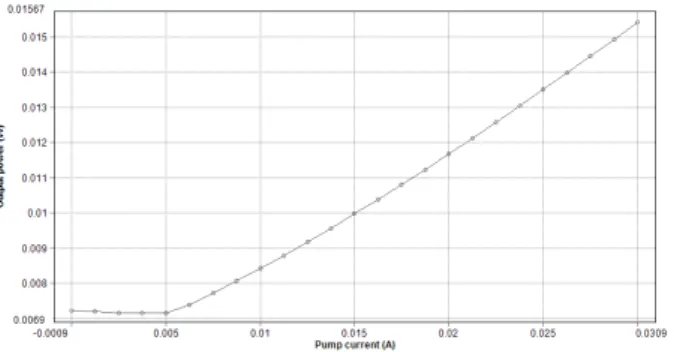
Output power
The main section responsible for power output is the gain section or SOA, therefore, output power is measured when variating the injection current into the SOA. Fig. 3.17 (a) shows that lasers do not lase when excited with a very low injection current, it can easily be seen that a minimum injection current is required to overcome absorption phenomenon in the gain section and other losses. This current is named “threshold current” and its value is 24 mA. It is also appreciable that the maximum output power rounds 40 mW for an input current of 100 mA, therefore, for following simulations, a nominal value of 80 mA will be injected into the SOA to ensure an output power of 27 mW.
(a) (b)
Figure 3.17: (a) Power vs SOA injection current (b) Laser optic spectrum
Power efficiency when lasing at 1550 nm approximately can be determined as the slope parameter of the graph in Fig. 3.17 (a) as Eq. (3.7) indicates, results in 0.526 W/A efficiency.
ef f iciency= ∆P
∆I (3.7)
Optical spectrum
Another fundamental characteristic of a laser is in which wavelength it is emitting. An injection current of 100 mA has been chosen in order to show a well-defined spectrum. Fig. 3.17 (b) shows that this particular laser is working in 1549nm, as it was originally designed to work at 1550 nm, this error of 0.06% is easily assumable.
Wavelength tunability with SOA injection current
Figure 3.18: (a) Wavelength tunability with SOA injection current (b) Color map
optical devices and it is based in the Kramers–Kronig Relations [47], which relate absorption in the gain section with its refractive index for a specific frequency. Following the increase in photo-excitation when SOA injection current increases, absorption in the gain section is reduced, that produces a reduction in the refractive index which is portrayed in lowering the tuning wavelength of the laser [48]. In previous sections, the FSR was calculated and resulted in 0.46nm, Fig. 3.18 supports that argument, as there are exactly 0.46nm between each of the modes.
Wavelength tunability can be analyzed in a parallel way by the employment of color maps, as can be seen in Fig. 3.18 (b). The main advantage of color maps is that each of the optical spectrums emitted for each of the SOA injection currents are shown separately, therefore, they are not overlapped so dependence on injection current is easily shown. The counterpart, however, is that power is not as clearly shown as in traditional power-wavelength graphs.
Wavelength tunability with FDBR injection current
FDBR injection current variation allows for a much finer wavelength tunability than SOA injection cur-rent tunability. The reason for wavelength tunability with FDBR injection curcur-rent is that, in general, the refractive index decreases when the carrier density increases, this produces a shift in the Bragg wave-length towards smaller wavewave-lengths, which reflects its result in reducing the lasing wavewave-length when FDBR injection current is increased [49].
Fig. 3.19 (a) shows the optical spectrum when injecting a 80 mA current into the SOA and variating the FDBR current between values of 0 and 30 mA. Tunability can be also appreciated in the color map in Fig. 3.19 (b).
Wavelength tunability with EOPM injection current
The former tuning methods does not allow whole spectrum tuning. This refers to the impossibility to tune the laser in those frequencies not transmitted by the Fabry-P´erot cavity. In order to avoid or soften mode hopping in wavelength tuning, the phase section is included. Recall that the phase shift included by the 200 um EOPM is 18◦.
Figure 3.19: (a) Wavelength tunability with FDBR injection current (b) Color map
Figure 3.20: (a) Wavelength tunability with EOPM injection current (b) Zoom applied to (a)
In Fig. 3.20 (a) the phase section appears to have little or not effect on the optical spectrum, however, Fig. 3.20 (b) shows that lasing wavelength is slightly shifted, however, even when injecting 30mA, the frequency shift is not enough to compensate mode hopping of 0.46nm. Other techniques should be applied to compensate mode hopping, however, sometimes mode hopping is not a necessarily harmful effect as tuning does not require such great variations.
Dependence on FDBR length
FDBR length is a fundamental parameter when designing the four section DBR laser. Its value directly affects reflectivity, thus providing more reflective mirrors as its length increases. It also directly affects separation between frequency modes, as the FSR becomes smaller as the length increases.
Power measurements
Simulations performed on output power in Fig. 3.21 (a) show two important results.
reflectivity of shorter FDBR results in an increase in the threshold current in order to lase.
(a)
Figure 3.21: (a) PI curves for several FDBR lengths (b) Threshold currents against FDBR length
Secondly, maximum output power is considerably smaller for longer FDBR sections and slope efficiency as well, the reason is the increase of optical losses such as absorption and scattering in longer sections. Another determining factor is the internal series resistance of the DBR, which produces a heat amount and reduces its efficiency. A simple conclusion can be reached: the warmer, the greater the losses which lead to either the greater the threshold current in short FDBR and the lower the efficiency in longer FDBR sections [50].
Optical spectrum
IQ modulator design and analysis
An In-phase and Quadrature (IQ) modulator is able to apply either phase modulation (PM), amplitude modulation (AM) and frequency modulation (FM) to a reference signal. These modulators are employed extensively in digital communications nowadays and offer great security and signal quality. The terms
in-phase andquadrature refer to two sinusoids of the same frequency and which present a 90◦ phase shift between them, by convention the ”in-phase” term is associated to a cosine function and the ”quadrature” term to a sine function. The vector representation of a signal can be seen in Fig. 4.1. I and Q signals
Figure 4.1: Vector representation of a signal
on their own are not particularly interesting, however, when they are added, modulations are achieved. Consider two signals of the same amplitude and phases 0◦ and 90◦, when they are added, the result is a signal of double power and phase 45◦; if amplitude of the I signal is diminished, then the output signal will increase its amplitude and its phase will shift closer to 90◦, hence amplitude modulation and phase modulation are achieved. If phase of the IQ signals vary constantly, then FM modulation is achieved according to the following expression which indicates that instantaneous frequency is a result of phase derivation.
fi= 1 2π
dΦ(t)
dt (4.1)
IQ modulators are generally employed in digital communications to perform a specific kind of phase mod-ulation known as phase shift keying (PSK), this enables a higher spectral efficiency, which means that a higher bitrate can be transmitted in the same bandwidth. In digital communications a finite number of signals is used to represent binary data, PSK modulation assigns a specific phase to each pattern of bits in order to differenciate them from each other. This project will study quaternary PSK (QPSK), in which four phases are assigned to four symbols where each symbol consists of two bits. The modulation scheme and their standard representation can be seen in Fig. 4.2 [51].

![Figure 3.7: Fabry-P´ erot transmission function [18]](https://thumb-us.123doks.com/thumbv2/123dok_es/6858946.838456/31.892.298.647.711.993/figure-fabry-p-erot-transmission-function.webp)