ULTRA-BROADBAND DIRECTIONAL COUPLERS USING MICROSTRIP WITH DIELECTRIC OVERLAY IN MILLIMETER-WAVE BAND
A. M. Pel´aez-P´erez1, *, P. Almorox-Gonz´alez1, J. I. Alonso1, and J. Gonz´alez-Mart´ın2
1Departamento de Se˜nales, Sistemas y Radiocomunicaciones, Univer-sidad Polit´ecnica de Madrid, Ciudad Universitaria s/n, Madrid 28040, Spain
2Altaix Electr´onica, C/Colquido 6, Las Rozas 28230, Spain
Abstract—Nowadays, millimeter-wave systems are being a key factor to develop wide band applications. In this paper, a directional coupler in millimeter-wave band using dielectric overlay is presented. This leads us to technology aspects, in directional coupler design, are key points to achieve the proper response of the circuit. The coupler proposed in this paper covers the 15–45 GHz band and its response has 15-dB coupling-level, 1-dB coupling-ripple and a reflection coefficient better than 10 dB.
1. INTRODUCTION
In the last years, there has been a great interest in the development of radiocommunications systems in upper frequencies, higher than 30 GHz. The main reason of using these high frequencies is due to the demand of warfare systems, and also the appearance of new and emerging applications, which leads to the development of circuits and subsystems in these bands. There are many applications working in millimeter-wave band, as High-Resolution Radars (HRR) in the area of electronic warfare or LMDS and WiMAX systems in the area of communications [1].
Moreover, using the higher part of the spectrum makes possible increasing the available bandwidth, reducing the interferences with other systems and services, minimizing the size of circuits, and the use of a less saturated spectrum [2–6]. However, the main problem
is solving the new technological problems that appear in these high frequencies, besides the design, assembly and manufacturing of circuits and systems in these bands.
Directional couplers are key circuits used in many microwave and millimeter subsystems [7]. Their function involves acquiring samples of the input signal. The design, development and measurement of an ultra-broadband directional coupler using microstrip technology with dielectric overlay are presented in this article. Moreover, the main problems of developing this kind of circuits in millimeter frequencies are described and solved.
The developed coupler bandwidth is 1.585 octaves, from 15 GHz to 45 GHz. The obtained results show good agreement with the simulations and the coupler shows a good performance in the whole bandwidth.
Section 2 describes the basic theory of the design techniques. Section 3 presents the designed directional coupler. And, in Section 4, the simulations and measurements of the circuit designed are compared. Finally, the main conclusions of this work will be presented in Section 5.
2. DIRECTIONAL COUPLERS USING MICROSTRIP WITH DIELECTRIC OVERLAY
Multi-section directional couplers consist of severalλ/4-length coupled transmission lines sections connected in cascade. These circuits have a flat behavior in the coupling response in a relatively wide band, and also a good performance in the return losses and isolation responses.
The main problem of this kind of circuits is their development in microstrip technology, because of the directivity is reduced as there is a certain difference in the phase velocities of the odd- and even-modes in a non-homogeneous material. Solving this problem is a crucial factor, since this technology is used in many radiofrequency systems as it allows obtaining compact circuits with low cost. Another alternative in order to design wideband directional couplers at microwave frequencies is the use of buried homogeneous structures [8], as multilayer LTCC technology, since this kind of structures support TEM modes with the same phase velocity. However, LTCC technology supposes a high cost due to process fabrication complexity and materials prices, so it is more suitable for mass production, while conventional microstrip technology is simpler and cost-effective.
or sawtooth [9], using anisotropic substrates [10], or using dielectric overlay [11–14]. The last technique has been selected in this article because it has been considered the more suitable to work at the high frequencies of millimeter-wave band.
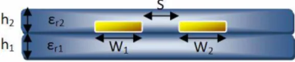
The use of dielectric overlay makes the phase velocities of both modes equals since there is an increase in the effective dielectric constant of the odd-mode and a decrease for the even-mode. Thus, the presence of overlay means a reduction in wide and gap of coupled lines for a constant value of odd- and even-mode impedances. Figure 1 shows the scheme of a pair of coupled lines with dielectric overlay.
Figure 1. Coupled lines with dielectric overlay scheme.
There are several techniques to analyze and characterize coupled-lines in microstrip technology with dielectric overlay, for instance, the empiric method based on changes in the obtained data from coupled-lines in microstrip technology without overlay [12], or the numeric method proposed by Sheleg and Spielman [13]. Another technique is the one proposed by Paolino using the spectral domain [14].
The technique in [12] consists in designing couplers in microstrip technology with overlay from the tables for couplers without overlay proposed by Levy in [15]. In these tables, the odd- and even-impedances of each coupler section are calculated as a function of the coupling level, the number of sections, the bandwidth and the coupling ripple. And then, the physical dimensions of every pair of coupled lines are obtained from the odd- and even-impedances. In the case of couplers with overlay, the final dimensions of every section are calculated through a series of approximations based on empirical changes in the data of the coupler without overlay.
On the other hand, in [14], a technique in the spectral domain is used to analyze a coupled line with overlay which allows obtaining the Green’s function to study this kind of coupled structure.
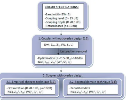
3. DESIGN OF AN ULTRA-BROADBAND DIRECTIONAL COUPLER
from 15 GHz to 45 GHz (1.585 octaves), 15-dB coupling level, 1-dB coupling-ripple and return losses better than 10 dB. The substrate is Alumina, with 9.9 dielectric constant and 0.254-mm thickness and it has also been used the same substrate for the dielectric overlay.
Herein, the design techniques [12] and [14] are compared and evaluated in the millimeter-wave band circuit design framework. Thus, two directional couplers using dielectric overlay will be designed for both techniques from the same specifications.
3.1. Empirical Changes Technique
For the technique proposed in [12], the first step is to calculate the odd- and even-impedances of every section from the tables for couplers without overlay proposed by Levy [15]. These tables are tabulated as a function of the coupling level, the number of sections, the bandwidth and the coupling ripple.
When it comes to decide which design is the most suitable for the initial specifications, it must be taken into account there are some designs that could not be carried out because too long gaps could be between two consecutive sections depending on the substrate. These long-gaps would involve a transition to connect two consecutive sections, and therefore the response would be significantly worst. Indeed, as the ripple decreases, the difference in odd- and even-impedances increases and the gap between two coupled-lines also increases. Hence, the ripple will be a key parameter in a design that fulfills the specifications and involves not too long gaps between the coupled-lines.
From the tables in [15] (directional couplers without overlay), the feasible design with the minimum ripple for the selected substrate has been established. The resulting design has four sections, 0.487-dB ripple and BW = 8.0 bandwidth. Despite of, there are some designs from the tables in [15] that fulfill the requirements of ripple and bandwidth, the physical implementation would lead to gaps too
Table 1. Odd- and even-impedances for coupled-lines sections using the empirical changes technique [12].
BW =f2/f1 Ripple (dB) Number of section Zo (Ω) Ze (Ω)
8 0.487
1 37.24 67.14
2 41.76 59.86
3 45.41 55.06
long in the coupled-lines, so the design would not be feasible. The odd- and even-impedances for each coupled-lines section are presented in Table 1.
It is simple to calculate the coupled-lines physical dimensions of every section of the directional coupler without dielectric overlay from the odd- and even-impedances. It has been used Linecalc tool from theAdvanced Design System (ADS) software to calculate the physical dimensions using the MCLIN component. These dimensions are shown in Table 2.
The coupler last section has a too much long gap, so its coupling level will be very weak and its influence in the total response of the coupler will not be significant. Thus, it has been decided to remove the last section in order to avoid the long discontinuity between sections and not getting a bad response. This fact is important in high-frequencies where small discontinuities could involve degradation in the circuit response. Once the fourth section has been removed, an optimization of the width and gap of every section coupled-lines has been made using ADS in order to achieve coupling and return losses specifications. The new three-section design fulfills the specifications, whereas a theoretical three-section design from the tables in [15] would perform a 0.99-dB ripple for the same bandwidth, which is twice as much as the four-section design restructured in three-section. The optimized physical dimensions of the directional coupler without dielectric overlay can be shown in Table 3.
Table 2. Physical dimensions of directional coupler without dielectric overlay using the empirical changes technique [12].
BW =f2/f1 Ripple (dB) Number of section W (µm) S (µm) L(µm)
8 0.487
1 201 121 981
2 221 233 963
3 228 427 953
4 229 832 950
Table 3. Optimized physical dimensions of directional coupler without dielectric overlay using the empirical changes technique [12].
Number of section W (µm) S (µm) L(µm)
1 195 123 981
2 229 243 963
Table 4. Physical dimensions of directional coupler with dielectric overlay using the empirical changes technique [12].
Number of section W (µm) S (µm) L(µm)
1 195 123 981
2 229 253 963
3 228 496 953
Table 5. Physical dimensions of directional coupler with dielectric overlay using the spectral domain technique [14].
Number of section W (µm) S (µm) L(µm)
1 140 153 981
2 152 280 963
3 160 470 953
Once the physical dimensions of the directional coupler without dielectric overlay have been obtained, it is time to calculate the final dimensions of the three-section directional coupler with dielectric overlay that can be shown in Table 4. A new optimization process has been executed from the data of the coupler without dielectric overlay in order to fulfill the original specifications.
3.2. Spectral Domain Technique
The second directional coupler presented in this article has been designed with the technique proposed in [14], where a spectral domain technique is used to obtain the Green’s functions which allow the study of this kind of couplers.
From the odd- and even-impedances corresponding to microstrip lines in Table 3, the physical dimensions of every coupled-line are calculated using the technique in [14], where by means of the computation of the Green’s function, the physical dimensions of this kind of coupled-lines are tabulated. These dimensions are presented in Table 5.
Figure 2. Design process of the directional coupler with dielectric overlay for both techniques.
(a) (b)
Figure 3. Asymmetric couplers layout. (a) Design with technique [12]. (b) Design with technique [14].
3.3. Directional Coupler Design Process
ADS to improve the final response of the directional couplers. Both final layouts are presented in Figure 3.
Discontinuities and bend-lines can lead to degradation in circuit response in millimeter-wave band, so discontinuities have been designed to be as smooth as possible and bends have been performed with the 90-degrees matched bend.
It can be seen in Figure 3 that the isolated port is loaded with a 50 Ω broadband load which has been designed as a π-attenuator in order to obtain a good performance in return losses. This attenuator has been designed with printed resistors, as it is not possible to use chip resistors in these frequencies to perform a broadband load. Printed resistors are obtained by depositing a layer of certain material over the
Figure 4. Simulated insertion losses.
substrate, and their value depend on the resistivity and thickness of the material, and the size of the resistor [16]. 50 Ω/square resistors will be used in the manufacturing process as it is the most common value.
4. SIMULATIONS AND MEASUREMENTS
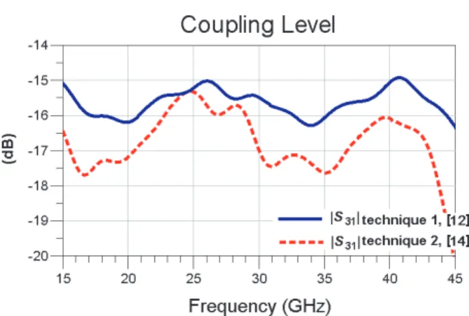
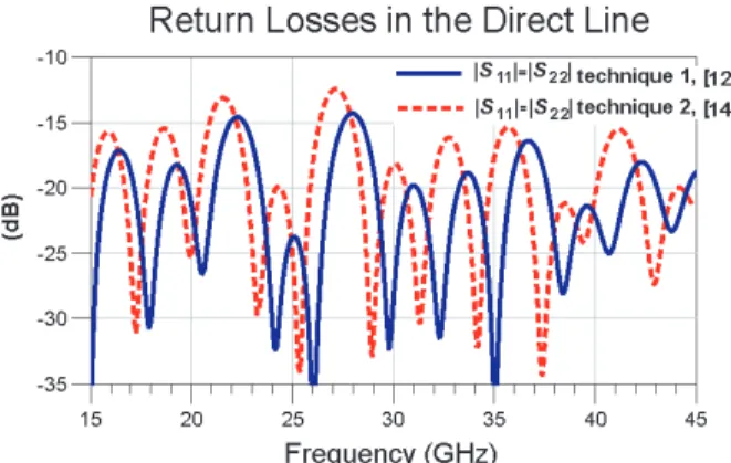
Figure 3 circuits have been simulated using Momentum tool of ADS. Figures 4, 5, 6 and 7 show the response comparison for both designed directional couplers with dielectric overlay.
From these figures, it is shown that the directional coupler designed with the empirical changes technique (technique 1, [12]) has better performance than the directional coupler designed with the
Figure 6. Simulated return losses in the direct line.
spectral domain technique (technique 2, [14]) in the whole bandwidth. The main difference in both responses can be appreciated in the coupling level: 1-dB peak-to-peak ripple fortechnique 1, whereas it is 2.5-dB fortechnique 2. It can be due to the shape of the coupled line, which is thinner in technique 2 and could lead to worst performance in high-frequencies.
Therefore, the directional coupler designed with the empirical changes technique was manufactured byIndra Sistemas S.A.. Figure 8 shows a view of this coupler.
The connectors that have been chosen in this project are the model 1414-06SF 2.4 mm which are manufactured by Southwest Microwave [17] and have an operating range up to 50 GHz. The connectors’ assembly performance has to be done carefully in order to get the best performance. An equivalent circuit and a characterization
Figure 8. View of the designed directional coupler without dielectric overlay for visibility reasons.
Insertion Losses
of these connectors were presented in [16]. Despite this, problems have been detected in the assembly process as it is non-repetitive. This lack of repetitiveness can degrade the connector performance.
The coupler was made using the same type of 0.254-mm thickness Alumina for both the circuit and the overlay. Both have the same outline except at the input and output, where the overlay has been recessed in order to let the line exposed and allow the connections to be made. Both parts were cut by means of a laser. The Alumina with the circuit lines was glued to the bottom of the box using a conductive epoxy.
The circuit was initially measured just placing the overlay on top of the circuit. The overlay was then glued to the circuit using a cyanoacrylate adhesive applied on areas separated from the coupled
Direct Line Phase
Figure 10. Direct line phase of the designed coupler.
Coupling Level
lines, to avoid the glue acting as an additional dielectric layer, thus changing the results. Both results, before and after applying the adhesive, were identical.
The connector pins were connected to the tracks by means of a short gold ribbon.
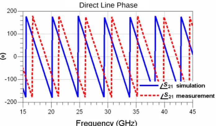
The vector network analyzer PNA E8364A and the 85056K calibration kit, both fromAgilent Technologies and with an operating range up to 50 GHz, have been used to measure the designed coupler. Figures 9, 10, 11, 12, 13 and 14 show the comparison between simulated and measured responses.
The measured response is similar to the simulated one. Level and ripple coupling response match in the whole bandwidth, apart from the band 15–20 GHz where the ripple increases slightly. Measured phase
Coupled Line Phase
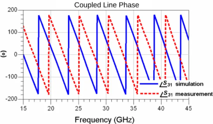
Figure 12. Coupled line phase of the designed coupler.
Return Losses in the Direct Line
Return Losses in the Coupled Line
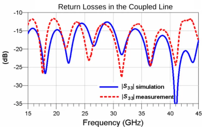
Figure 14. Return losses in the coupled line of the designed coupler.
responses of direct and coupled lines are similar to the simulated ones, their slopes are equal and the gap phase is due to initial frequency of performed simulations and measurements (15 GHz for simulations and 1 GHz for measurements). Return losses in direct and coupling lines are better than 10 dB in the whole bandwidth, despite a small degradation in the measured response, which can be due to a possible mismatch in the connectors. As conclusion, the coupler described in this paper presents a good performance in the whole design bandwidth and it can be integrated in millimeter-wave band subsystems.
5. CONCLUSIONS
The design, manufacture and measurement of an ultra-broadband directional coupler using dielectric overlay in millimeter-wave band have been accomplished. The main problems of developing this kind of circuits in millimeter frequencies have been presented and solved. Two different techniques to design directional couplers with dielectric overlay in this band have been analyzed and compared. The designed coupler presents a good performance in an ultra-broad band, 15– 45 GHz, and fulfills the design specifications.
ACKNOWLEDGMENT
REFERENCES
1. Andrisano, O., V. Tralli, and R. Verdone, “Millimeter waves for short-range multimedia communication systems,” Proceedings of the IEEE, Vol. 86, No. 7, 1383–1401, 1998.
2. Bakhtafrooz, A., A. Borji, D. Busuioc, and S. Safavi-Naeini, “Novel two-layer millimeter-wave slot array antennas based on substrate integrated waveguides,” Progress In Electromagnetics Research, Vol. 109, 475–491, 2010.
3. Wang, Z., B. Zhao, Q. Lai, H. Zhong, R.-M. Xu, and W. Lin, “Design of novel millimeter-wave wideband bandpass filter based on three-line microstrip structure,” Journal of Electromagnetic Waves and Applications, Vol. 24, No. 5–6, 671–680, 2010.
4. Wang, Z., Q. Lai, R.-M. Xu, B. Yan, W. Lin, and Y. Guo, “A millimeter-wave ultra-wideband four-way switch filter module based on novel three-line microstrip structure band-pass filters,” Progress In Electromagnetics Research, Vol. 94, 297–309, 2009. 5. Yang, X.-D., Y.-S. Li, and C.-Y. Liu, “A toothbrush-shaped
patch antenna for millimeter-wave communication,” Journal of Electromagnetic Waves and Applications, Vol. 23, No. 1, 31–37, 2009.
6. Hung, C.-Y., M.-H. Weng, R.-Y. Yang, and H.-W. Wu, “Design of a compact CMOS bandpass filter for passive millimeter-wave imaging system application,” Journal of Electromagnetic Waves and Applications, Vol. 23, No. 17–18, 2323–2330, 2009.
7. Zhang, Q.-L. and S. N. Khan, “Compact broadside coupled directional coupler based on coplanar CRLH waveguides,”Journal of Electromagnetic Waves and Applications, Vol. 23, No. 2–3, 267– 277, 2009.
8. Lopez-Berrocal, B., J. de-Oliva-Rubio, E. Marquez-Segura, A. Moscoso-Martir, I. Molina-Fernandez, and P. Uhlig, “High performance 1.8–18 GHz 10-dB low temperature co-fired ceramic directional coupler,” Progress In Electromagnetics Research, Vol. 104, 99–112, 2010.
9. Podell, A., “A high directivity microstrip coupler technique,” G-MTT 1970 International Microwave Symposium, 33–36, May 11– 14, 1970.
10. Kobayashi, M. and R. Terakado, “Method for equalizing phase velocities of coupled microstrip lines by using anisotropic substrate,” IEEE Transactions on Microwave Theory and Techniques, Vol. 28, No. 7, 719–722, Jul. 1980.
microstrip,”MTT-S International Microwave Symposium Digest, Vol. 82, No. 1, 410–412, Jun. 15–17, 1982.
12. Spielman, B. E., “The development of a 20 dB directional coupler for MIC applications,” MTT-G International Microwave Symposium Digest, 186–188, Jun. 4–6, 1973.
13. Sheleg, B. and B. E. Spielman, “Broad band directional couplers using microstrip with dielectric overlays,” IEEE Transactions on Microwave Theory and Techniques, Vol. 22, No. 12, 1216–1219, Dec. 1974.
14. Paolino, D. D., “MIC overlay coupler design using spectral domain techniques,” IEEE Transactions on Microwave Theory and Techniques, Vol. 26, No. 9, 646–649, Sep. 1978.
15. Levy, R., “Tables for asymmetric multi-element coupled-transmission-line directional couplers,” IEEE Transactions on Microwave Theory and Techniques, Vol. 12, No. 3, 275–279, May 1964.
16. Pel´aez-P´erez, A. M., J. I. Alonso, P. Almorox-Gonz´alez, and J. Gonz´alez-Mart´ın, “Ultrabroadband Wilkinson power divider in millimeter-wave band,” Microwave Journal, Vol. 52, No. 11, 32– 42, Nov. 2009.
![Table 2. Physical dimensions of directional coupler without dielectric overlay using the empirical changes technique [12].](https://thumb-us.123doks.com/thumbv2/123dok_es/6778238.831268/5.681.103.588.630.734/physical-dimensions-directional-coupler-dielectric-overlay-empirical-technique.webp)
![Table 4. Physical dimensions of directional coupler with dielectric overlay using the empirical changes technique [12].](https://thumb-us.123doks.com/thumbv2/123dok_es/6778238.831268/6.681.183.505.182.274/physical-dimensions-directional-coupler-dielectric-overlay-empirical-technique.webp)