XPS AS CHARACTERIZATION TOOL FOR PV: FROM THE SUBSTRATE TO
COMPLETE lll-V MULTIJUNCTION SOLAR CELLS
M. Gabás , M.C. López-Escalante , C. Algora , I. Rey-Stolle , E. Barrigón , I. García , B. Galiana ' , S. Palanco , S. Bijani1 and J.R. Ramos-Barrado1.
1Dpto. de Física Aplicada I, Lab. de Materiales y Superficies, Universidad de Málaga, 29071 Málaga, Spain. i n s t i t u t o de Energía Solar-Universidad Politécnica de Madrid, Avda. Complutense 30, 28040 Madrid, Spain. 3Present address: Instituto de Ciencia de Materiales de Madrid, CSIC, Sor Juana Inés de la Cruz 3, 28049-Madrid, Spain
ABSTRACT
This contribution aims to ¡Ilústrate the potential of the X-ray photoelectron spectroscopy (XPS) technique as a tool to analyze different parts of a solar cell (surface state, heterointerfaces, profile composition of ohmic contacts, etc). Here, the analysis is specifically applied to lll-V multijunction solar cells used in concentrator systems. The information provided from such XPS analysis has helped to understand the physico-chemical nature of these surfaces and interfaces, and thus has guided the technological process in order to improve the solar cell performance.
INTRODUCTION
XPS is a widely extended surface analysis technique; it yields information on the first few nanometers of the film. Their abilities range from the identification of any contaminant or residues at the sample surface to the analysis of the orientation of adsorbed molecules or clusters into a particular surface. Photoelectron Spectroscopy (PES) of core levéis is a sensitive probé of the local chemical environment around the emitting atom. When used in combination with Ar+ sputtering, it can constitute a first approximation to the interface chemistry between two layers, although the effects on the sample surface due to the Ar+ sputtering process (preferred sputtering, metal reduction and Ar implantation) have to be taken into account. Angle resolved XPS (ARXPS) of both, core levéis and Auger transitions among them offers valuable information on the evolution of the oxidation state of a particular catión.
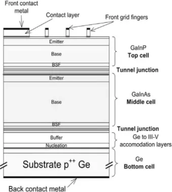
The interface between two layers is a critical part in any layered electronic device, since existing defects and impurities can profoundly affect the final device performance. XPS analysis can detect the formation of spurious compounds that may intensely affect the charge carrier displacement through the interface [1]. Thus, a careful look on the surfaces and interfaces appears as a first unavoidable step to achieve a complete characterization of the whole device. This analysis is especially important in the case of lll-V multijunction solar cells which are made up at least by 30 different layers, of more than 6 different semiconductors, with thicknesses varying from 20 nm to 2 microns and with doping levéis going from 1017 to 1020 cm"3 (see figure 1). Every surface and interface in this layered structure is a potential object of analysis using XPS techniques. Besides, a key task in
these cells is the optimization of the heteroepitaxial growth of lll-V layers on the germanium substrate. It requires that lll-V epilayers on Ge provide a defect-free témplate f o r t h e subsequent epitaxial growth, which in fact is very dependent on the surface state of the Ge substrates.
Front contact metal
Contact I ayer
5*
Front grid fingers
Emilter Base
Emilter
BSF"
BuffEr Nucleation
Substrate p
++Ge
7~~
,
GalnPTop cell Tunneljunction
GainAs Middle cell
}
Tunnel junction G e t o l l W accomodation layers
1
GeBottom cell
Back contact metal'
Figure 1 : Schematic view of a lll-V multijunction solar cell structure. Every layer is a different lll-V semiconductor compound doped with the appropriate element. Red lines represent the three structure levéis we have dealt with in this work.
ANALYSIS AT THE SUBSTRATE LEVEL conclusions relative to the differences in the Ge oxidation state.
A good epitaxy starts with a thorough understanding of the substrate surface. The presence of oxides, contaminants or adsorbates can have a key role in the formation of defects during the subsequent lll-V layer growth [2]. Now we present the study carried out on the surface state of commercial epi-ready Ge wafers from two different vendors, namely wafer A and B. Irrespective of the vendor, XPS analysis shows that all the Ge wafers have an oxide layer and reveáis the presence of carbón and, probably chlorine, although the last element seems to appear in a very little quantity. In wafers A, carbón is present in the form of carbonates and there are some indications that traces of potassium, through the K2p core level signal, could appear cióse to the C1s signal, but the confirmation of its presence needs further experimental work. There are no traces of other contaminants, such as fluorine, sodium or nitrogen in any of the wafers.
1226 1224 1222 1220 1218 1216 1214
BE(eV)
Figure 2: Ge2p spectra of two different Ge wafers, showing the three contributions: metallic Ge, GeO and Ge02 in different proportions.
The very different shape of the Ge core level peaks inform us that the mean oxidation state of the Ge element is not the same in these two wafers, being wafers B much more oxidized. The differences in the Ge mean oxidation state are presented in figure 2, where the Ge2p spectra from two different wafers, namely A and B, are depicted. Three components constitute the core level signal in both cases: metallic Ge, GeO and Ge02, although their relative intensities differ from one wafer to another. No other sub-oxides have been detected. As it is evident in this figure, the related weight of oxidized Ge is larger in wafers B, which implies a thicker oxide layer on these wafer surfaces. Ge 3d core level signáis (not shown) allow to perform the same analysis and to reach identical
01s spectra also evidence the different mean oxidation state of Ge wafers coming from different vendors (see Fig. 3). Two contributions coming from GeO and Ge02, appear in all the wafers. Exactly as it happens for the Ge core level spectra, the deconvolution of the total 01 s XPS signal among their components yields a ratio Ge02/GeO bigger for the wafers B. Moreover, in the wafers where the presence of carbonates has been detected in the C1s spectrum -wafers coming from vendor A-, there is an extra contribution to the 01s core level signal in the high binding energy región (see Fig. 3 top), which does not appear in any of the 01 s and C1s core level spectra from wafers B. There is no other contribution from any other C-0 compound in none of the wafers.
—i ' 1 • 1 ' 1 • 1—
536 534 532 530 528
BE(eV)
Figure 3: 01s spectra of the same two wafers as in figure 2, showing their contributions with different relative intensities.
ANALYSIS OF THE SEMICONDUCTOR STRUCTURE
As an example of the various applications that XPS techniques allow to tackle, we present in this section the study of the oxidation of GaAs and GalnP layers when they are grown onto GalnP and GaAs templates respectively, by Metal Organic Vapor Phase Epitaxy (MOVPE). ARXPS has been used for this purpose. The basis of this technique is that photoelectrons getting out from the sample with different take-off angles respect to the surface layer, provide information from different depths in the film, taking into account that the photoelectrons mean free path is only dependent on both matrix effects and photoelectron kinetic energy. Thus, data taken at small take-off angles supply information of the very first layers.
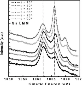
Figure 4: Ga LMM spectra at different take-off angles, probing the Ga oxidation state at different depths in the GaAs layer. Small angles correspond to more superficial layers.
The surface Ga oxidation state in a GaAs layer deposited onto a GalnP témplate has been examinated through the evolution of the Ga LMM Auger spectrum with probing depth. Figure 4 shows these depth-dependent spectra, with a dominant peak centered at ~1062 eV for small take-off angles while for take-take-off angles cióse to 90°, the dominant peak is centered at -1066 eV. The corrected Auger parameter corresponding to these energies are 1082.74 eV (Ga203) and 1085.6 eV (GaAs). Therefore,
from the data shown in figure 4, it can be deduced that the GaAs surface presents a superficial oxide layer, but its thickness is small, (less than 2 nm). On the other hand, the corrected Auger parameter corresponding to As
maintains a rather constant valué between 1266.2 eV and 1266.5 eV, which are typical valúes of GaAs compound, indicating that the As oxidation is almost negligible in the GaAs layer.
On the contrary, when the GalnP layer is grown onto a GaAs layer, the Ga LMM Auger spectra shows that the presence of Ga oxide is almost negligible at the surface of the layer as it has been previously reported by the authors [3]. Therefore, Ga catión is oxidized more easily when exposed to air in the GaAs lattice than in the GalnP compound. Arsenic core level signáis are also detected at the GalnP surface, showing up the possible As segregation from the interface trough the GalnP layer.
Another fundamental probiem in lll-V solar cells is the cross-diffusion of different atoms at the various interfaces in the structure. The interfaces between two lll-V semiconductors have received so much attention because of their fundamental role on the performance of the solar cell device. In that way, the in-depth resolution that XPS can supply is of great relevance in order to determine the abruptness of a heterojunction. Accordingly, a first approximation to the interface GaAs/GalnP has been made by using XPS combined with Ar+ sputter depth
profiling. However, several unintended effects could accompany this technique and must be taken into account.
Approximate depth (nm)
Figure 5: XPS depth profile of the GaAs/GalnP heterointerface.
than that of the Ga (271.72 kJ-mol ). As it is shown in figure 5, the interface is characterized by a strong decay in the Ga and As atomic concentrations, which is indicative of a rather abrupt interface. This decrease of Ga and As signáis is accompanied by the appearance of the In and P core level signáis. The great diferrence in stoichiometry also measured for the GalnP layer (expected to be
Gao.5lno.5P) can be also explained analogously in terms of preferential sputtering of the some of the species in the alloy.
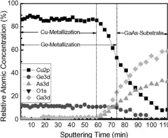
copper oxides and carbón disappear [6]. After the superficial contamination has been eliminated, only Cu and Ge appear in XPS spectrum, showing a metallic layer without any trace of Ge oxides. A continuous Ar+
sputtering process accompanied by XPS analysis of the Cu2p, Ge3d, 01 s, As3p and Ga3d signáis allows to confirm the formation of a metallic Cu/Ge alloy with a homogeneous composition of Cu and Ge, as it is evident from the fíat signal intensity vs. time signal for both elements (see Fig. 6).
ANALYSIS AT THE DEVICE LEVEL
A great deal of attention and effort has been directed towards the achievement of high quality ohmic contacts to GaAs films and other lll-V semiconductors in order to diminish the solar cell series resistance. In the case of concentrator solar cells, these requirements are especially important because the ohmic contact must exhibit simultaneously a low metal sheet resistance and a low specific contact resistance [4, 5]. Cu/Ge alloys could be a good alternative due to their electrical characteristics and low cost as compared to conventional gold or silver-based alloys.
100
10 20 30 40 50 60 70 80 90 100 110 Sputtering Time (min)
Figure 6: XPS depth profile of the layer Cu/Ge and its interface with the GaAs layer.
In order to study the interface between Cu/Ge and GaAs layers, XPS measurements combined with Ar+ sputtering
have been conducted. Epitaxially grown n-GaAs layers were coated with a Cu/Ge alloy (800nm thick) prepared by sequential thermal evaporation of a Cu layer (500nm thick) followed by a Ge layer (300nm thick). A subsequent annealing process at high temperature formed the ohmic contact as well as the Cu/Ge alloy. Before any cleaning procedure, XPS results show that at the topmost of the surface only Cu, O and C signáis are detected. Cu is oxidized at the surface of the layer, but just 1 minute of sputtering with Ar+ ions is enough to make both, the
When the interface with the GaAs layer is reached, the Ge3d core level maintains a constant signal up to a greater depth than Cu2p does. In this región, As and Ga core levéis can also be detected. It seems that a mixture based on Ge and Cu, together with Ga and As has been formed. This layer could be the responsible for the low specific contact resistance reported and thus, for the good performance of the Cu/Ge alloy as ohmic contact [7]. There is no indication of the formation of phases like GeAs2 at the interface. The evolution of the Ge3d, Cu2p core level binding energies and corrected Auger parameters for both elements (see fig. 7) are only compatible with metallic Ge and Cu. This information has been crucial for us in order to optimize this kind of ohmic contact.
921
920
919
o, 918
5^
E
1£ 917
LUo
'a> 916
915
914
913
Kinetic Energy
Auger Parameter
r • r' • r • r
1855
-1854
-1853
-1852
1 8 5 l |
I-
1850
^
-1849
3
1848
2.
0
- i
-1847-0
<
1846
1845
1844
1843
938 937 936 935 934 933 932 931 930
Binding Energy (eV)
Figure 7: Chemical state plot for corrected Auger parameter of the Cu LMN transition.
SUMMARY AND CONCLUSSIONS
of the fabrication process. Several techniques based on XPS have been used to solve different problems related to the various layers, in the lll-V multijunction solar cell structure. The detection of surface contaminants, the identification of the chemical state of the elements in a surface, the study of the length and composition of interfaces and the formation of intermedíate compounds in the ohmio contacts, are some of the problems where XPS sheds light and offers a valuable knowledge inaccessible when using some other techniques.
ACKNOWLEGDMENTS
This work has been supported by the Spanish Ministerio de Educación y Ciencia with the CONSOLIDER-INGENIO 2010 program by means of the GÉNESIS FV project (CSD2006-004). The Spanish Ministerio de Ciencia e Innovación has also contributed with the SIGMASOLES project (PSS-440000-2009-30) and with the projects with references TEC2008-01226, TEC2009-11143 and TEC2010-16700, as well as the Comunidad de Madrid under the NUMANCIA II programme (S2009/ENE1477) and project CCG10-UPM/ENE-566.
REFERENCES
[1] M. Gabás, NT. Barrett, J.R. Ramos-Barrado, S. Gota, T.C. Rojas, M.C. López-Escalante, "Chemical and electronic interface structure of spray pyrolysis deposited undoped and Al-doped ZnO thin films on a commercial Cz-Si solar cell substrate", Solar Ener. Mat. & Solar Cells, 93, 2009 pp. 1356-1365.
[2] I. Rey-Stolle E. Barrigón, B. Galiana, C. Algora, "Analysis of germanium epiready wafers for lll-V heteroepitaxy", J. Crystal Growth, 310, 2008 pp. 4803-4807.
[3] M.C. López, B. Galiana, C. Algora, I. Rey-Stolle, M. Gabás, F. Martín, J.R. Ramos-Barrado "Chemical characterization of GaAs/InGaP heterointerfaces grown by metal organic vapor phase epitaxy (MOVPE) by XPS and ARXPS", 22nd Eur. Photovolt. Solar Energy Conf., 2007,
pp. 253-255.
[4] C. Algora, V. Díaz, "Influence of series resistance on the guidelines for the manufacture of concentrator p-on-n GaAs solar cells", Prog. Photovolt: Res. Appl. 8, 2000 pp. 211-225.
[5] B. Galiana, C. Algora, I. Rey-Stolle "Comparison of 1D and 3D analysis of the front contact influence on GaAs concentrator solar cell performance", Solar Ener. Mater. & Solar Cells 90, 2006, pp. 2589-2604
[6] M.C. López, B. Galiana, C. Algora, I. Rey-Stolle, M. Gabás, J.R. Ramos-Barrado, "Chemical characterization by XPS of Cu/Ge ohmic contacts to n-GaAs", Appl. Surf. Sci. 253, 2007 pp. 5062-5066.