Implications of Redesigned,
High-Radiative-Efficiency GalnP Junctions on III-V
Multijunction Concentrator Solar Cells
John F. Geisz, Myles A. Steiner, Ivan Garcia, Ryan M. France, Daniel J. Friedman, and Sarah R. Kurtz
Abstract—Nonradiative recombination in inverted GalnP
junc-tions is dramatically reduced using a rear-heterojunction design rather than the more traditional thin-emitter homojunction design. When this GalnP junction design is included in inverted multijunc-tion solar cells, the high radiative efficiency translates into both higher subcell voltage and high luminescence coupling to underly-ing subcells, both of which contribute to improved performance. Subcell voltages within two and four junction devices are mea-sured by electroluminescence and the internal radiative efficiency is quantified as a function of recombination current using optical modeling. The performance of these concentrator multijunction devices is compared with the Shockley-Queisser detailed-balance radiative limit, as well as an internal radiative limit, which consid-ers the effects of the actual optical environment in which a perfect junction may exist.
Index Terms—Luminescent coupling, multijunction
photo-voltaic cells, radiative efficiency, III-V.
I. INTRODUCTION
S
HOCKLEY and Queisser (SQ) described fundamental lim-its for the performance of solar cells based on detailed bal-ance arguments [1]. Rau [2] and others [3], [4] have shown that any reduction from this "detailed balance" limit can be quanti-fied simply by the external radiative efficiency (ERE or i7ext)-Thus, a reciprocal relationship between the voltage across a solar cell junction (which excludes series resistance) and the efficiency at which it emits light can be obtained at any recom-bination current density, Jwhere k is the Boltzmann constant, J is the solar cell tempera-ture, q is the elemental charge, and the SQ dark current density of a particular junction in the external radiative limit can be
calculated from the external quantum efficiency (EQE)
/•oc
Jorad = / '/'/'black body (T, E) EQE (E) dE (2)
•Jo
where </>biackbody is Planck's black body emission spectrum and E is the photon energy. (Note that the + 1 term in (1) is often neglected.) The task of maximizing the solar cell voltage, therefore, amounts to maximizing ERE. In addition, these ex-pressions allow the determination of junction voltages through electroluminescence (EL) measurements [5]-[7].
Light emitted by radiative recombination in a solar cell junc-tion can be reabsorbed within the juncjunc-tion, absorbed elsewhere in the structure, reflected back to the junction (often by total internal reflection), or completely escape out the front. When the emitted light is absorbed within another junction, the effect known as luminescent coupling (LC) [8], is observed. Optical modeling of the actual solar cell layer structure can be used to relate the ERE to an internal radiative efficiency (IRE or J7int) assuming uniform emission and given accurate optical constants n(A.), k(A.) of each layer [9]
where Pesc and Pabs are the average probabilities that an
inter-nally emitted photon either escapes out the front of the device or is reabsorbed within the junction, respectively.
The IRE is just the average probability that any recombination event within the junction will be radiative and is often thought of as a measure of material quality, but the IRE can be a strong function of J and is affected by junction electrical structure parameters such as thickness, doping, and bandgap. It is actually an absolute measure of the junction quality that can be used to compare junctions of various materials with different band gaps and within different optical environments as a function of J.
0.0 0.4 0,8 1.2 Depth (him)
s
I
í i
lb)
1000
_ I i o "
-.ft lfJ7 f
_ flj _ i A free electrons " 15 . * hm hate
0.0 0.4 0.8 1.2 Depth (nm)
1.6
Fig. 1. Calculated open-circuit band bending and free carrier density profile for (a) traditional versus (b) RHJ designs for the GalnP junction. The depletion region is highlighted in yellow.
practically achievable radiative limit than the SQ limit (which corresponds to 100% ERE). The "internal radiative limit" corre-sponding to 100% IRE is useful to compare the actual junction voltages with the highest achievable voltages within a given optical environment.
II. REDESIGNING GAINP JUNCTIONS
The traditional electrical structure for GalnP junctions and. indeed, most modern III-V junctions has evolved over the years toward a relatively standard n-on-p design consisting of a thin, highly n-doped emitter and a thicker, more lightly p-doped base with higher band gap passivating layers at the front and back. The optimization of this traditional design was primarily driven by the need to ensure high carrier collection efficiency based on bulk material and interface transport parameters [10]. We have demonstrated a very different RHJ design for GalnP solar cells [7], which consists of a thick n-type emitter ([Si] ~ 5 x 1017cm~3) and a higher band gap p-type A1.2sGa.2sIn.sPbase ([Zn] - 1017-1018 cmr3). The motivation
for this RJH design is focused on increasing the IRE by re-ducing nonradiative recombination. The calculated open-circuit band bending diagrams [11] of these two junction designs are shown in Fig. 1. Because the primary nonradiative recombi-nation mechanism in GalnP junctions is Shockley-Read-Hall recombination via deep-level states within the depletion region as described by Sah et al. [12], we believe that moving the depletion region into the higher band gap AlGalnP base is in-strumental in increasing the IRE [13]. With very little carrier generation within the Al 25 Ga.25 In 5P base, a back surface field is not needed. The primary challenge with the RHJ design is that the minority carrier diffusion length of the emitter must be greater than its thickness to prevent current loss. An addi-tional advantage of the RHJ is that the thicker emitter results in a significantly lower sheet resistance (100 Q/square versus 400 Q/square).
We have grown by organometallic vapor phase epitaxy (OMVPE) single-junction GalnP solar cells with 1-yum-fhick
ML955 ¡nv trad ML965 ¡nv RHJ MM136 up trad MM! 33 up RHJ
1.2 1.4
Voltage (V)
1.6
400 500 600 700
Wavelength (nm)
800
Fig. 2. Comparison of traditional versus RHJ designs, and inverted versus upright single-junction GalnP performance, (a) Dark JV from electrical and EL measurements, (b) External QE. Inset lists summary of light JV measurements.
1.00
0.7 5
-0.50 -J a
0.25
0.00
--J
* . »
-raw corrected VK
— trad. MM991 2.31 trad. MK541 2.38 — RHJ MM76S 2.49
1---*.: r - i : v - i • C- ' -~¿~< i
/C—^—> '\)
t|[.•'•""' VI "
1
' • * 1 i , i , 1 , > ^ _
400 500 600 700 800
Wavelength (nm)
900 100C
Fig. for
3. IQE of inverted 2J GalnP/GaAs solar cells. Solid lines are corrected
LC, dashed are uncorrected.
S H
a. <
O S 1
-2 Í
i
I21-5 i u
0
O poor traditional (MM991) — ii12-0.00
• good traditional (MK541)
^ — 11,2=0.39, ít|¿=3.0 mA /cm A RKJ design (MM765)
11,2=0.44, if,;=0.3 mA /cm
o ó o o o i o o o o b o o c
0.0 0.2 0.4 0.6 0.8 1.0 1.2 Suns Illumination on Top Junction
Fig. 4. LC measurements of inverted 2J GalnP/GaAs solar cells.
properties [16], [17] in this single-junction device with a BSR, subsequent multijunction results indicate that this cannot be the only reason.
III. INVERTED GAINP/GAAS TANDEM SOLAR CELLS
The simplest multijunction device to demonstrate the impli-cations of using the RHJ compared with traditional design top GalnP junctions is an inverted two-junction (2J) GalnP/GaAs tandem. We have fabricated several inverted 2J devices, again with 1-yum-thick 1.8-eV GalnP absorber layers in the top junc-tion. These inverted 2J devices have a gold BSR behind the second (GaAs) junction, but not behind the top (GalnP) junc-tion. A relatively thin (2.0-2.5 /xm) GaAs absorber layer is used because the BSR effectively doubles the absorption path length for this junction. Because different antireflection coatings were used, the internal quantum efficiency (IQE) rather than the EQE is compared in Fig. 3.
We have quantified the LC [8], [16], [18], [19] between junc-tions as well as the EL [5]-[7] in these inverted 2J devices. When significant LC occurs, the EL analysis must be cor-rected to account for this transfer of current between junctions [20]. The quantum efficiency must also be corrected for LC effects [18].
We compare a 2J device with a RHJ top cell (MM765, green) with two 2J devices using a traditional top cell design. While MK541 (red) represents an excellent 2J device using the tradi-tional design, MM991 (blue) represents a very poorly emitting top junction using the traditional design due to overdoping. Fig. 3 shows good IQE for both junctions of all devices, indi-cating no gross problems with carrier transport properties. (The large LC correction for the second junction of MM765 resulted in an unphysical IQE > 1. This artifact may indicate that other factors in addition to LC, such as shunting, may have affected the IQE, but we believe the shape of the IQE to be improved by the correction.) Fig. 4 shows measurements of the series-connected Jsc of the tandems while varying the illumination of the top junction with almost no external illumination onto the bottom GaAs junction. These measurements are used to quantify
the LC parameters iyi2 and tp = J02/'(2A/JO7) as defined in [8]
and summarized in the figure legend. While the poor traditional device (MM991) has almost no LC, the good traditional device (MK541) has fairly strong, but nonlinear LC. This nonlinear LC is characteristic of a transition between (n = 2) nonradia-tive dominated to (n = 1) radianonradia-tive dominated recombination [8] in the top junction as the recombination current is increased which results in a large </> parameter. The RHJ tandem (MM765) has even stronger, nearly linear LC characterized by a small </> parameter. Indeed, almost half of the excess photocurrent gen-erated in the top RHJ is transferred through LC to the GaAs junction.
Fig. 5 shows three equivalent representations [using (l)-(3)] of the LC-corrected EL data that separately characterize the top and bottom junctions as 1) V(J), 2) iyext(J), and 3) í7¡nt(J). The axes in Fig. 5(a) are switched to show the data as familiar dark JV curves of each junction. Along with the measured data (shown as markers), two radiative limits are shown as lines: the SQ (or 100% ERE) limits are shown as solid lines or pink highlights; and the "internal radiative limits" (or 100% IRE) are shown as dashed lines or yellow highlights. The internal radia-tive limit describes the best junction performance that can be expected given the actual optical geometry used and is charac-terized by the optical parameters Pesc and Pabs used in (3) for
each junction (typical values shown in Table I). These optical parameters are calculated from detailed optical modeling of the layered geometry as described in [9] using the transfer matrix method [15] and optical properties n(X), k(X) of each layer. This calculation of the optical parameters assumes uniform emission within the junction, but localized emission within the junction would result in different results.
5Q limit
( b ) l
nt
1.0
5*
c
§ 0 . 8
>c
LU
aj 0 . 6
> s
ns
"S0.4 oc
TO
E 0.2
c
0.0
0.8 1.0 1.2 1.4 1.6
Voltage (V) Current Density (mA/cm )
(0
1 1
internal radiative limit
•
*
•
•
• •
in" p m i o
• *
- j i
talni3 CiaAs lop juncLmt
D poor traitimal {1*1951 >
• 4 good TTOf W 4 l < MK 5* 1)
1 Rl'-fl.-..::-iHh'.-,i.:ii
T^rn.nm 1
10 10 1 0 ,
Current Density (mA/cm )
Fig. 5. EL measurements (markers) represented in terms of (a) voltage, (b) ERE, and (c) IRE of inverted 2-3 GalnP/GaAs solar cells with SQ (solid lines or pink highlights) and internal (dashed lines or yellow highlights) radiative limits.
TABLE I
M O D E L E D O P T I C A L P A R A M E T E R S U S E D I N (3) F O R T Y P I C A L D E V I C E STRUCTURES W I T H ARC
1.8-eV GalnP
1.4-eV GaAs
1.0-eV InGaAs
0.7-eV InGaAs Structure
Inverted 1J Upright U Inverted 2 J Inverted 4 J
Pah.
91% 64% 64% 66%
Pe.c
2.3% 1.5% 1.5% 1.4%
96% 89%
1.0%
0.7% 81% 1.1% 96% 1.1%
is somewhere in between these two extremes achieving almost 60% IRE at high current densities but falling rapidly below 85 mA/cm2. These differences span about 2.5 orders of mag-nitude as quantified by the ERE in Fig. 5(b). In analyzing the dark JV in Fig. 5(a), it is clear that the RHJ top junction (green) is strongly n = 1 dominated over the entire measurement range and quite close to the internal radiative limit. While the slope of the poor traditional top junction (blue) is nearly n = 1, the performance is far from the internal radiative limit. The good traditional top junction (red) does approach its internal radia-tive limit and n = 1 behavior at high currents but transitions to nonradiatively dominated n = 2 behavior at lower currents in agreement with the observations of nonlinear LC behavior.
The voltage difference between the RHJ (green) and good tra-ditional (red) top junctions in Fig. 5(a) is dramatic at low currents but diminishes at high currents: AV = 75 mV @ 1.3 mA/cm2;
AV = 49 mV @ 15 mA/cm2; AV = 40 mV @ 865 mA/cm2. Thus, the difference in the one-sun Voc is significant, but the
voltage difference at the maximum power point, where the re-combination current density is typically at least an order of magnitude lower than the photocurrent, is even greater. This indicates a tremendous advantage of the RHJ top junction com-pared with the traditional design at one-sun operation, but also a nontrivial advantage at concentrations as high as 1000 suns. It should be noted that small differences in the band gap of the top junctions through CuPt ordering of GalnP give rise to differences in predicted SQ and internal radiative limits that can account for some of this difference between devices (about 20 mV).
10
_ . 10
£
£ io2
~T
— ~T T ~
SQ IRE-1 EL
• Tranditional i j (ML249)
• Tnaditional4J(MMS16)
A RHJ 1J(MM937)
D RHJ4J{MM821)
«¿Vi
1.2 1.3 1.4 Voltage (V)
1.6
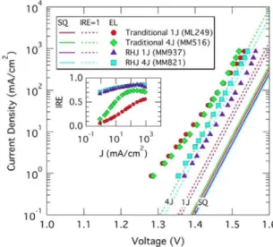
Fig. 6. GalnP junction dark JV (and IRE inset) from EL measurements (mark-ers) within single and 4J devices, comparing the traditional and RHJ designs. The SQ (solid) and internal (dashed) radiative limits are shown as lines.
While this study is focused on the GalnP top junction, it should be noted in passing that the GaAs junction performance (which is also a RHJ design in MM765) exceeds 97% IRE at high currents, though begins to drop due to n = 2 nonradia-tive recombination at slightly higher currents than the GalnP top junction. In addition, the GaAs junction of these inverted tandems clearly takes advantage of the gold BSR as evidenced by the fact that the internal radiative limit of the GaAs junction is much closer to the SQ limit than is the GalnP junction [see Fig. 5(a) and (b)]. Indeed, inverted 2 J GalnP/GaAs tandem cells of this design currently holds the world record efficiencies for 2J devices with 31.1% at one-sun AMI .5 global [16] and 34.1% at 467-suns AMI.5 direct.
IV. FOUR JUNCTION-INVERTED METAMORPHIC SOLAR CELLS
10
l i o3
<
I 2
•(fl
C i
S 1 0
10
= (a) 4th;/ 3rd/1 2, hst/
0 ¡/ £7 i / / /
• / / / / / / ' /
: o ;/ ••• / * / • /
r ¡H
o :/ • : /1
5 • /1/
-•f i
M
m
a
r 1
f/
7
I
- ¡1 Á Ü \l lit i
1
1
"1
. 11
:
0.5 1.0 1.5
Voltage (V)
10
= io-1
!
íio"z
fe-"--100% IRE 4tb Junction^ -"
10
- S i
(b)
^ « M ^ M
10
..i-Ai . . — • • • » * * " • • • • • • • * # * • • • " • *
uiül 1_ I
, a °°° '
10 10
Current Density (mA/cm )
1 „ Internal Radiative Limit
I . U i—i i mini .1 0.8
<u 0.6
18 0 . 4
-£ "in
£ 0.2
0.0
i nirrif—r r i n u n — T T T T
(e)
IT ¡111 A I T rrrin
• V * * * • *
• 1st 1.8 eVGalnP
* 2 n d l . 4 e V G a A s
• 3 r d 1 . 0 e V G a l n A s O 4th 0.7 eV GatnAs
lililí "A iltl I 10 10 10 10 10 10
Current Density (mA/cm )
Fig. 7. EL measurements (markers) represented in terms of (a) voltage, (b) ERE, and (c) IRE of inverted 4J IMM solar cell (MM821) with SQ (solid lines or pink highlights) and internal (dashed lines or yellow highlights) radiative limits. The light dotted lines are an attempt to fit each junction to the two-diode model as used in fig. 8.
to the GaAs substrate, while the third and fourth junctions are lattice-mismatched 1.0-eVIn 2sGa.7SAs and0.7-eVIn 5Ga.sAs junctions grown by metamorphic growth using two GaxIni_xP compositionally graded buffer layers [22]. The coupled EL and LC techniques described in the previous section can be used in the same way for 3 J and 4 J IMM solar cells [20], but we focus on the analysis of a 4 J here.
Fig. 6 shows a comparison of the dark JV curves of four dif-ferent GalnP junctions determined from EL measurements. The comparison shows both traditional and RHJ top junctions within 1J and 4J devices along with the SQ and internal radiative lim-its. Clearly both traditional junctions suffer from high J02 from nonradiative recombination at low currents, while the RHJs do not (down to ~ 1 mA/cm2). In addition, the JQ\ of the RHJ within the 4 J appears lower than J0i in the traditional junction within the 4 J which results in an advantage even at high concentrations. While the IRE of the two RHJs are nearly identical (see Fig. 6), the optical environment of the inverted U device including a gold BSR allows the internal radiative limit and actual results to more closely approach the SQ limit, compared with the RHJ in the 4J IMM where there is no reflector. However, the enhanced optical environment of the 1J also magnifies the effects of any recombination losses, so while the data for the top RHJ in the 4J IMM are quite close to the internal radiative limit, the data for the U RHJ are further away and the cell is not able to take full advantage of the gold BSR. The BSR of the U traditional junction does not boost the voltage compared to the
nonreflec-tive optical environment of the traditional junction within the 4J DVLM because the IRE is too low (except possibly at high currents).
Fig. 7 shows the equivalent 1) V(J), 2) r/ext(J), and 3) rfrnt(J)
characteristics from (LC corrected) EL of all four junctions within a 4 J IMM using the RHJ design in the top two junctions. The IRE of the top two junctions in Fig. 7(c) are quite similar to the IRE of MM765 in Fig. 5(c), though the ERE of the second junction is reduced due to the change in optical environment from a gold BSR to subsequent junctions. In this 4 J DVLM, only the fourth junction includes a gold BSR, which brings the inter-nal radiative limit closer to the SQ limit, but the relatively low
IRE of the fourth junction does not result in much advantage of the BSR. Actually, the IRE of this fourth junction is surpris-ingly high considering the mid- 106 cm2 threading dislocations (TDD) [22]. The IRE of the third junction is higher due to even lower TDD [23] (~106 cm2). In fact, at high concentrations (or current densities), the performance of the top three junctions in this 4J IMM are very close to the internal radiative limit. This means that the only way to dramatically improve the volt-age of this device at high concentrations is to either improve the fourth junction by reducing the TDD or changing the opti-cal environment of the top three junctions. We have considered techniques to incorporate omnidirectional selective reflectors by inserting distributed Bragg reflectors [24] or low index layers [25] between junctions to attain this improvement. However, the application of these interjunction reflectors has so far remained elusive. Instead, we note that the LC that naturally occurs with-out selective reflectors is also advantageous to the efficiency of 4J IMM solar cells. Characterization of the LC in this 4J IMM shows relatively strong coupling between each adjacent junction, which counter-intuitively, also increases the voltage of the entire device [19], [26]. In addition, the effects of LC are advantageous to reduce spectral sensitivity under real world conditions [27], [28].
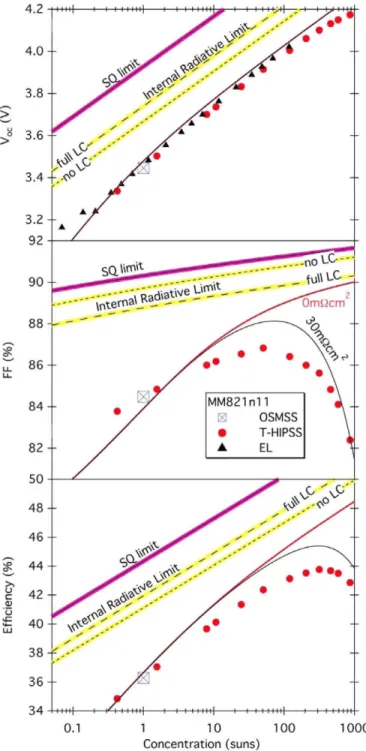
0.1 1 10 100 1000 Concentration (suns)
Fig. 8. 4JIMM solar cell performance (markers) as a function of concentra-tion. SQ (pink) and internal (yellow) radiative limits are shown. The internal radiative limit is shown including and excluding the effects of LC. The black (finite series resistance) and red (no series resistance) lines show predictions based on a two-diode fit to the coupled EL and LC measurements.
the predictions of the coupled LC and EL analysis of the actual device, fitting the performance of each junction to a two diode (n = 1 and n = 2) model (see dotted lines in Fig. 7) and again combining as described in [19], are presented as red and black lines in Fig. 8. While this prediction shows fairly good agree-ment with the flash data, it is not completely accurate because the nonradiative recombination cannot always be described by a simple n = 2 model. In particular, the third and fourth junctions
in Fig. 7(c) are not as well-fit using this two-diode model as the top two junctions are.
V. CONCLUSION
Inverted multijunction solar cells using a RHJ design for the top GalnP junction dramatically reduce the nonradiative recom-bination of that junction resulting in high IRE. This high IRE manifests as higher overall device voltages at all concentrations, but especially at low concentration, as well as increased LC that also improves efficiency and decreases spectral sensitivity in real-world applications. We have demonstrated the usefulness of reciprocity relations and optical modeling to directly com-pare the measured performance of individual junctions within multijunction devices. We also compare the measured perfor-mance with the well-known SQ (or external radiative limit) and with an internal radiative limit that we propose to account for the optical environment.
ACKNOWLEDGMENT
The authors would like to thank W. Olavarria, M. Young, S. Ward, and A. Duda for growth and fabrication of devices, T. Moriarty and C. Osterwald for official device results, and E. Yablonovitch for useful discussions.
REFERENCES
[1] W. Shockley and H. J. Queisser, "Detailed balance limit of efficiency of p-n junction solar cells," J. Appl. Phys., vol. 32, pp. 510-519, 1961. [2] U. Rau, "Reciprocity relation between photovoltaic quantum efficiency
and electroluminescent emission of solar cells," Phys. Rev. B, vol. 76, pp. 085303-1-085303-8, 2007.
[3] O. D. Miller, E. Yablonovitch, and S. R. Kurtz, "Strong internal and ex-ternal luminescence as solar cells approach the Shockley-Queisser limit,"
IEEE J. Photovoltaics, vol. 2, no. 3, pp. 303-311, Jun. 2012.
[4] M. A. Green, "Radiative efficiency of state-of-the-art photovoltaic cells,"
Prog. Photovoltaics, vol. 20, pp. 472-476, 2012.
[5] S. Roensch, R. Hoheisel, F. Dimroth, and A. W. Bett, "Subcell I-V char-acteristic analysis of GalnP/GalnAs/Ge solar cells using electrolumines-cence measurements," Appl. Phys. Lett, vol. 98, pp. 251113-1-251113-3, 2011.
[6] T. Kirchartz, U. Rau, M. Hermle, A. W. Bett, A. Helbig, and J. H. Werner, "Internal voltages in GalnP/GalnAs/Ge multijunction solar cells deter-mined by electroluminescence measurements," Appl. Phys. Lett, vol. 92, pp. 123502-1-123502-3, 2008.
[7] J. F. Geisz, M. A. Steiner, I. Garcia, S. R. Kurtz, and D. J. Friedman, "Enhanced external radiative efficiency for 20.8% efficient single-junction GalnP solar cells," Appl. Phys. Lett, vol. 103, pp. 041118-1-041118-5, 2013.
[8] M. A. Steiner and J. F. Geisz, "Non-linear luminescent coupling in series-connected multijunction solar cells," Appl. Phys. Lett, vol. 100, pp. 251106-1-251106-5, 2012.
[9] M. A. Steiner, J. F. Geisz, I. Garcia, D. J. Friedman, A. Duda, and S. R. Kurtz, "Optical enhancement of the open-circuit voltage in high quality GaAs solar cells," J. Appl. Phys., vol. 113, pp. 123109-1-123109-11,2013.
[10] T. Takamoto, E. Ikeda, H. Kurita, and M. Ohmori, "Structural optimiza-tion for single juncoptimiza-tion InGaP solar cells," Sol. Energy Mater. Sol. Cells, vol. 35, pp. 25-31, 1994.
[11] J. F. Geisz, "Application of III-V semiconductor heterostructures to optical chemical sensing," Ph.D. dissertation, Dept. Chem. Eng., Univ. Wisconsin-Madison, Wisconsin-Madison, WI, USA, 1995.
[13] F. W. Ragay, E. W. M. Ruigrok, and J. H. Wolter, "GaAs-AlGaAs het-erojunction solar cells with increased open-circuit voltage," in Proc. 1st
World Conf. Photovoltaic Energy Convers., 1994, pp. 1934-1937.
[14] J. F. Geisz, S. R. Kurtz, M. W. Wanlass, J. S. Ward, A. Duda, D. J. Friedman, J. M. Olson, W. E. McMahon, T. Moriarty, and J. Kiehl, "High-efficiency GalnP/GaAs/InGaAs triple-junction solar cells grown inverted with a metamorphic bottom junction," Appl. Phys. Lett, vol. 91. pp. 023502-1-023502-3, 2007.
[15] E. Centurioni, "Generalized matrix method for calculation of internal light energy flux in mixed coherent and incoherent multilayers," Appl. Opt, vol. 44, pp. 7532-7539, 2005.
[16] M. A. Steiner, J. F. Geisz, I. Garcia, D. J. Friedman, A. Duda, W. J. Olavarria, M. Young, D. Kuciauskas, and S. R. Kurtz, "Effects of internal luminescence and internal optics on Vo c and Jsc of III-V solar cells," IEEE J. Photovoltaics, vol. 3, no. 4, pp. 1437-1442, Oct. 2013.
[17] M. P. Lumb, M. A. Steiner, J. F. Geisz, and R. J. Walters, "Analytical modeling of III-V solar cells close to the fundamental limit," Proc. SPIE, vol. 8981, pp. 898114-1-898114-9, 2014.
[18] M. A. Steiner, J. F. Geisz, T. E. Moriarty, R. M. France, W. E. McMahon, J. M. Olson, S. R. Kurtz, and D. J. Friedman, "Measuring IV curves and subcell photocurrents in the presence of luminescent coupling," IEEE J.
Photovoltaics, vol. 3, no. 2, pp. 879-887, Apr. 2013.
[19] D. J. Friedman, J. F. Geisz, and M. A. Steiner, "Analysis of multijunc-tion solar cells current-voltage characteristics in the presence of lumi-nescent coupling," IEEE J. Photovoltaics, vol. 3, no. 4, pp. 1429-1436, Oct. 2013.
[20] J. F. Geisz, R. M. France, I. Garcia, M. A. Steiner, and D. J. Friedman, "Device characterization for design optimization of 4 junction inverted metamorphic concentrator solar cells," AIP Conf. Proc, vol. 1616, pp. 114-118,2014.
[21] R. M. France, J. F. Geisz, M. A. Steiner, I. García, W. E. McMahon, and D. J. Friedman, "Quadruple junction inverted metamorphic concentrator devices," IEEE J. Photovoltaics, 2014, to be published.
[22] R. M. France, I. Garcia, W. E. McMahon, A. G. Norman, J. Simon, J. F. Geisz, D. J. Friedman, and M. J. Romero, "Lattice-mismatched 0.7-eV GalnAs solar cells grown on GaAs using GalnP compositionally graded buffers," IEEE J. Photovoltaics, vol. 4, no. 1, pp. 190-195, Jan. 2014. [23] R. M. France, J. F. Geisz, M. A. Steiner, B. To, M. J. Romero, W. J.
Olavar-ria, and R. R. King, "Reduction of Crosshatch roughness and threading dislocation density in metamorphic GalnP buffers and GalnAs solar cells,"
J. Appl. Phys., vol. I l l , pp. 103528-1-103528-7, 2012.
[24] I. Garcia, J. Geisz, M. Steiner, J. Olson, D. Friedman, and S. Kurtz, "Design of semiconductor-based back reflectors for high Vo c monolithic multijunction solar cells," in Proc. 38th IEEE Photovoltaic Spec. Conf., 2012, pp. 002042-002047.
[25] I. Garcia, C. F. Kearns-McCoy, J. S. Ward, M. A. Steiner, J. F. Geisz, and S. R. Kurtz, "Back reflectors based on buried AI2 O3 for enhancement of photon recycling in monolithic, on-substrate III-V solar cells," Appl. Phys.
Lett, vol. 105, pp. 133507-1-133507-5, 2014.
[26] D. J. Friedman, J. F. Geisz, and M. A. Steiner, "Effect of luminescent coupling on the optimal design of multijunction solar cells," IEEE J.
Photovoltaics, vol. 4, no. 3, pp. 986-990, May 2014.
[27] A. S. Brown and M. A. Green, "Radiative coupling as a means to re-duce spectral mismatch in monolithic tandem solar cell stacks-theoretical considerations," in Proc. 29th IEEE Photovoltaic Spec. Conf, 2002, pp. 868-871.
[28] I. Garcia, W. E. McMahon, M. A. Steiner, J. F. Geisz, A. Habte, and D. J. Friedman, "Optimization of multijunction solar cells through indoor energy yield measurements," IEEE J. Photovoltaics, 2014, to be published. [29] C. R. Osterwald, M. W. Wanlass, T. Moriarty, M. A. Steiner, and
K. A. Emery, "Empirical procedure to correct concentrator cell efficiency measurement errors caused by unfiltered Xenon flash solar simulators," in
Proc. 40th IEEE Photovoltaic Spec. Conf, 2014.

![Fig. 5 shows three equivalent representations [using (l)-(3)] of the LC-corrected EL data that separately characterize the top and bottom junctions as 1) V(J), 2) iy e xt(J), and 3) í7¡ nt (J)](https://thumb-us.123doks.com/thumbv2/123dok_es/6857113.838303/3.891.502.787.95.348/shows-equivalent-representations-using-corrected-separately-characterize-junctions.webp)