Doctorado en Ciencias Naturales para el Desarrollo Escuela de Ingenier´ıa Electr´onica
A methodology for automated design and implementation of
complex analog and digital CMOS integrated circuits applying a
genetic algorithm and a CAD tool for multiobjective optimization
Tesis para optar por el grado de Doctor
Roberto Pereira Arroyo
Abstract
This dissertation proposes an automated methodology to design and optimize electronic inte-grated circuits, something that could be called simulation-driven optimization. The concept of Pareto optimality or the so called Pareto front is introduced as a useful analysis tool in order to explore the design space of such circuits. A genetic algorithm (GA) is employed to automatically detect this front in a process that efficiently finds optimal parameterizations and their corresponding values in an aggregate fitness space. Since the problem at hand is inherently a multi-objective optimization task, many different performance measures of the circuits must be able to be easily defined and computed as fitness functions.
The methodology has been validated through measurements of several fabricated test cases, using MOSIS fabrication services for a standard 0.5m CMOS technology.
Acknowlegments
Many people have helped me during these years of work and deserve my deepest gratitude. Dr. Alfonso Chac´on provided me with support, feedback and guidance. Dr. Pablo Al-varado, whom I shared seminal ideas and was always ready to give advice. Former students Leonardo Rivas, Frank Nicaragua, Dave Porras, Berny Dinarte, Jos´e Ibarra, Minor Coto and Roberto Molina spent many hours implementing test cases, trying different scenarios, which ultimately have provided part of the data presented in this dissertation. I also want to thank Dr. Renato Rimolo and Dr. Juan Luis Crespo for proofreading the draft document and giving valuable comments and suggestions.
Contents
List of Figures iii
Table index vii
1 Introduction 1
1.1 Goals and methodology . . . 3
1.2 Thesis outline . . . 4
2 Heuristic methods for multi-objective optimization 5 2.1 Current approaches for sizing and optimization of integrated circuits . . . 5
2.2 Genetic Algorithms . . . 8
2.2.1 Circuit Performance Evaluation using the Pareto Front . . . 9
2.3 Pareto Envelope-based Selection Algorithm . . . 10
2.3.1 CAD tool architecture and its implementation . . . 13
3 Application of automated methodology to CMOS circuit design 19 3.1 Optimization of MOS Current Mode Logic: a proof of concept . . . 20
3.2 A system for gunshot and chainsaw detection . . . 23
3.2.1 Optimization of an Operational Transconductance Amplifier . . . 27
3.2.2 Optimization of the Gm-C filters . . . 32
3.2.3 Optimization of the computing unit. . . 41
3.3 Optimization of a Self-biased Current Source . . . 44
4 Validation of the methodology through chip measurements 51 4.1 Measurement platform . . . 51
4.1.1 Employed hardware . . . 52
4.1.2 Printed circuit board (PCB) . . . 52
4.1.3 Software . . . 54
4.2 Measurements perfomed on fabricated circuits . . . 55
4.2.1 OTA experimental results . . . 55
4.2.2 SBCS experimental results . . . 55
4.2.3 GmC filter . . . 57
4.2.4 Computing unit . . . 59
5 Circuit optimization considering mismatch 61 5.1 Mismatch modeling . . . 61
5.2 Mismatch aware design process . . . 63
5.3 OTA optimization considering mismatch . . . 66
6 Conclusion 73
Bibliography 75
A Optimization tool user’s manual 81
A.1 Circuits’ Parameter Definition . . . 81
B ltilib-pareto 85
B.1 simInterface . . . 86
C Execution of the tool 89
D Processing of results 91
E Generation of the Pareto front graph 93
List of Figures
2.9 General optimization methodology implementation flow diagram . . . 15
2.10 Flow diagrams of fitness functions implementations I . . . 16
2.11 Flow diagrams of fitness functions implementations II . . . 17
3.1 MCML inverter/buffer. Transistors at the differential pair and at the ac-tive loads have identical dimensions. Therefore their naming as “MA” and “MLoad”, respectively. . . 21
3.2 An example of a 2-level MCML gate, implementing both Nand/And logic functions. . . 23
3.9 Architecture of filter bank and the detector, as based on the structure pro-posed in[10]. The filter is implemented Gm-C circuits, which entails the need for low power, highly linear OTAs. . . 27
3.10 Esquem´atico del OTA de 192nS. . . 28
3.11 Pareto front of the designed OTA. The graphic contains three metrics: input capacitance, transconductance and linear voltage range. . . 29
3.12 Output current curve as a function of the input voltage. The slope of this curve gives the circuit transconductance. All the waveforms presented are obtained with Mentor Graphics Eldo simulator and EzWave viewer. . . 30
3.13 Gm curve as a function of the input voltage for the selected result . . . 31
3.14 Gm-C implementation of the CWT. . . 32
3.15 Post-layout magnitude frequency response of the Gm-C filter bank. Vint is the response for the intermediate node, after the input amplifier. . . 32
3.16 Circuit schematic for a 64nS OTA. . . 34
3.17 iout vrs Vd for the 192nS OTA. . . 34
3.18 Transconductance curve of the 192nS OTA. . . 35
3.19 Output current transient response for the 192nS OTA. . . 35
3.20 Optimized filter bank diagram, where the OTA stages correspond to the op-timization discussed in section3.2.1. . . 37
3.21 Theoretical magnitude frequency response. . . 37
3.22 Theoretical phase frequency response. . . 38
3.23 Current mirror biasing circuitry. . . 38
3.24 Magnitude frequency response for coefficients 3, 4, 5 and intermediate node. 39 3.25 Filter transient response for an input of 600Hz of frequency. . . 39
3.26 Filter transient behavior for 100mV peak input at several frequencies. . . 40
3.27 Schematic diagram for a two-stage comparator. . . 42
3.28 Comparator’s post-layout simulation for a sine wave input of 0,15V at 10kHz. 44 3.29 Circuit schematic of the whole computing unit. . . 45
3.30 Circuit schematic of the current rectifier. . . 46
3.31 Rectifier unit output from hand-made version[9], for a sinusoidal input of 500 Hz, 150 mV peak. See the obvious asymmetrical response, product of both the systematic and random DC offset from the OTAs and the comparator. This asymmetry impacts the performance of the whole computing unit. . . 46
3.32 Rectifiers’ output. A small distortion is still present near the tripping point of the rectifier. This distorition is, nonetheless, much smaller to that is seen in the original circuit (see [9]). . . 47
3.33 Circuit schematic of SBCScurrent source used for optimization, as proposed by[6]. . . 47
3.34 Pareto Front for optimization with Stacking A. . . 48
3.35 Pareto Front for optimization with Stacking B. . . 48
3.36 Current variation versus voltage variation for two of the three current source prototypes. Variation is slightly better for the first power supply (4.32%/V against 6.19%/V,), though its area is almost twice the second. In the end, the smaller source was chosen. . . 50
4.1 Traditional instrumentation (left) and software-based instrumentation,picture taken from [32] . . . 52
4.2 PXI platform . . . 53
4.3 Shielding techique implemented in the PCB (red: tracks on top layer, green: tracks at bottom layer, yellow: layer overlap), also thin green and red tracks are guardlines connected to the SMUs. . . 53
4.4 PCB for testing, a two-layer board was used. . . 54
4.5 MeasuredGm curve as a function of the input voltage . . . 55
4.7 Dual SBCS output currents . . . 56
4.8 Reference currents in SBCS . . . 57
4.9 Filter time response . . . 58
4.10 Filter frequency response . . . 58
4.11 Filter coefficients offset . . . 59
4.12 Computing unit response . . . 59
5.1 Standard deviation ofVt versus the square root of the inverse area [46] . . . 62
5.2 Percent Standard deviationδβ/β versus the square root of the inverse area [45] 62 5.3 Circuit schematic for the OTA used for mismatch analysis. . . 64
5.4 Average power computation flow diagram . . . 64
5.5 Transconductance computation procedure . . . 64
5.6 Offset computation procedure . . . 65
5.7 Linear range computation procedure . . . 65
5.8 Bandwidth computation procedure . . . 65
5.9 Slew rate computation procedure . . . 66
5.10 Input capacitance computation procedure . . . 66
5.11 Standard deviation of the threshold voltage variation, (δVt) computation pro-cedure . . . 66
5.12 Current factor ((δβ/β)) computation procedure . . . 67
5.13 OTA’s output current as a function of input voltage . . . 68
5.14 Transconductance as a function of input voltage . . . 68
5.15 OTA’s frequency response . . . 69
5.16 OTA’s transient response. Top down:input voltage, output current and output voltage. . . 70
5.17 Current consumption(top) and offset current (bottom) for the transient response 70 A.1 Process for the parameterization of variables. . . 82
A.2 Example of parameter definition. . . 83
Table index
2.1 PESA Parameters and Typical Values . . . 13
3.1 Extraction of parametrizations for several MCML gates . . . 22
3.2 Performance measures of MCML gates, as obtained from post-layot simulations 22 3.3 Extraction of some representative results given by the optimization tool . . . 29
3.4 Simulation results for the best case OTA . . . 30
3.5 Transistor dimensions for the best case OTA . . . 31
3.6 Unitary transistor dimensions for the OTAs. . . 33
3.7 Performance features of the 192nS OTA. . . 35
3.8 Associated capacitance and Gm values in the filter bank. . . 36
3.9 Frequency response magnitude variations for each coefficient due to change in C10. . . 39
3.10 Filter’s obtained features vs initial ones. . . 40
3.11 Filter bank’s current consumption at 4V. IC implemented in [9]. . . 40
3.12 Output offset voltage for the filter bank. . . 41
3.13 Initial parameters for the comparator, with a bias current of 20µA . . . 42
3.14 Comparator’s fitness values. . . 43
3.15 Comparator’s postlayout characteristics. . . 43
3.16 Bias and current consumption for circuit implemented in[9]. . . 44
3.17 Final characteristics of the optimized comparator for the rectifier. . . 44
3.18 Best SBCS’s obtained after optimization, based on schemes Stacking A and Stacking B. . . 49
3.19 Transistor dimensions for two selected SBCSs. . . 49
3.20 Drain Currents (ID) and inversion indexes (if) for SBCS design of Stacking Ay Stacking B. . . 50
4.1 Output values for each SBCS. . . 57
4.2 Error percent for eachSBCS. . . 57
4.3 Output voltages and offsets for the GmC filter . . . 58
5.1 Parameters of the Amplifier. . . 67
5.2 Unitary transistor dimensions for the OTA, considering variability. . . 67
5.3 Performance features for the OTA, considering variability. . . 71
Chapter 1
Introduction
Analog integrated circuit design is a field that many consider as an art. In general, these kind of circuits contain an amount of parameters (variables) that the designer can adjust and, moreover, they have a direct impact on the perfomance of the circuit. Traditionally, analog design is made by hand using very general analytic equations in order to approximately describe the behavior of the circuit. Then, several (or many) simulations are performed to verify that the circuit works as expected. This is an iterative task and, usually, very time-consuming and furthermore, there is absolutely no guarantee about how optimum the resulting circuit is, for example, in terms of Silicon area, power consumption,slew rate, gain, offset, etc.
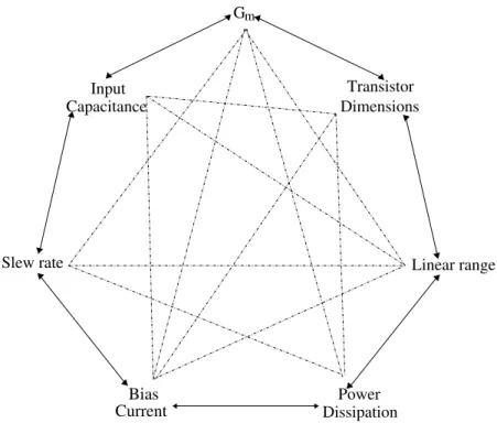
Another aspect that must be taken into consideration is the fact that usually it is needed to meet more that one design metric. This turns the task of exploring a given circuit’s design space into a multiobjective optimization problem. Thus, the basic problem is to find a trade off among design metrics: one cannot improve one without having a negative effect in the others. Fig. 1.1 shows a design heptagon which illustrates, with typical metrics, this trade off [48]
This dissertation introduces an automated optimization strategy that can be used for the fast and efficient design of CMOS electronic structures such as Operational Transconductance Amplifiers (OTAs), current supplies, MOS Current Mode Logic (MCML) gates and other analog and digital building blocks, taking advantage of the power and versatility of Genetic Algorithms (GAs). This not only significantly reduces circuit’s design time, but also ensures efficient and robust solutions. Some approaches [36], [29] tie the optimization problem to the specific topology of a circuit and to its parameters, making necessary a relative exhaustive search of the parameter space. Genetic Algorithms, on the other hand, work at a higher level of abstraction in which specific information about the circuit being optimized is not required: the GA only receives a set of fitness values (e. g. real numbers), representing circuit metrics such as power consumption, area, slew rate, etc. The proposed optimizer uses the genetic algorithm named PESA (Pareto Envelope-based Selection Algorithm) [11], and relies on a standard circuit simulator (e. g. EldoTM, SpectreTM, SPICE and alike) to deal with the
complexity of physical MOS transistor parameters and circuit topology. Circuit parameters
m
G
Input Capacitance
Transistor Dimensions
Current
Bias Power
Dissipation
Slew rate Linear range
Figure 1.1: An example of the trade-off between design metrics.
like supply voltages, bias currents, width and length of transistors, etc., are generated by the genetic algorithm and given to the simulator, where the computation of the fitness values takes place. Thus, the designer can change either the optimization algorithm or the simulation models without much effort. Analog Design Automation has been a research topic for over 20 years [28]. Since then, there has been a continuous effort in order to develop this area [14,26,23]. Following this trend, we contribute by taking specific application examples and showing the usefulness of GAs, multi-objective optimization and the Pareto front for automating analog and digital design.
1.1
Goals and methodology
The general objective of this dissertation is to develop an automated methodology for de-signing and implementing complex analog and digital CMOS circuits, using multi-objective optimization CAD tools.
The following are specific goals of this dissertation:
1. To validate a genetic optimization tool that can be integrated into a commercial sub-micron CMOS IC design flow.
2. To propose a circuit performance evaluation framework in order to feed the automated design space exploration and subsequent Pareto front generation.
3. To propose a framework for the generation and evaluation of the design space of sub-micron CMOS ICs, including the effect of process variability on the optimization. 4. To prove the efficiency of the methodolgy by implementing and verifying at least three
complex CMOS analog and digital cases.
In order to achieve the aforementioned specific goals, a number of tasks or problems are required to be solved, namely:
1. To establish a solid software interface between the algorithmic implementation and a commercial SPICE simulator. This interface has to be independent of the Genetic Algorithm and also should not be bound to any specific simulator.
2. The required circuit performance computation routines for integrating the tool into a commercial simulator must be implemented.This means that, starting from the stan-dard functions of a simulator, more complex functions must be derived in an automated way.
3. A Pareto front can have more than three dimensions. Thus a straightforward analysis routine must also be implemented in order to quickly process the results, when the front is four-dimensional or higher.
4. A variability model, previously justified and verified, must be integrated into the tool, such that not only more robust designs can be obtained but also ones whose precision can be predicted.
5. The effectiveness of the methodology will include three complex test cases, namely: • An low-power analog signal processing circuit for gunshot detection in forest
en-vironments.
• An low-power, temperature and voltage variation-tolerant current source. • A family of high-speed MCML cells.
The verification includes fabrication, circuit characterization through measurements and contrast with results from non-optimized prototypes or other examples reported in the literature.
1.2
Thesis outline
Chapter 2introduces heuristic optimization methods, such as Genetic Algorithms, how they work as well as the architecture of the electronic design automation (EDA)tool developed as part of this dissertation.
Chapter3 elaborates on examples of typical problems faced in classic, hand-made CMOS analog design, along with the significant improvement in the design process and the final results obtained after using the proposed Genetic CAD tool.
Chapter4shows the process followed in the development of a test platform for the fabricated application specific integrated circuits (ASIC) as well as the corresponding measurement results.
Chapter5defines the strategy to be applied for the analysis of variability in selected designed structures, based on the model proposed by Pelgrom [46].
Chapter 2
Heuristic methods for multi-objective
optimization
Heuristic optimization methods, such as Genetic Algorithms, are essentially computational and therefore have been increasingly applied following the development of electronic comput-ing devices [25]. The heuristic optimization paradigm is based on concepts found in nature; for example, the principle of evolution through selection and mutation (genetic algorithms), the annealing process of melted metals (simulated annealing) or the self-organization of ant colonies (ant colony optimization). What is expected in general from a heuristic? First, a heuristic should be able to provide high quality (stochastic) approximations to the global optimum, but it is not supposed to give the exact solution to the problem. Second, a well behaved heuristic should be robust to changes in problem characteristics, i. e. it should not only fit a single problem instance, but a whole class of problems. Third, a heuristic should be easily implemented regardless of any arbitrary number of problem instances and, even if the heuristic is stochastic, it should not contain subjective elements. Given the above defi-nition of heuristics, one of their major advantages consists in the fact that their application does not rely on a set of strong assumptions about the optimization problem; it suffices the possibility to evaluate the objective function for a given element of the search space. No assumption on some global property of the objective function is required, nor the computa-tion of its derivatives (common in classic optimizacomputa-tion strategies). Therefore, the problem of optimizing analog and digital integrated circuits meets many if not all of the requirements that make a problem a good candidate for a heuristic solution.
2.1
Current approaches for sizing and optimization of
integrated circuits
As briefly stated before, various methods have been published for calculating the performance features of CMOS digital and analog integrated circuits. These methods offer a broad range of possibilities depending on the way the circuit performances are obtained, wether or not
transistor mismatch is considered and, mainly, what kind of algoritm is used to solve the optimization problem (deterministic or heuristic, global or local optimizer).
A deterministic optimization approach, shown in [30] is called Geometric Programming (GP). A geometric program is an optimization problem of the form:
minimize f0(x),
the optimization process is very fast, the GP can only optimize over a convex function and the performances and constraints must be expressed as posynomial functions. This is a task that can be time-consuming and it is bound to a specific circuit topology. In the end, the accuracy of this simplified circuit’s model must be verified against Spice simulations. While geometric programming is certainly known, it is nowhere near as widely known as, say, linear programming. In addition, advances in general-purpose nonlinear constrained optimization algorithms and codes have contributed to decreased use (and knowledge) of geometric programming [30].
Another approach, Linear programming (LP) is an optimization method that has been used since World War II. In LP the objective function is linear and all constraints can be supplied as linear equalities or inequalities. More formally, a LP can be expressed as:
maximize CTx,
subject to: Ax<b (2.2)
Here, x represents the decision variables of the LP, which are the design parameters. The CTxobjective function is some linear function ofxthat is determined by what we are trying to optimize (e.g.: gain,bandwidth, slew rate, etc.). The equations Ax<b represent the set of constraints which essentially relate some linear transformation of x to a constant b. It should be noted that any inequality or equality constraint can be put into this form. There are several algorithms that are able to solve LPs and its variants in an efficient manner, the Simplex or Dantzig algorithm being one of the most popular [13].
In similar way as in Geometric Programming, the Linear Programming method requires an understanding of circuit topologies and equations for the objective functions of interest, i.e. a linear model of each specific circuit must be derived. For example in [8] the algorithm requires an objective function, upper and lower bounds for all voltage nodes, and a set of inequalities that force all transistors to operate in saturation.
Simulated Annealing is a stochastic method that has been used for analog circuit optimiza-tion for over 20 years [24, 37].
cool-ing it very slowly to the ambient temperature until perfect crystals emerge. The quality of the results strongly depends on the cooling temperature. The final state can be interpreted as an energy state (crystaline potential energy) which is lowest if a perfectly crystal emerged. If we compare optimization to the annealing process, the attainment of a global optimum is analogous to the attainment of a good crystal structure. Simulated annealing was intro-duced in [34]. Fig. 2.1 shows the correspondig pseudocode. The core of the algorithm is the Metropolis procedure, which simulate the annealing process at a given temperature T [38].Metropolis also receives the current solution S which it improves thorough local search. It must also be provided with the value M, which is the amount of time that annealing must be applied, at a given temperature. The procedure Simulated annealing simply in-vokesMetropolis at various (decreasing) temperatures. Temperature is initialized to a value
T0 at the beginning of the procedure, and is slowly reduced in a geometric progression; the
parameterαis used to achieve this cooling behavior. The amount of time spent in annealing at a temperature is gradually increased as temperature is decreased. This is done using the parameterβ >1. The variable Time keeps track of the time being expended in each call to the Metropolis. The annealing procedure halts when Time exceeds the allowed time.
Algorithm: Simulated Annealing
Figure 2.1: Pseudo code for a Simulated Annealing algorithm.
greedy-fashion towards the minimum.
Algorithm: Metropolis(S,T,M)
1: repeat
2: NewS=neighbor(S)
3: ∆h=Cost(New(S)-Cost(S)
4: if ∆h <0 or random < e−∆h/T then
5: S=NewS
6: end if
7: M =M −1
8: until M = 0
Figure 2.2: Pseudocode for the Metropolis procedure
Although, as already stated, simulating annealing has been around for many years, these approaches generally treat the multiobjective problem by deriving a circuit-specific equation which hopefully will reflect the effect of single objectives. In other words, the concept of Pareto optimality is not used. Related approaches like the one reported in [22] relies on the fact that optimization carried out over a metamodel (which is an abstracted representation of the circuit model) instead of the actual circuit will allow fast design space exploration and reduce the design cycle time. In that paper three different optimization algorithms are compared: exhaustive search, tabu search and simulated annealing algorithms are analyzed to determine their suitability for metamodeling-based optimization, however their results are not necessarily applicable for transistor-level simulation as it is the approach presented in this dissertation.
2.2
Genetic Algorithms
Genetic algorithms imitate the evolutionary process of species that sexually reproduce. New candidates for the solution are generated with a mechanism called crossover which combines part of the genetic material of each parent and then applies a random mutation. If the new individual, called child, inherits good characteristics from its parents it will have a higher probability to survive. The fitness of the child and parent population is evaluated in function survive(statement 10 in pseudo code shown below) and the survivors can be formed either by the last generated individualsP00,P00 ∪ {the fittest from P0}, only the fittest from P00 or
the fittest from P0∪ P00. A pseudo code for genetic algorithms is shown in Fig. 2.3.
Algorithm: Genetic algorithms.
1: Generate initial population P of solutions
2: while stop criterion not metdo
3: Select P0 ⊂ P (mating pool), initialize P00 (set of children)
4: for i= 1 . . .n do
5: Select individuals xa and xb at random from P0 6: Apply crossover to xa and xb to produce xchild 7: Randomly mutate produced childxchild
8: P00← P00∪x
child 9: end for
10: P ←survive (P0,P00)
11: end while
Figure 2.3: Pseudo code for a genetic algorithm.
2.2.1
Circuit Performance Evaluation using the Pareto Front
The aggregate fitness function F for a circuit A with the parameterization u is defined as:
F(Au) = Φ(f1(Au), f2(Au), . . . , fn(Au)) (2.3)
With the individual fitness functions fi(Au) defined to increase monotonically with the
fitness of some particular aspect of the circuit’s behavior. For example, if the objective is to optimize an OTA (Operational Transconductance Amplifier), fitness values like linear range and the slew rate may be directly related. On the other hand, the input capacitance and the transconductance are inversely related to preserve the condition of increasing monotonicity. The functions fi span a multidimensional fitness space, where each point represents the
performance of a circuit parameterized with one point u in a parameter space. The general form of Φ is assumed unknown, but it has to increase monotonically with increasing values of all fitness functions fi. This condition ensures that a point in the fitness space can be
considered fitter than all other points with smaller values in all dimensions. In Fig. 2.4, for example, the point q1 is fitter than the point q4 and all other elements within the gray
rectangle. In this context, the point q1 is said to dominate q4. All non-dominated points
in a set define the Pareto front of that set. In the example of Fig. 2.4 this front is defined by the points q1, q2, q3. Choosing a parameterization that is not in the front is always a
bad choice, since there is another point on the front with a better aggregate fitness. The previous concepts can be expressed mathematically using the following equation:
ˆ
P ={hu ∈ PA,f(Au)i|¬∃v ∈ PA:f(Av) f(Au)} (2.4)
where ˆP is the Pareto front, f is the vector of fitness functions [f1, ..., fn] T
and PA is the
f1
f2
q1
q2
q3
q4
Figure 2.4: Pareto front in a two-dimensional fitness space.
f(Av)f(Au)⇔
∀i:fi(Av)≥fi(Au)∧ ∃i:fi(Av)> fi(Au)
(2.5)
The evaluation process can therefore be considered as a mapping process that transforms the valid parameter spacePA into a connected region in the fitness space [f1, . . . , fn]T. The
Pareto Front is the border of this region delimited by the partial optima [40]. Any algorithm that finds the Pareto front for a set of fitness points implements eqs. (2.4) and (2.5). Since the parameter space PA usually contains an infinite number of parameterizations, the next
problem consists in choosing a representative set of samples fromPA, such that their Pareto
front can be assumed to be a reliable approximation of the exact front extracted for the complete space. A naive approach would be to regularly sample the values of each parameter, since the number of necessary evaluations will increase exponentially with the number of parameters. For example, a circuit with seven parameters (design variables), each sampled five times, would require 57 = 78125 evaluations. To avoid this brute-force parameter search, here the multi-objective evolutionary algorithm PESA is employed. This genetic approach suppresses the computation of useless parameterizations and concentrate the analysis on those regions of the parameter space that provide promising results. Even if this algorithm also discretizes the parameter space, through a numeric representation with a finite number of bits, the resolution used for each parameter can be as high as necessary, without the menace of an exponential explosion of the search space. The number of evaluations required is then proportional to the number of bits used to represent a parameterization.
2.3
Pareto Envelope-based Selection Algorithm
Algorithm) by Corne et al. has been chosen in this work to seek for the Pareto front, since it has proven to perform better than other available techniques [11].
PESA is an evolutionary algorithm. The search for the non-dominated front relies on the principles of mutation and crossover of the currently fittest individuals. Mutation tries to improve a parameterization through a few random changes. It searches for fitter candidates in the neighborhood of previously found solutions. Crossover takes two parent candidates and combines them in order to generate a third, possibly fitter individual, where the combination makes it possible to sample a larger region of the parameter space.
In the PESA implementation, a parameterization (also phenotype) needs a binary represen-tation (chromosome). The mutation process inverts the value of a chromosome’s bit if a random number drawn from a uniform distribution between 0 and 1, is smaller than the desired mutation rate Pm. A uniform crossover technique is also used, in which each bit of
the child is inherited with the same probability from each parent.
The algorithm administrates two sets of phenotypes, calledpopulations. Theexternal popu-lationPE represents the current approximation of the Pareto front. Theinternal population
PI, usually smaller, contains a set of new candidates to be eventually included in the front.
To avoid the external front exceeding a predefined maximal size, some old elements may have to be removed. The selection of these individuals is the main difference between most Pareto evolutionary algorithms. PESA keeps track of the degree of crowding at different regions of the fitness space. It selects for removal those elements in the most dense sections, such that the phenotypes in the front tend to be equally distributed. The algorithm is outlined in Fig. 2.5.
The incorporation of non-dominated candidates into the Pareto front at line 4 includes the removal of all individuals that are dominated by the new incomers. This is necessary to maintain the consistency of PE. For the required crowding measure, Corne et al. have
originally suggested to partition the fitness space in regular hyper-boxes. A “squeeze factor” is then assigned to each box, defined as the total number of phenotypes within the box. This histogram-based density estimation is employed at line 6: an individual in the box with the highest squeeze factor is selected for removal. The opposite occurs in the choice of individuals for crossover and mutation (lines 11 and 13): a binary tournament strategy is used to direct the attention towards the least dense regions of the front, i. e. from a randomly chosen pair of individuals, the one with the smallest squeeze factor is always taken as parent, breaking ties randomly. Both actions help keeping the parameterizations equally distributed in the fitness subspace spanned by the Pareto front.
The crossover probability Pc at line 10 defines the fraction of new individuals that are
generated through crossover. The probability 1− Pc specifies, therefore, the number of
parameterizations obtained from mutation of a single parent.
Algorithm: PESA [11]
1: initialize the external populationPE with the empty set
2: initialize the internal populationPI with nI random individuals 3: repeat
4: find all individuals in PI that are not dominated by any
ele-ment of PI∪ PE and incorporate them into PE 5: while |PE|> nE do
6: select and remove an individual of PE 7: end while
8: remove all remaining elements of PI 9: while |PI|< nI do
10: if probability Pc then
11: select two parents from PE and produce single child by
crossover and mutation
12: else
13: select single parent from PE and produce single child by mutation 14: end if
15: add child to PI 16: end while
17: until maximum number of iterations is reached
18: return PE
Figure 2.5: Pareto Envelope-based Selection Algorithm
Here, an additional extension originally proposed in [1] has been “borrowed” from the sim-ulated annealing optimization techniques. The mutation rate is allowed to decrease asymp-totically from an initial value Pminitial towards the desired final rate Pmf inal, resembling the
temperature reduction typically found in such algorithms:
Pm = (Pminitial −Pmf inal) exp(i/τ) +Pmf inal (2.6)
with i the iteration number and τ the mutation decrease factor. The implementation has been integrated in an open source software library described in [16]. The increased mutation rates at the beginning stimulate a stronger random sampling of the parameter space. At early iteration stages the points in the front have not suffered a long evolution, and thus their parameter values are still relatively unstable. The random sampling accelerates the localization of fitter candidates. As soon as several iterations have confirmed the fitness of the points in the front, the random sampling becomes rather harmful to the process. Lower mutation rates give more weight to the information contained in the parents, which are at later iterations probably fitter than random candidates.
Table 2.1: PESA Parameters and Typical Values
Symbol Parameter Value
nI Size of the internal population|PI| 10
nE Size of the external population|PE| 100-200
Pc Crossover probability 0.7
Pminitial Mutation rate 3/chromosome size
Pmf inal Mutation rate 1/chromosome size
τ Mutation decrease factor 40
Maximum number of iterations 500-1500
Kernel size as fraction of the bounding-box size 1/32
Figs. 2.6 and 2.7 show the chromosome representation for a NAND gate and the OTA respectively. Bit strings were chosen to represent these chromosomes, defining minimum and maximum values for every parameter within the bit string. For example, in Fig. 2.7, the parameterIb (Bias current) uses 5 bits which enables 32 possible distinct values for this
parameter.
Figure 2.6: NAND gate chromosome
Figure 2.7: OTA chromosome
2.3.1
CAD tool architecture and its implementation
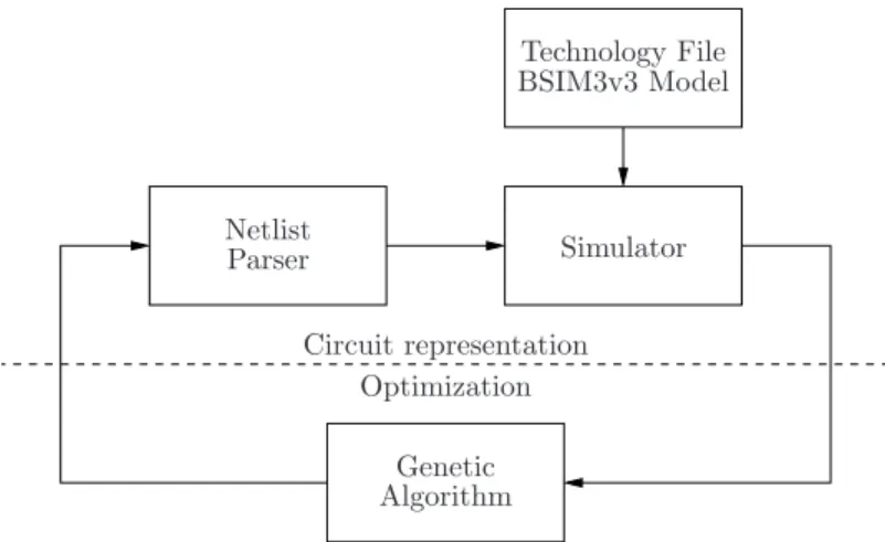
of BSIM1 with models provided from the semiconductor foundry). On the other hand,
the core of the optimization process is based on the LTI-Lib [16], an open source library originally intended for image processing research [16], which provides the implementation of the PESA algorithm and the generation of the Pareto front. In Fig. 2.8, the thick dotted line illustrates this separation of tasks. Furthermore, the optimization and representation processes are communicated through TCP/IP sockets, which allows for each process to reside on different machines or operating systems.
Genetic Algorithm Netlist
Parser Simulator
Technology File BSIM3v3 Model
Circuit representation Optimization
Figure 2.8: Optimization CAD tool block diagram.
Fig.2.9 presents a more detailed illustration of the steps followed in order to implement the optimization methodology.
Figs. 2.10 and 2.11 present flow diagrams for some of the routines that were implemented in order to compute different fitness functions. All of these routines process the output file generated after each simulation and basically search for a specific feature, for instance a node capacitance, or use the given data to calculate values like linear range or the transconduc-tance.
Chapter 3
Application of automated
methodology to CMOS circuit design
An optimized design of particular electronic cells usually kicks-off with a first-hand design stage based on a very approximate first order model, something that requires multiple itera-tions through a tiring process of hand re-calculation, simulation and fitting, in order to reach a limited set of specifications. The use of a heuristic tool, not only cuts down the process, since the designer is not forced to re-calculate using the first order model again, but it also allows for an increase in the set of specifications that usually require mutually exclusive goals that first order models are typically ill suited to reconcile. This case is particularly well illustrated in the case of submicrometric CMOS design, where the transistor models can easily become cumbersome, especially when trying the cover all the MOSFET regions of op-eration, from weak to strong inversion, either in saturation or in linear mode. Thus, for long channel MOSFET design, the use of a first order model such as the EKV [18] or ACM [21] models is limited to the the initial specification of the cell under design, a specification that is not necessarily enforced in this first stage, as the tool will be used to solve this task. And of course, in the case of short-channel design –where accurate first-hand models are largely unwieldy–, the designer can very well kick-start the process with an ill-fitted approximation, knowing that at worst, the optimization process will only require some extra iteration time. In this chapter, examples of typical problems faced in classic, hand-made CMOS analog and digital design are shown, along with the significant improvement in the design process and the final results obtained after using the proposed Genetic CAD tool, results that in many cases not only comply, but surpass the critical specifications given to the problem. In most of the cases, results are compared with published data of similar hand-made designs.
3.1
Optimization of MOS Current Mode Logic: a proof
of concept
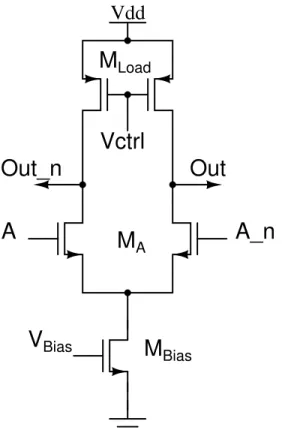
MCML is a circuit technique that has been used in applications of high-speed, mixed signal environments due to its reduced switching noise, immunity to common-mode noise and, espe-cially, because its power consumption does not increase with the frequency of operation[39], whereas in standard CMOS circuits, power consumption increases linearly with frequency. In[42] it is shown that MCML dissipates less power at operation frequencies of more than 300 MHz. More recently, it has also been shown that subthreshold MCML can be used to implement digital circuits at frequencies below a few megaherz, with a better power-delay product than CMOS counterparts[7]. However, designers have been reluctant to use MCML instead of CMOS due to the complexity of MCML and the lack of automation tools. This situation has made impossible to produce robust and power efficient designs at low cost and reasonable time to market[41]. The fundamental MCML inverter/buffer is shown in Fig.3.1. MCML circuits have three main components: PMOS transistor loads, one or more differen-tial pairs depending on the number of logic inputs and a constant current source, controlled by the voltageVbias. All logic inputs and outputs are fully differential. The circuit operation
is based on current steering, i. e. the tail current produced by the transistor Mbias is steered
into one of the branches depending on the differential inputs. This current develops a resis-tive voltage drop at the acresis-tive load of the conducting branch, while in the non conducting branch the output voltage is pulled to Vdd, thus producing complementary outputs. For a
single logic gate, its delay and power are respectively given by [42]:
DM CM L =C(∆V /I), (3.1)
PM CM L =I·Vdd, (3.2)
where C is the load capacitance, I is the tail current and ∆V is the output voltage swing. Equation (3.1) indicates that the propagation delay can be reduced by lowering the voltage swing, decreasing the load capacitance or increasing the tail current. However, from Eq. (3.2) it is seen that increasing the tail current directly impacts the power consumption.
If the circuit shown in Fig. 3.1 is operating in the mid swing point of its voltage transfer curve, the currents in the two branches are equal to I/2, both transistors in the differential pair are in saturation and their currents can be expressed as[5]:
I
where Ud is the mobility degradation coefficient, Ec the critical electric field for velocity
saturation, µ0 the permeability of vacuum, Cox the oxide capacitance per unit gate area, Vt
the threshold voltage and (W/L)A, VGSA are the width, length and gate-source voltage for
transistors MA, respectively.
Vdd
M
BiasM
LoadM
AVctrl
A
A_n
Out
Out_n
V
BiasFigure 3.1: MCML inverter/buffer. Transistors at the differential pair and at the active loads have identical dimensions. Therefore their naming as “MA” and “MLoad”, respectively.
circuit parameters can be varied by the designer, namely: (W, L) for Mbias, Ma and Mload
plus Vdd, Vctrl and Vbias.
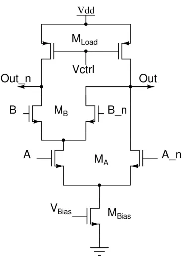
Fig.3.2shows an example of a 2-level MCML circuit. It has been shown in[29] how optimizing 2-level gates becomes even more complex, as more parameters come into play, making its design by hand calculations a task of little practical use. Therefore it is apparent the need for an optimization strategy that is automated and independent of circuit topology.
Fig. 3.3 shows the Pareto front of a MCML Xor. Three design metrics were defined for this example: voltage swing, average power consumption and propagation delay, although as previously stated, other metrics can also be defined.
Table 3.1 shows a list of some selected results from the Pareto front. Each column in the table contains the set of parameters defined for the corresponding logic gate.
It is necessary to point out that the optimization methodology is simulation-driven at the schematic level. The layout is not included within the optimization, mainly because there are not tools for fast automatic layout generation of analog cells, at least they were not available at the time of this research. The fact is that analog design still remains a mainly hand-made task. However, post-layout simulation results are presented as thay are supposed to be close to a fabricated circuit.
Table 3.1: Extraction of parametrizations for several MCML gates
Parameter Xor CarryOut Nand DFlip-Flop
Vdd (V) 2.7 2.7 2.7 2.7
Vbias (V) 2.7 2.7 2.7 2.7
Vcntrl (V) 0 0 0 0
Wbias(µm) 2.9 4.8 4.1 5.83
Lbias(µm) 0.65 1.5 1.22 0.43
Wa(µm) 4.8 2.58 3.45 3.95
La(µm) 2.48 0.75 1.22 0.43
Wb(µm) 2.9 5.15 3.1 5.65
Lb(µm) 0.75 0.65 0.9 1.53
Wc(µm) 5.14 4.2 -
-Lc(µm) 1.30 0.51 -
-WLoad(µm) 6 4.8 5.83 5.83
Load(µm) 2.72 0.83 0.75 0.83
Table 3.2: Performance measures of MCML gates, as obtained from post-layot simulations
Gate Power (mW) OutSwing (V) Delay (ns)
Xor 0.4 1.45 1.3
CarryOut 0.7 0.5 0.96
Nand 0.78 0.7 1.7
Vdd
M
BiasM
LoadM
AVctrl
A
A_n
Out
Out_n
V
BiasB
M
BB_n
Figure 3.2: An example of a 2-level MCML gate, implementing both Nand/And logic functions.
Fig. 3.5 shows the timing simulation.
Fig. 3.6 shows the simulation in order to determine gate delay. Fig. 3.7 shows the average power.
Fig. 3.8 shows the voltage swing.
3.2
A system for gunshot and chainsaw detection
The development of components of a wireless sensor network (WSN) for protection of tropical forests has been proposed in[2]. The ultimate goal is to detect gunshots (illegal hunting) and chainsaw noises (illegal timbering). The network’s sensor nodes must be deployed in remote locations, be almost maintenance free and powered from small batteries. Therefore, low power consumption is critical as the battery charge must last for long periods of time. A very low power ASIC1 implementation has been chosen, as its power consumption can feasibly be brought under a few dozens of micro-watts on a not so modern CMOS process (such as a 0.5µm commercial process), in contrast with any commercial
0
Figure 3.3: Xor Pareto front
based implementation or even a FPGA2 one, that easily surpass such limits.
Three phases characterize each node’s operation: impulsive sound detection, sound classifi-cation and a stage of spacial loclassifi-cation of sounds.
For the detection stage, a series of hardware algorithms were evaluated in order to determine the optima in terms on low power consumption and detection efficiency [10], and a hand-made first version of the resulting integrated circuit has been designed and tested, as shown in [9]. The circuit implements a continuous-time wavelet transform (CWT), as a simple way of performing signal detection and classification. Fig. 3.9 presents the detection stage, which is composed by a Gm-C filter bank that separates the input signal into three CWT coefficients whose maximum frequency is 875 Hz. Then an energy estimation is performed for each coefficient, their sum is computed and compared to an adaptive threshold, typically a running average or a RM S estimation of the same pre-processed signal, scaled by a gain factor.
The first problem at hand is to optimize the OTAs (Operational Transconductance Ampli-fiers) such that its power and parasitics are minimized, whereas slew rate, frequency response and linearity are maximized. This entails an more efficient filter, closer to the theoretical specifications given in [10], and that fixes the problems of its first version, as given in [9]: pole-shifting, excessive DC-offset and higher than expected power consumption due to the required adjustment of the filter’s poles (5.64µA from the expected 2.26µA of total bias cur-rent in the filter bank alone, due to the needed doubling of the OTAs’ bias (from 45 nA to
0 5000 10000 15000 20000 25000 30000 1.9 2
2.1 2.2 2.3 2.4
2.5 2.6 2.7 2.8 7
7.5 8
8.5 9
9.5 10
10.5 11
Log(1/Delay)
1/Power
Vout Swing Log(1/Delay)
Figure 3.4: A Pareto front for a MCML Nand gate
Figure 3.6: Delay measuremt in the simulation diagram
Figure 3.7: Average Power curve
(a) Architecture of the detector. (b) Filter bank equivalent.
Figure 3.9: Architecture of filter bank and the detector, as based on the structure proposed in[10]. The filter is implemented Gm-C circuits, which entails the need for low power, highly linear OTAs.
95.6 nA) in order to place the poles in the right frequencies). Though some of the problems in the first version are due to the final circuit’s layout parasitics and uncertainties unac-countable during the simulation process, it is clear that the minimization of the systematic defects in the design, should greatly compensate for post-fabrication random effects (this of course also opens an interesting problem for the CAD future development: how to integrate CMOS fabrication uncertainty models into it in order to account for such deviations during the optimization cycle, and minimize if possible their impact in the final design). As it was already mentioned, we envision that the Pelgrom model can be used as a way to determine transistor size constraints and feed them into the tool such that more robust circuits can be obtained.
3.2.1
Optimization of an Operational Transconductance Amplifier
As shown in[48], an operational transconductance amplifier is optimized in order to solve the problems of the CWT filter’s first implementation. See Fig. 3.10.
The output transconductance Gm can be approximated by:
Gm =
gm1
m(1 + gm1
4gm2)
, (3.4)
where m represents the scale factor due to the lower current mirror, gm1 and gm2 represent
the transconductance of transistors M1 and M2, respectively.
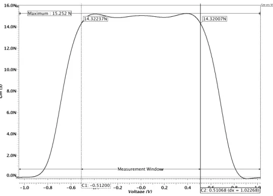
OTAs are specially characterized by their linear range of transconductance, defined as the differential input voltage range that produces a constant value of transconductance at the output. Since OTAs are not perfectly linear circuits, their transconductance can vary de-pending on the amplifier’s design and operating mode. Consequently, the designer must define the precision of its linear range, based on the variability than can be tolerated, distor-tion or the maximum deviadistor-tion in the circuit’s response. Most experiments and simuladistor-tions executed show that the linear range ∆V is directly proportional to the bias current in DC and to the dimensions of transistors M1 and M2:
Vdd
Figure 3.10: Esquem´atico delOTA de 192nS.
SR = 2·Ib
m·C (3.6)
SR= 2·Ib·(2πfc)
m·Gm
, (3.7)
Equations (3.4), (3.5), (3.6) and (3.7) show competing objectives, i. e. conflicting fitness functions. This means that it is not possible to find an single optimum for a design metric (either ∆V, SR orGm) without negatively affecting the other design metrics or fitness values.
The concepts related to optimization, genetic algorithms and the Pareto Front were detailed in Chapter 2. Building upon those concepts, Fig. 3.11 shows the three-dimensional Pareto front of the previously shown OTA. This front contains 1500 individuals (parametrizations) and it was generated by the PESA genetic algorithm. The graphic shows the design trade offs between the three parameters: in order to maximize one of these, the other parameters must decrease their values.
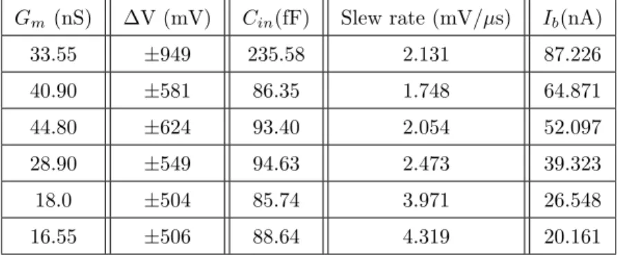
Table3.3contains a list of some selected results given by the optimization tool. These results contain cases with wide linear range, high transconductances, and/or low capacitances. The slew rate condition is fulfilled in low Gm values.
Figure 3.11: Pareto front of the designed OTA. The graphic contains three metrics: input capac-itance, transconductance and linear voltage range.
Table 3.3: Extraction of some representative results given by the optimization tool
Gm(nS) ∆V (mV) Cin(fF) Slew rate (mV/µs) Ib(nA)
33.55 ±949 235.58 2.131 87.226
40.90 ±581 86.35 1.748 64.871
44.80 ±624 93.40 2.054 52.097
28.90 ±549 94.63 2.473 39.323
18.0 ±504 85.74 3.971 26.548
of the circuit, which is obtained by calculating the slope of Fig. 3.12.
Figure 3.12: Output current curve as a function of the input voltage. The slope of this curve gives the circuit transconductance. All the waveforms presented are obtained with Mentor Graphics Eldo simulator and EzWave viewer.
Table 3.4 shows a summary of the simulations obtained for the best case OTA and the initial OTA, that shows the improvements obtained in comparison with the original design. The decrease of the transconductance value is a positive result because in order to keep the pole of the filter in the same place, when the transconductance is reduced it is necessary to reduce the capacitance too, producing a reduction of the circuit area. All of the other design specifications where also greatly improved: the input capacitance and power consumption were lowered while the linear range and the slew rate were greatly improved. Finally, Table
3.5 contains the unitary transistor dimensions given by the optimization tool. Table 3.4: Simulation results for the best case OTA
Measurement Best case OTA Initial OTA
MaximumGm (nS) 15.077 36.57
Linear range ∆V (mV) ±512 ±260
Slew rate (mV/µs) 3.676 1.954
Power consumption (nW) 144.3 174.93
Figure 3.13: Gm curve as a function of the input voltage for the selected result
Table 3.5: Transistor dimensions for the best case OTA
Parameter Value
L1(µm) 7.2
L2(µm) 8
L3(µm) 0.5
L5(µm) 5.4
W1(µm) 0.8
W2(µm) 0.8
W3(µm) 7.2
3.2.2
Optimization of the Gm-C filters
As discussed in [48], an operational transconductance amplifier has been optimized in order to minimize some of the the problems of the CWT filter’s first implementation. The use of a automatized tool for multiple objective design based on Genetic Algorithms made easier to obtain low transconductance, low power OTAs with a linear range over 1V. The complete filter is shown in Fig.3.14. A third order pass-band filter is used to obtain each coefficient. Some extra amplification is given at the input, and a high-pass filter gets rid of any DC offset from previous stages. This filter introduces an extra pole that is not considered in the theroretical relations specified in [10]. Its effect is minimized by placing it at a very low frequency, and it only impacts the cD5 coefficient (see Fig. 3.15 for the simulated frequency response of the whole CWT filter). This effect should not nonetheless present major deviations for the expected detection efficiency, as explained in [10]. was discussed in [10], this coefficient is only determinant in the minimization of false positives.
_
Figure 3.14: Gm-C implementation of the CWT.
100
Filter construction.
A full description of the process carried out in order to get rid of the problems of the first implementation, as reported in [9] is given. This implementation presented excesive power consumption, large parsitic capacitances and frequency pole-shifting in the filter bank. In the optimized implementation the structure of the filter was not touched but all components were resized in order to reduce the aforementioned problems.
A natural question would be why not to optimize the whole filter structure instead of di-viding it into blocks and individually optimizing each one? There is no single answer to this question but hierarchical design is well-established, simulation time grows with circuit complexity and, since the optimization strategy relies on thousands of simulations in order to achieve the evolutionary process, see section2.2.1, the total computing time would explode to prohibitive levels. Other optimization techniques were discussed in section2.1, although those techniques also work at the block level.
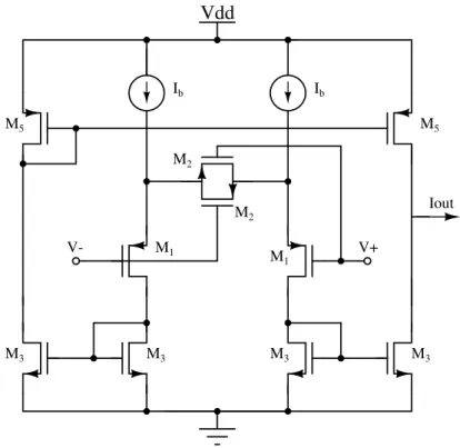
The first step was to use a 192nS OTA, taking advandage of the technique employed in [43] and [3], where current mirrors with a current scaling factor of m=0.3 are used in order to obtain such a transconductance. To achieve this current scaling, a 64nS OTA like shown in Fig. 5.3 was modified. Table3.6 shows the corresponding transistor dimensions.
Table 3.6: Unitary transistor dimensions for the OTAs.
Transistor W(µm) L(µm)
M1 0.8 7.2
M2 0.8 8
M3 5 2
M5 5 2
It must be pointed out that these trasistor dimensions are of unitary transistors, which are associated to form the transistors shown in Fig. 5.3. Thus, transistors M1 in Fig. 5.3, are
formed by the series association of 3 unitary transistors, the same applies to M3 and M5.
M2 is formed by series of 18 transistors.
Fig. 3.10, in section3.2.1 shows the 192nS OTA, with the current-scaling transistors added to the circuit. The modifications were made in the lower transistors, those named as M3 in
the figure. The bias current for this circuit is 20.16nA.
Current, transconductance and transient responses.
The following figures show the results from schematic simulation of the 192nS OTA. Fig.
3.17 shows the output current as a function a differential input voltage of ± 1V.
Vdd
Ib Ib
M5
M5
M2
M2
M1 V+
V-Iout
M3 M3 M3 M3
M1
Figure 3.16: Circuit schematic for a 64nS OTA.
−10 −0.8 −0.6 −0.4 −0.2 0 0.2 0.4 0.6 0.8 1
0.5 1 1.5 2 2.5
3x 10
−7
Tensión (V)
Corriente (A)
Figure 3.17: iout vrs Vd for the 192nS OTA.
−1 −0.8 −0.6 −0.4 −0.2 0 0.2 0.4 0.6 0.8 1
Figure 3.18: Transconductance curve of the 192nS OTA.
0.1 0.101 0.102 0.103 0.104 0.105 0.106 0.107 0.108 0.109 0.11 0
Figure 3.19: Output current transient response for the 192nS OTA.
Analog filter bank.
The original filter is shown in Fig. 3.14, in order to optimize its behavior the following changes were made: substitution of all of its OTAs and also its capacitances. The 385nS was changed by 192nS, and the 137nS, 68.5nS and 34.25 were changed by 64nS, 32nS and 16nS OTAs, respectively. Recalculation of capacitances was necesary as the filter bank had to maintain its cutoff frequencies. The required frequency response is the one shown in Fig. ??. Equation (3.8) was used to obtain these new capacitance values, where Gm is the
Table 3.7: Performance features of the 192nS OTA.
OTA Gmmax(nS) Cin (fF) Power (nW) ∆V(mV) SR (mV/µs)
transconductance of the OTA associated to the capacitor and fc the corresponding cutoff
frequency.
C = Gm 2πfc
(3.8)
Table 3.8 shows the capacitance values for the redesign filter. Shown cutoff frequencies are of every first order filter which conform each filter band. Every coefficient is generated by two first-order low pass filters and a first-order high pass filter at the output. The input filter is a first-order high pass followed by an amplification stage.
Table 3.8: Associated capacitance and Gm values in the filter bank.
Capacitor fc(Hz) Gm (nS) Capacitance (pF)
C1 875 64 12
Having the optimized OTAs and the new capacitance values, the filter structure shown in
3.20 was reimplemented.
The transfer function for each of the filter’s output coefficients is calculated. Coefficient 3 is shown in equation (3.9). This function has a second-order pole at 424Hz and a first-order pole at 845Hz.
CD3(s) =
sC3(64nS)2
(sC1 + 64nS)2(sC3 + 32nS) (3.9)
Equation (3.10) shows coefficient 4 with poles at 424Hz and 212Hz.
CD4(s) =
sC6(64nS)2
(sC4 + 64nS)2(sC6 + 32nS) (3.10)
_
Figure 3.20: Optimized filter bank diagram, where the OTA stages correspond to the optimization discussed in section 3.2.1.
CD5(s) =
sC9(16nS)(32nS)
(sC7 + 32nS)(sC8 + 16nS)(sC9 + 16nS) (3.11) Equation (3.12) shows the transfer function for the intemediate node.
V outN I(s) =
sC10(19264nSnS)
sC10 + 16nS (3.12)
Figs. 3.21 and 3.22 show the magnitud and phase frequency responses, respectively, both obtained from the theoretical transfer function.
100
100
Figure 3.22: Theoretical phase frequency response.
Biasing current mirrors
Every OTA in the filter works at a bias current of 20,16nA. Fig. 3.23 shows an instance of the current mirrors used to bias the whole filter, transistors M1 and M2 have the same size and their dimensions are: L=20µm and W=3µm.
Vdd
M1 M1 M1 M2 M2 M2
Iref I
copy
Figure 3.23: Current mirror biasing circuitry.
Schematic simulation results.
After the initial theoretical an´alisis, schematic driven simulations were carried out in order to assess the behavior of the optimized circuit. Fig. 3.24 shows the magnitude frequency response and Fig. 3.25the corresponding transient response. Fig. 3.26also shows a transient response but for several frequencies of the input signal.
100
(a) Frequency response for the intermediate node
(b) Frequency response for coefficient 3.
100 101 102 103 104 105
(c) Frequency response for coefficient 4.
100 101 102 103 104 105
(d) Frequency response for coefficient 5.
Figure 3.24: Magnitude frequency response for coefficients 3, 4, 5 and intermediate node.
0.1 0.1005 0.101 0.1015 0.102 0.1025 0.103 0.1035 0.104 0.1045
1.7
Figure 3.25: Filter transient response for an input of 600Hz of frequency.
As can be seen in table 3.10 the intermediate’s node capacitance was significantly reduced – a 90% – when compared to the original implementation reported in [9]. This helps in reducing the pole-shifting problem. As can be seen in Fig. 3.24, the highest value poles are
0.1 0.105 0.11 0.115 0.12 0.125 0.13 0.135 0.14 0.145 0.15
(a) Transient response to voltage input at 50Hz.
0.1 0.105 0.11 0.115 0.12 0.125 0.13
1.7
(b) Transient response to voltage input at 110Hz.
0.1 0.101 0.102 0.103 0.104 0.105 0.106 0.107 0.108 0.109 0.11 1.7
(c) Transient response to voltage input at 300Hz.
0.1 0.1002 0.1004 0.1006 0.1008 0.101 0.1012 0.1014 0.1016 0.1018 1.7
(d) Transient response to voltage input at 1500Hz.
Figure 3.26: Filter transient behavior for 100mV peak input at several frequencies.
shifted to the right due to the reduction of the size of the OTAs, which directly impact the gate capacitance. This capacitance is the main contributor to the intermediate node total capacitance. There are, however, differences in the higher frequency regions between theo-retical and schematic-driven simulation frequency responses. Nevertheless, in these regions the atenuation is so high that there is no effect on the desired behavior of the filter.
After optimization of the OTAs, the power consumption was 3.66µW, which represents a 34.29% reduction with regards to [9], without the need for current adjustments. See table
3.11.
Table 3.10: Filter’s obtained features vs initial ones.
Feature Initial Obtained values Improvement (%)
Power (µW) 5.57 3.66 34.29
Intermediate node capacitance (pF) 11.21 1.03 90.77
Table 3.11: Filter bank’s current consumption at 4V. IC implemented in [9].
Circuit Consumption with no adjustment (µA) Consumption with adjustment (µA)
Filter Bank 2.26 5.64
Table 3.12: Outputoffset voltage for the filter bank.
Stage offset Voltage (mV)
Coeficient 3 12.06
Coeficient 4 12.06
Coeficient 5 9.04
Intermediate node 68.06
Post layout filter results
Post-layout simulation results for the bank give a total power consumption of 7µW 4VVDD
supply, a third of what was reported in [9], but including 2µW dissipated on the three OpAmps connected as followers and placed at the output of each coefficient. These OpAmps (not shown in Fig. 3.20) are there only to minimize the effect of the capacitance of the pads in the filters’ response. Since these pads are mere measurement test points for this prototype, they would not be required in a final implementation, which means that the real power consumption ot the circuit should be around 5µW. The final area of the circuit is of 1.716 mm2. Fig. 3.15 shows the obtained frequency response.
3.2.3
Optimization of the computing unit.
The energy computing unit can be seen at the right-hand side in Fig. 3.9. It produces the sum of the rectified three coefficients computed by the filter (in this case, coefficients 3, 4 and 5, as shown in Fig. 3.29). In this case the goal is to have a detection stage with the lowest power consumption possible, while minimizing DC systematic offset that does not allow for a perfectly symmetrical rectification of each coefficient. This error could cause false gunshot detection (false alarms) which must be avoided. False detection not only lowers the detection efficiency, but causes wasted energy (a very limited resource) since it may imply the waking up of subsequent units of the WSN that verify the likelihood of the alarm. The optimized OTAs from the previous section will be reused here, such that the optimization problem is limited to other sections of the circuit.
Design of a two-stage comparator.
Fig. 3.27 shows a two-stage comparator that combines the features of the differential amplifier with the qualities of an inverter stage. The poor gain of the differential stage is increased by the gain of the inverter stage. The output of the differential stage, which is about VDD, is in the vicinity of the transition point of the inverter stage that follows.
Vdd
Figure 3.27: Schematic diagram for a two-stage comparator.
Comparator’s initial design and its implementation with an automated optimiza-tion tool.
As already stated, analog circuit dimensioning has the particularity that by varying some of its parameters will affect another of its characteristics. For example, when trying to re-duce the power consumption, the systematic offset or the duty cycle of the comparator can be adversely affected. This strong bond between parameters and performance makes it nec-essary to iterate in the design process to find an optimal compromise between the circuit’s requirements.
For comparison the initial design parameters of the comparator are used. These were ob-tained with hand made simulations, which are shown in Table 3.13. This step is not stricly necessary although it might help to have an acceptable starting point for the optimization process. Therefore, it was decided to try it that way. What it does matter is to have good circuit parameters’ constraints such that meaningful results can be obtained. A full discusion of a sizing rules methodology is given by Graeb in [27].
Table 3.13: Initial parameters for the comparator, with a bias current of 20µA
Transistor Dimensions W/L (µm)
M1 20/10
SR(i)=dVout(i)=
Vout(i+1)−Vout(i−1)
2d (3.13)
El valor de corriente de polarizaci´on y el consumo de potencia se obtienen directamente del archivo de simulaci´on. Finalmente, el offset se obtiene encontrando el valor de la tensi´on de entrada del comportamiento en CD para el cual la tensi´on de salida es igual a la referencia (en este casoV DD/2) y rest´andoselo a la referencia.
where i is the position in which the derivative is evaluated, Vout(i−1) and Vout(i+1) are the
voltage values before and after the evaluation, d is the time between two samples, 10µV as configured in the simulation environment is. The maximum rate of change from low to high and from high to low is obtained in order to choose the smallest value of both (the smallest being the worst case) as the correspongingslew rate.
The bias current value and the power consumption are obtained directly from the simulation output file. Finally, the offset is obtained by finding the value of the input voltage in the DC behavior in which the output voltage is equal to the reference (in this caseV DD/2) and then subtracting it from the reference.
Table 3.14: Comparator’s fitness values. Specification Fitness Value
Luego de los cambios realizados se simul´o de nuevo el comparador, obteni´endose el compor-tamiento de la figura3.28donde se aprecia la simetr´ıa del ciclo de trabajo, manteni´endose el offset sistem´atico por debajo de los 50µV con un consumo de potencia similar a lo obtenido de la simulaci´on en esquem´atico. El resumen de las caracter´ısticas post-layout se muestra en la tabla 3.15.
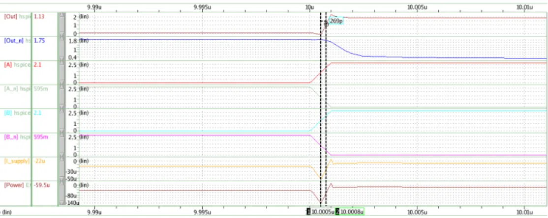
After these changes the comparator was simulated yielding the behavior of Fig 3.28, where the symmetry of the duty cycle can be appreciated, at the same time keeping the systematic offset below 50µ V with a power consumption similar to that obtained from the schematic simulation. Table3.15 presents a summary of the features from post-layout simulation.
Table 3.15: Comparator’s postlayout characteristics.
Offset (µV) Duty cycle (%) Ib (nA) Consumption (nA) @3,3V slew rate V /µs
35 49,9 14,5 35,4 401