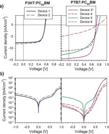
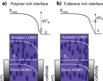
Charge carrier transport and contact selectivity limit the operation of PTB7 based organic solar cells of varying active layer thickness
Texto completo
Figure


Documento similar
The direction of the transport is regulated by the concentration of the substrates, ATPMg (or ADP) and phosphate. As phosphate uptake through the phosphate carrier is a very
The low thickness of the MAPbI 3 layer and the penetration of the MAPbI 3 in the NP layer guarantees that the majority of the photoinduced excitons or electron-hole
Therefore, the improvement of the device interfaces (increase of the thickness of MoSe 2 layer at the back and reduction of the GeSe 2 secondary phase at the front) and the
We have studied the dependence of the optical contrast with the flake thickness and the illumination wavelength of few-layer antimonene flakes on SiO 2 /Si substrates produced by
A reduced barrier layer thickness was revealed in the specimen anodised in the presence of molybdate, as a consequence of the increase of the resistance of the
In the previous sections we have shown how astronomical alignments and solar hierophanies – with a common interest in the solstices − were substantiated in the
In Figure 11(d), simulated red light illuminated IV curves are shown for acceptor-type defect states in the CdS and a conduction band spike at the CISe/CdS interface (model B1)
It is very interesting to observe in Figure S6 the impact on the back contact interface morphology when using monolayers (Mo 1 ) and bi-layers (Mo 2 ). The overselenization
