Electrodeposition and impedance spectroscopy characterization of ZnO nanowire arrays
7
0
0
Texto completo
(2) solidi. status. pss. physica. phys. stat. sol. (a) 205, No. 10, 2345 – 2350 (2008) / DOI 10.1002/pssa.200779426. a. www.pss-a.com. applications and materials science. Electrodeposition and impedance spectroscopy characterization of ZnO nanowire arrays R. Tena-Zaera*, 1, J. Elias1, C. Lévy-Clément1, I. Mora-Seró2, Y. Luo2, and J. Bisquert2 1 2. Institut de Chimie et Matériaux de Paris-Est, CNRS, UMR 7182, 94320 Thiais, France Departament de Física, Universitat Jaume I, 12071 Castelló, Spain. Received 16 October 2007, revised 9 June 2008, accepted 9 June 2008 Published online 25 July 2008 PACS 73.63.Nm, 81.05.Dz, 81.15.Pq, 82.45.Qr, 82.45.Vp *. Corresponding author: e-mail [email protected], Phone: +00 331 491 329, Fax: +00 331 491 203. An overview of the electrodeposition of ZnO nanowire arrays from the reduction of dissolved molecular oxygen in zinc chloride solutions was reported. In spite of the internal structure of ZnO which favours the anisotropic growth along the [0001] direction, the change in the local composition of the electrolyte around the nanowire during the electrodeposition was proposed as a major parameter to affect the nanowire growth mechanism. The influence of the ratio between the O2 reduction rate and the diffusion of Zn2+ to the cathode was emphasized. Due to the particular morphology of the nanowire arrays, no lateral growth was observed when the reduction of O2 was relatively fast, while the corresponding. deposition efficiency was very low. The decrease of the O2 reduction rate resulted in an enhancement of the deposition efficiency. The highest efficiencies (40 – 55%) were attained by using high chloride concentrations ([KCl] = 3.4 M) resulting not only in an enhancement of the longitudinal growth, but also in a considerable lateral growth. The influence of the electrodeposition conditions on the donor density of ZnO nanowires was investigated by using electrochemical impedance spectroscopy. Donor densities from 5 × 1019 cm–3 to 3 × 1020 cm–3 were obtained for as deposited samples. They decreased to values in the range of 1017 – 1018 cm–3 after annealing in air (1 hour at 450 °C).. © 2008 WILEY-VCH Verlag GmbH & Co. KGaA, Weinheim. 1 Introduction ZnO crystallizes in the wurzite structure (space group: C46v-P63mc) [1], presenting a charge asymmetry along ⟨0001⟩ axis [2]. Since this asymmetry favours the anisotropic growth along [0001] direction, ZnO nanowires oriented along ⟨0001⟩ axis have been obtained by several techniques such as vapour transport [3, 4], metalorganic chemical deposition [5], pulsed laser deposition [6], chemical bath deposition [7] and electrochemical deposition [8]. In recent years single-crystal ZnO nanowire arrays have emerged as promising building blocks for a new generation of devices in different technological domains such as optoelectronics [9, 10], solar cells [11, 12], gas sensing [13, 14], field emission [15, 16], piezoelectrics [17] and microfluidics [18]. Once the potential of single crystal ZnO nanowires in nanostructured devices has been shown, further investigations were required to enhance their performances. The dimensions and electrical properties of ZnO nanowires appear. to be major parameters for the optimization of most of the above mentioned devices (e.g. [14, 15, 19]). Electrodeposition is a low temperature technique well suited for cheap large-scale production process. Besides, electrodeposited ZnO nanowire arrays have already shown great potentiality in nanostructured solar cells [12], electroluminescent hybrid light emitting diodes [10] and microfluidics [18]. ZnO one-dimensional nanostructures can be electrode– posited from the reduction of NO3 [20, 21], H2O2 (using templates) [22, 23] and O2 [24]. The latest method appears to be the best option for the controlled electrodeposition of ZnO nanowire arrays and for the tailoring of their dimensions [25–28]. Some of the reported strategies proposed to tune the nanowire dimensions are based on the variation of the ratio between the concentrations of oxygen and zinc precursors and/or on the use of adsorbing anions, which may also affect the electrical properties of the ZnO nanowires. © 2008 WILEY-VCH Verlag GmbH & Co. KGaA, Weinheim.
(3) 2346. solidi. status. physica. pss. a. R. Tena-Zaera et al.: Electrodeposition and impedance spectroscopy of ZnO nanowire arrays. The particular morphology of nanowire arrays makes their electrical characterization difficult. Very recently several methods employing impedance spectroscopy have been developed to determine donor density of ZnO nanowire arrays [19, 29]. The electrochemical impedance spectroscopy, establishing a semiconductor/liquid junction, presents the advantage that it is a non-destructive method and no-solid contact is needed as backcontact [19]. Here, we present a general discussion about the growth mechanism of electrodeposited ZnO nanowires, emphasizing the influence of the O2 reduction rate versus the diffusion of Zn2+ to the cathode. The influence of the electrochemical deposition conditions on the electrical properties of the ZnO nanowires is also analyzed by using electrochemical impedance spectroscopy. 2 Experimental The electrodeposition (ECD) of ZnO nanowire arrays was performed in a three-electrode electrochemical cell with the substrate as the cathode, a Pt spiral wire as the counter electrode and a Saturated Calomel Electrode (SCE) as the reference electrode. The electrolyte was an aqueous solution of ZnCl2 and KCl, saturated with bubbling oxygen. Ultrapure water (18 MΩ cm) was provided by a Millipore setup. ZnCl2 salt (Flucka, purity >98.0%) was the Zn2+ precursor and its concentration was 5 × 10⁻⁴ M. KCl (Flucka, purity >99.5%) acted, among other roles, as a supporting electrolyte. Its concentration was 0.1 M and 3.4 M for “low” and “high” chloride concentrations, respectively. The substrates were commercial conducting (10 Ω/ square) glass/SnO2 :F, from Solaronix, covered by a thin continuous layer of ZnO deposited by spray pyrolysis at ∼350 °C. Experimental details about the deposition of ZnO sprayed layer can be found elsewhere [28]. For each working electrode, a geometric surface of 2 cm2 was masked off prior to the electrodeposition experiments. Then, on top of the sprayed ZnO buffer layer, the ZnO nanowire arrays were electrodeposited at 80 °C under constant potential (–1 V vs. SCE) or under constant current density (–0.32 mA/cm2). Two different charge densities (2.5 and 10 C/cm2) were used. Cyclic voltammetry (CV) experiments were performed at 80 °C. Two scans for each sample were carried out from solution rest potential (near zero), with a cathodic sweep to –1.5 V vs. SCE and followed by an anodic sweep to +0.5 V vs. SCE. Scan rate was 10 mV/s. The electrochemical impedance spectroscopy (EIS) measurements were performed in a three-electrode cell using a Pt wire as counter electrode and a standard Ag/AgCl in 3 M KCl as reference electrode. A carbonate propylene electrolyte (0.1 M LiClO4) was used to avoid ZnO decomposition. Each measurement was done applying a 20 mV AC sinusoidal signal over the constant applied bias with the frequency ranging between 500 kHz and 5 mHz. After the electrochemical measurement, the as deposited samples were annealed in air at 450 °C for 1 hour at atmospheric pressure, followed by cooling in ambient air. © 2008 WILEY-VCH Verlag GmbH & Co. KGaA, Weinheim. ECD, CV experiments and EIS data were obtained using an Autolab PGSTAT-30 with a frequency analyzer (FRA) in the case of EIS. 3 Results and discussion 3.1 Electrodeposition The electrochemical reduction of O2 occurs by a two (Eq. (1)) or a four (Eq. (2)) electron process, as a function of the electrolyte and cathode properties [30, 31] O2 + 2H2O + 2e– → H2O2 + 2OH– , –. –. O2 + 2H2O + 4e → 4OH .. (1) (2). The generation of hydroxide ions induces an increase of the local pH close to the cathode. Zn2+ and OH– ions react together leading to the formation of ZnO and its deposition on the surface of the cathode (Eq. (3)) [24] Zn2+ + 2OH– → ZnO + H2O .. (3). Although the internal structure of ZnO favours the anisotropic growth along the [0001] direction [32], the surrounding conditions during the deposition may affect the growth mechanism of the ZnO nanowires. Since ZnO formation has generally a fast kinetics, the local composition of the electrolyte around the nanowires will be mainly determined by the ratio between the rate of OH– generation and the diffusion of Zn2+ ions to the cathode. Figure 1 summarizes the schematic view of the three extreme situations for the electrodeposition of ZnO nanowire arrays. Figure 1a corresponds to an OH– production much faster than the Zn2+ diffusion. Figure 1c represents the opposite situation and Fig. 1b shows the scenario when the OH– production rate and the Zn2+ diffusion are similar. The particular morphology of the nanowire arrays makes that the lateral growth can only occur when the rate of the OH– generation and the Zn2+ diffusion rate are similar (Fig. 1b). Even in this scenario, an enhancement of the longitudinal growth rate is expected due to the internal structure of ZnO [32]. However, the use of adsorbing species as selective ZnO face stabilizers has been proposed to act on the ratio between the longitudinal and the lateral growth rates [20, 26, 33]. A very low deposition efficiency, defined as the ratio between the OH– that react with Zn2+ (yielding ZnO, Eq. (3)) and the total amount of OH– produce from O2 electroredution (Eqs. (1) and/or (2)), is predicted for the scenario of Fig. 1a. However, the deposition efficiency should increase for the scenario of Fig. 1b, reaching the highest values for the case of Fig. 1c. The electrodeposition of ZnO nanowire arrays reported in our previous work (V = –1 V vs. SCE, [ZnCl2] = 5 × 10⁻⁴ M, [KCl] = 0.1 M and T = 80 °C) seems to be close to the scenario of Fig. 1a because no significant lateral growth was observed and a deposition efficiency of ∼5% was estimated [27]. Considering these electrodeposition conditions as a reference, there are several ways to act www.pss-a.com.
(4) Original Paper phys. stat. sol. (a) 205, No. 10 (2008). 2347. 0.0. 2. J (mA/cm ). C B. -0.5. A -1.0. [KCl] = 0.1 M [KCl] = 3.4 M -1.5 -1.5. -1.0 -0.5 V vs. SCE (V). 0.0. Figure 2 (online colour at: www.pss-a.com) Cathodic current – potential scans of SnO2 : F electrode in deposition solutions (O2 saturated, [ZnCl2] = 5 × 10⁻⁴ M) with two different KCl concentration (empty squares: 0.1 M and filled squares: 3.4 M).. as A, B and C in the text. Two different charge densities were used for each condition to analyze the evolution of nanowire dimensions as a function of the charge. Figure 3 summarizes the SEM micrographs of the obtained ZnO nanowire arrays. A large decrease of the nanowire density can be inferred for the arrays deposited under conditions C, especially those obtained after passing 10 C/cm2. As discussed in detail in Ref. [27], the growth of the most vertical nanowires is favoured against that of the tilted ones, in-. Figure 1 (online colour at: www.pss-a.com) Schematic view of the growth of the electrodeposited ZnO nanowires when: a) the OH– generation rate is much faster than the Zn2+ diffusion, b) the OH– generation rate is similar to the Zn2+ diffusion and c) the OH– generation much slower than the Zn2+ diffusion. The arrows indicate the growth direction.. on the growth mechanism of ZnO nanowires, by modifying the generation rate of OH–. They are discussed in the following. Figure 2 summarizes the cathodic forward sweeps of CV performed on conducting glass substrates in two different deposition solutions ([KCl] = 0.1 M and 3.4 M). The CV have been discussed in detail elsewhere [26]. Here, we only use Fig. 2 to show two different ways to decrease the OH– generation rate. The simplest one is to perform the electrodeposition using identical solution, but at lower current density (point B instead of A, Fig. 2). An alternative option to decrease the OH– generation rate is by using higher chloride concentrations [26, 31] (point C of Fig. 2). In order to check the validity of the discussion, electrodepositions under different conditions (points A, B and C of Fig. 2) were performed. These conditions are referred www.pss-a.com. Figure 3 SEM micrographs of the ZnO nanowire arrays obtained for A conditions: a) 2.5 and b) 10 C/cm2, B conditions: c) 2.5 and d) 10 C/cm2 and C conditions: e) 2.5 and f) 10 C/cm2. © 2008 WILEY-VCH Verlag GmbH & Co. KGaA, Weinheim.
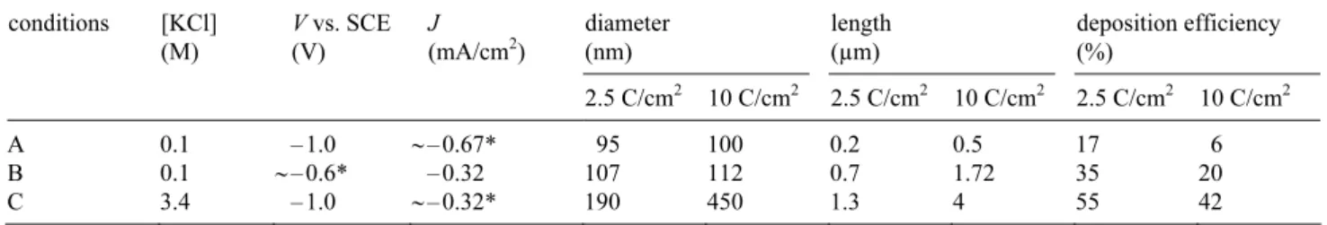
(5) solidi. status. physica. pss. 2348. a. R. Tena-Zaera et al.: Electrodeposition and impedance spectroscopy of ZnO nanowire arrays. Table 1 Diameter, length and deposition efficiency for the A, B and C electrodeposition conditions. conditions. A B C. [KCl] (M). 0.1 0.1 3.4. ∼ V vs. SCE ∼ J ∼ (V) ∼ (mA/cm2). ∼ – 1.0 ∼ – 0.6* ∼ – 1.0. ∼ – 0.67* ∼ – 0.32 ∼ – 0.32*. diameter (nm). length (µm). deposition efficiency (%). 2.5 C/cm2. 10 C/cm2. 2.5 C/cm2. 10 C/cm2. 2.5 C/cm2. 10 C/cm2. 95 107 190. 100 112 450. 0.2 0.7 1.3. 0.5 1.72 4. 17 35 55. 6 20 42. * Steady-sate values obtained when the other parameter (V or J) was fixed.. ducing a selective process during the electrodeposition experiment. This is illustrated in Fig. 3f where the array is constituted of the longest nanowires. The lowest density can be observed for this sample. Thus, the variation of the nanowire density inferred in plan view SEM images is mainly due to the differences in the length of the nanowires and not to the differences in the electrodeposition conditions. The mean values of the nanowire dimensions and deposition efficiency, estimated by weighing numerous samples before and after the electrodeposition, corresponding to the A, B and C conditions are summarized in Table 1. Only small differences (∼5 nm) in nanowire diameter are observed between the samples obtained after passing 2.5 C/cm2 and 10 C/cm2 for the A and B deposition conditions ([KCl] = 0.1 M). On the contrary, for the C conditions ([KCl] = 3.4 M) the nanowire diameter increases by a factor larger than 2 by passing 10 instead of 2.5 C/cm2. The nanowire length increases as a function of the charge density for the three different electrochemical con ditions (A, B and C). Most interestingly, for a constant charge density the length of the nanowires increases from A to B and then to C conditions. Irrespective of the electrodeposition conditions, the deposition efficiency decreases as a function of the charge density (Table 1). This is due to the selective deposition process that results in a decrease of the nanowire density on the top of the array and, therefore, in a decrease of the deposition efficiency as the nanowire length increases. By comparing the nanowire dimensions and the deposition efficiency obtained for the A and B conditions ([KCl] = 0.1 M), we can conclude that the major effect of decreasing the current density is to enhance the deposition efficiency. This is due to the decrease of the OH– generation rate versus the Zn2+ diffusion, which mainly results in an enhancement of the longitudinal growth rate. However, the lateral growth seems to be limited to the first growth stages, when the nanowire morphology is not yet developed [27], for both studied current densities (–0.67 mA/cm2 and –0.32 mA/cm2). Since the current density of the B and C conditions was the same, the comparison between the obtained nanowire arrays (Fig. 3c–f) may be used to get a further insight into the role of chloride anions on the growth of ZnO nanowires. The role of Cl– ions as stabilizers of the (0001) © 2008 WILEY-VCH Verlag GmbH & Co. KGaA, Weinheim. ZnO surface, evoked in the Refs. [20, 26], might be the origin of the lateral growth observed for “high” chloride concentrations (Fig. 3e and f). However it cannot explain the enhancement of the longitudinal growth. Other authors have reported that the presence of Cl– modifies the oxygen reduction mechanism on metallic substrates such as silver [34] and nickel [31], inducing the formation of H2O2 as an intermediate species by a twoelectron reduction process (Eq. (1)) instead of a direct four-electron process (Eq. (2)). Lincot’s group [35] has recently studied O2 electroreduction on ZnO electrodes, finding that the total number of exchanged electrons during O2 reduction is ∼3.4 for [KCl] = 0.1 M. This may indicate that a four-electron process is dominant under these conditions. Nevertheless, the two-electron process may become more important when [Cl–] increases due to the adsorption of chloride ions on the ZnO surfaces [36]. This effect appears as one of the most probable origins of the decrease of current density for “high” chloride concentrations (Fig. 2). However, the decrease of the solubility of O2 in aqueous solutions as a function of the chloride concentration [37] may also contribute to the current decrease. Since the kinetics of O2 reduction by a two-electron process (Eq. (1)) is lower than those of the direct fourelectron pathway (Eq. (2)) [38], although the current density was the same for the B and C deposition conditions (Fig. 2), the slowest OH– generation is expected for “high” chloride concentrations. As a consequence, the deposition efficiency is enhanced for the C deposition conditions. Contrarily to “low” chloride concentrations, its increase results not only in the longitudinal growth, but also in the lateral one. This suggests that the growth of ZnO nanowire arrays occurs in a scenario similar to that of Fig. 1b. As previously discussed, chloride ions can be adsorbed on (0001) ZnO surface decreasing the ratio between the longitudinal and the lateral growth rate. Thus, the use of high chloride concentrations appears to be an efficient way to act on the growth mechanism of the electrodeposited ZnO nanowires shifting from scenario of Fig. 1a to that of Fig. 1b. 3.2 Electrochemical impedance spectroscopy The electrical behaviour of the nanowire arrays obtained using “low” and “high” chloride concentrations was analyzed by electrochemical impedance spectroscopy. A Mott– Schottky (MS) model that takes into account the particular www.pss-a.com.
(6) Original Paper phys. stat. sol. (a) 205, No. 10 (2008). 2349. Figure 4 (online colour at: www.pss-a.com) a) Capacitance and b) Mott – Schottky plots of as deposited ZnO nanowire arrays and after thermal annealing, for two different KCl concentrations (0.1 M and 3.4 M).. morphology of the nanowire arrays, was developed to determine the carrier density in electrodeposited ZnO samples. The details of the model can be found elsewhere [19]. Briefly, the method is an extension of the Mott–Schottky (MS) analysis commonly used to determine both dopant density and flatband potential at flat semiconductor and semiconductor/liquid junctions, but taking into account the particular geometry of ZnO nanowires. The nanowire capacitance was obtained from the impedance spectra. The donor density was determined by fitting the capacitance in the range of voltages where it is governed by the size of the depletion region. The capacitances and MS plots of the samples obtained for the A and C deposition conditions ([KCl] = 0.1 M and 3.4 M, respectively) are shown in Fig. 4. Data of the same samples after annealing in air (1 hour at 450 °C) are also plotted in Fig. 4. Solid lines represent the fits of the experimental data employing the model of the Ref. [19]. A very good agreement between the experimental data and the model is observed at reverse bias, except for potentials higher than 0.8 V vs. Ag/AgCl, where the capacitance from the buffer layer may become predominant [19]. For as deposited samples, which present high donor density, MS plot (Fig. 4b) presents a linear behaviour very close to that typically observed in flat samples [39]. Nevertheless Table 2 Donor density (Nd) of the nanowires obtained for A and B electrodeposition conditions. deposition conditions A C. [KCl] (M) 0.1 3.4. * 1 hour at 450 °C in air. www.pss-a.com. Nd (cm–3) as deposited. annealed*. 5 × 10 3 × 10²⁰. 2 × 10¹⁸ 5 × 10¹⁷. 19. the special geometry of the samples has to be taken into account to avoid errors in the determination of donor density. For samples with lower donor density (as deposited samples) a curved MS plot is obtained and the effect of the nanowire morphology is clearly manifested. Table 2 shows the obtained values for the donor density of ZnO nanowires. For the as deposited nanowires, the donor density increases for “high” chloride concentration. On the contrary, after annealing, the donor density is higher for nanowires deposited using low “chloride” concentrations. As discussed in the previous section, the use of “high” chloride concentration results in a decrease of the OH– generation rate. This induces an increase of the [Zn2+]/[OH–] ratio close to the cathode. Since the energy formation of ZnO intrinsic defects with an electrical donor behavior, such as oxygen vacancies (VO) or zinc atoms in interstitials positions (Zni) decreases in zinc rich conditions [40, 41], the increase of the [Zn2+]/[OH–] ratio may result in a higher amount of donor defects in ZnO nanowires. This could explain the increase of the donor density in the as deposited samples for “high” chloride concentrations. The concentration of intrinsic donor defects should decrease after annealing in air, giving more relevance to the electrical role of Cl impurities, whose content is expected to be increased with [KCl]. Chlorine can be adsorbed onto the nanowire surface or placed into the bulk. In the latter case the electrical role depends on their position into the ZnO lattice. Chlorine impurities may act as electrical donors if they substitute oxygen atoms. However, they may present an acceptor behavior if they are in interstitial position or form some complexes with some intrinsic ZnO defects [42]. Because the donor density of annealed samples decreases with [KCl], compensation effect due to the presence of chlorine related defects with a net negative charge state is suggested. Complementary studies are now undertaken to gain a further insight into the position and the role of Cl atoms on the electrical properties of ZnO nanowires. 4 Conclusion A general discussion about the influence of the surrounding conditions on the growth mechanism of the electrodeposited ZnO nanowires was reported. The effect of the ratio between the O2 reduction rate and the diffusion of Zn2+ to the cathode has been emphasized. Due to the particular morphology of the nanowire arrays, when the reduction of O2 is relatively fast the deposition efficiency is very low and no lateral growth occurs. However, the decrease of the O2 reduction rate results in an enhancement of the deposition efficiency. Values in the range of 40–55% have been attained by using high chloride concentrations ([KCl] = 3.4 M), inducing a considerable lateral growth. The general discussion not only enhances the understanding about the growth mechanism of ZnO nanowires electrodeposited from O2 reduction, but also opens new approaches for other (electro)chemical methods based on solution techniques. On the other hand, the influence of the deposition conditions on the electrical properties of the © 2008 WILEY-VCH Verlag GmbH & Co. KGaA, Weinheim.
(7) solidi. status. physica. pss. 2350. a. R. Tena-Zaera et al.: Electrodeposition and impedance spectroscopy of ZnO nanowire arrays. ZnO nanowires has been also studied by using electrochemical impedance spectroscopy. Donor densities from 5 × 10¹⁹ to 3 × 1020 cm–3 have been obtained for as deposited samples. However, air annealed samples (1 hour at 450 °C) exhibit values in the range of 1017 –1018 cm–3. Acknowledgements The work was partially supported by Ministerio de Educación y Ciencia of Spain under project MAT2004-05168 and Generalitat Valenciana under the project GV06/347.. References [1] O. Madelung, Semiconductors Basic Data (Springer Verlag, Berlin, 1996). [2] C. Noguera, J. Phys.: Condens. Matter. 12, R367 (2000). [3] M. Huang, Y. Wu, H. Feick, N. Tran, E. Weber, and P. Yang, Adv. Mater. 13, 113 (2001). [4] Y. Ding, P. X. Gao, and Z. L. Wang, J. Am. Chem. Soc. 126, 2066 (2004). [5] W. I. Park, D. H. Kim, S. W. Jung, and G. C. Yi, Appl. Phys. Lett. 80, 4232 (2002). [6] J. Zuniga-Perez, A. Rahm, C. Czekalla, J. Lenzner, M. Lorenz, and M. Grundmann, Nanotechnology 18, 195303 (2007). [7] L. Vayssieres, Adv. Mater. 15, 464 (2003). [8] R. Könenkamp, K. Boedecker, M. C. Lux-Steiner, M. Poschenrieder, F. Zenia, C. Levy-Clement, and S. Wagner, Appl. Phys. Lett. 77, 2575 (2000). [9] W. I. Park and G. C. Yi, Adv. Mater. 16, 87 (2004). [10] R. Konenkamp, R. C. Word, and M. Godinez, Nano Lett. 5, 2005 (2005). [11] M. Law, L. E. Greene, J. C. Johnson, R. Saykally, and P. Yang, Nature Mater. 4, 455 (2005). [12] C. Lévy-Clément, R. Tena-Zaera, M. A. Ryan, A. Katty, and G. Hodes, Adv. Mater. 17, 1512 (2005). [13] L. C. Tien, P. W. Sadik, D. P. Norton, L. F. Voss, S. J. Pearton, H. T. Wang, B. S. Kang, F. Ren, J. Jun, and J. Lin, Appl. Phys. Lett. 87, 222106 (2005). [14] L. Liao, H. B. Lu, J. C. Li, H. He, D. F. Wang, D. J. Fu, C. Liu, and W. F. Zhang, J. Phys. Chem. C 111, 1990 (2007). [15] C. Ye, Y. Bando, X. Fang, G. Shen, and D. Goldberg, J. Phys. Chem. C 111, 12673 (2007). [16] X. Wang, J. Zhou, C. Lao, J. Song, N. Xu, and Z. L. Wang, Adv. Mater. 19, 1627 (2007). [17] X. Wang, J. Song, J. Liu, and Z. L. Wang, Science 316, 102 (2007).. © 2008 WILEY-VCH Verlag GmbH & Co. KGaA, Weinheim. [18] C. Badre, T. Pauporté, M. Turmine, and D. Lincot, Nanotechnology 18, 365705 (2007). [19] I. Mora-Sero, F. Fabregat-Santiago, B. Denier, J. Bisquert, R. Tena-Zaera, J. Elias, and C. Lévy-Clément, Appl. Phys. Lett. 89, 203117 (2006). [20] L. Xu, Y. Guo, Q. Liao, J. Zhang, and D. Xu, J. Phys. Chem. B 109, 13519 (2005). [21] Q. P. Chen, M. Z. Xue, Q. R. Sheng, Y. G. Liu, and Z. F. Ma, Electrochem. Solid State Lett. 9, C58 (2006). [22] M. Lai and D. J. Riley, Chem. Mater. 18, 2237 (2006). [23] Y. Leprince-Wang, G. Y. Wang, X. Z. Zhang, and D. P. Yu, J. Cryst. Growth 287, 89 (2006). [24] S. Peulon and D. Lincot, J. Electrochem. Soc. 145, 864 (1998). [25] R. Tena-Zaera, A. Katty, S. Bastide, C. Lévy-Clément, B. O’Regan, and V. Muñoz-Sanjosé, Thin Solid Films 483, 372 (2005). [26] R. Tena-Zaera, J. Elias, G. Wang, and C. Lévy-Clément, J. Phys. Chem. C 111, 16706 (2007). [27] J. Elias, R. Tena-Zaera, and C. Lévy-Clément, J. Electroanal. Chem. (2007) in press (http://dx.doi.org/10.1016/ j.jelechem.2007.09.015). [28] J. Elias, R. Tena-Zaera, and C. Lévy-Clément, Thin Solid Films 515, 8553 (2007). [29] J. J. Wu and D. K.-P. Wong, Adv. Mater. 19, 2015 (2007). [30] S. Strbac and R. R. Adzic, Electrochim. Acta 41, 2903 (1996). [31] S. P. Jiang, C. Q. Cui, and A. C. C. Tseung, J. Electrochem. Soc. 138, 3599 (1991). [32] W. J. Li, E. W. Shi, W. Z. Zhong, and Z. W. Yin, J. Cryst. Growth 203, 186 (1999). [33] T. Yoshida, M. Tochimoto, D. Schlettwein, D. Wohrle, T. Sugiura, and H. Minoura, Chem. Mater. 11, 2657 (1999). [34] E. Brandt, J. Electroanal. Chem. 150, 97 (1983). [35] A. Goux, T. Pauporté, and D. Lincot, Electrochim. Acta 51, 3168 (2006). [36] J. Elias, R. Tena-Zaera, and C. Lévy-Clément, J. Phys. Chem. C 112, 5736 (2008). [37] Handbook of Chemistry and Physics, 69th ed. (Chemical Rubber Publishing Company, Boca Raton, 1988), p. D-272. [38] W. E. Mustain and J. Prakash, J. Electrochem. Soc. 154, A668 (2007). [39] S. M. Sze, Physics of Semiconductor Devices, 2nd ed. (John Wiley and Sons, New York, 1981), p. 79. [40] S. B. Zhang, S. H. Wei, and A. Zunger, Phys. Rev. B 63, 75205 (2003). [41] A. F. Kohan, G. Ceder, D. Morgan, and C. G. Van de Walle, Phys. Rev. B 61, 15019 (2000). [42] T. Tchelidze, E. Chikoidze, O. Gorochov, and P. Galtier, Thin Solid Films 515, 8744 (2007).. www.pss-a.com.
(8)
Figure
![Figure 2 summarizes the cathodic forward sweeps of CV performed on conducting glass substrates in two dif-ferent deposition solutions ([KCl] = 0.1 M and 3.4 M)](https://thumb-us.123doks.com/thumbv2/123dok_es/3361905.606195/4.892.86.285.158.731/figure-summarizes-cathodic-performed-conducting-substrates-deposition-solutions.webp)

Documento similar
· En el artículo “Characterization of macadamia and pecan oils and detection of mixtures from other edible seed oils by Raman spectroscopy” se caracterizan por Raman
Micromagnetic simulations of magnetization reversal of various Co nanowires with different aspect ratios (from 120 to 1000 nm in length, and 35 to 75 nm diameter) were
Of special concern for this work are outbreaks formed by the benthic dinoflagellate Ostreopsis (Schmidt), including several species producers of palytoxin (PLTX)-like compounds,
Through this manuscript was presented the behaviour of different compositions of metal- lic glasses as a response to an additional variable, namely pressure for the analysis
Characterization of the thermal contacts between heat exchangers and a thermoelectric module by impedance spectroscopy (under
In summary, the ability to perform a complete characterization of all TE properties of a bulk material as a function of temperature, from a single electrical impedance
Impedance spectroscopy measurements were carried out on the fillers and mixed matrix membranes (MMM) in wet conditions (ZIFsTW and PZIFsTW) and dry conditions (ZIFsTD and PZIFsTD)
Using a combination of optical photometry and spectroscopy we esti- mate stellar masses, ages, and foreground extinction values of the brightest part of the population
