1
Single ADC Digital PFC Controller using
Pre-calculated Duty Cycles
Alberto Sanchez, Angel de Castro, Member, IEEE, Victor M. L´opez, Student Member, IEEE,
Francisco J. Azcondo, Senior Member, IEEE, and Javier Garrido, Senior Member, IEEE
Abstract—Traditional digital PFC (Power Factor Correction) uses three sensors to measure the input and output voltages and the input current. Each sensor, especially the input current one, increases the cost of the system and generates power losses in case of resistive sensors. This paper presents a controller for boost PFC converters. It uses pre-calculated duty cycles generated offline, and applies them to the switch. In order to control the converter with non-nominal conditions, just one ADC (Analog to Digital Converter) is used, which measures the output voltage. Measuring the average and the ripple of the output voltage with this ADC, the controller takes compensation action for changes in the input voltage but also in the load of the converter. The average value is used to control the input voltage changes, whilst the ripple value is used to control load changes. These two loops present low frequency bandwidth, so the ADC and the whole system can be low cost. Finally, a comparator is used to detect the zero-crossing of the input voltage, so the pre-calculated values are synchronized with the ac mains. In this way, the converter only uses one ADC and one comparator, both with low bandwidth. Results show that high power factor and normative compliance are reached, even under non-nominal conditions.
Index Terms—rectifiers, digital control, switched mode power supplies, field programmable gate arrays.
I. INTRODUCTION
C
LASSIC PFC techniques usually need to sense the input and output voltages, and the input current. Sensing the input current is not a trivial issue. It is a common practice to utilize a resistive sensor, but it generates power losses and hot that must be evacuated. Besides, in the case of digital control, the voltage through the resistor should be digitized with an ADC and the input current frequency is equal to the switching frequency. Hence, this ADC should have higher sampling frequency than the ADCs used for the input and output voltages, which change at the line frequency and can be low cost ADCs.Taking advantage of digital techniques, many proposals avoiding current sensing have been presented. Some of them utilize current estimation using voltage ADC measurements [1]–[3]. These proposals were applied to dc-dc multiphase converters. [4] presents an input current estimation method measuring the inductor voltage also for dc-dc converters.
For PFC, this is even more critical, because in the general case three ADCs are necessary. In [5], a fully digitalized
Mr. Alberto Sanchez, Dr. Angel de Castro and Dr. Javier Garrido are with the HCTLab laboratory. Univ. Autonoma de Madrid. Francisco Tomas y Valiente 11, 28049 Madrid, Spain (email: {alberto.sanchezgonzalez, an-gel.decastro, javier.garrido}@uam.es)
Mr. Victor M. L´opez and Dr. Francisco J. Azcondo are with the Department of Electronics Technology System and Automation Engineering. University of Cantabria, 39005 Santander, Spain (email: {lopezvm, azcondof}@unican.es)
PFC rectifier is proposed without any ADC. The three typical variables are measured, but using comparators and saw-tooth signals, avoiding ADCs. In [6], the variable which is not measured is the input voltage, but most works focus on obtaining PFC without measuring the input current [7]–[14]. For instance, in [7] a PFC boost converter is presented. In that proposal, the input current is not measured but its zero crossing is detected measuring the input and output voltages. In [8], [9], a current estimation method also using input and output voltage measures from low cost ADCs is presented. [10] describes a PFC converter which only uses a voltage loop, avoiding the current loop. That system achieves good performance at nominal input conditions and even under transients. The same authors presented a modification of the algorithm [11] which improves the results under distorted input voltage, but it also increases the complexity of the system.
Other way of avoiding current measurement in PFC is to pre-calculate the duty cycle for a line period in nominal conditions, and start applying those pre-calculated values when a zero-crossing is detected [12]–[15]. However, the power factor quickly decreases under conditions not exactly equal to nominal ones if no compensation is applied.
[12], [13] present a pre-calculated method and its online control when the output voltage changes due to the load. This control only selects which set of duty cycles is output from eight possible sets and no input voltage changes are considered.
Besides, in [14], a predictive process calculates the duty cycles of the next ac line period measuring the input and output voltages of the present ac period. That system presents limitations in case of load changes. The same authors present an improved system in [15], which reduces the limitations of the previous proposal. However, it also measures the input current, increasing the cost of the system.
This work presents a method to pre-calculate offline the duty cycles which are applied to the PFC switching converter. A deep analysis of the duty cycle is presented and it is divided into three components. Besides, several methods to regulate them online, in case of non-nominal conditions, are presented. The aim of this work is to reduce the cost of the PFC system. Previous proposals decrease the number of ADCs from three to two. In this proposal, a single ADC for the output voltage is used. However, in order to obtain two control loops, both the mean output voltage and its ripple are measured. In this way, the system is able to compensate for the changes in the input voltage but also in the load of the converter. Finally, only a comparator is used for synchronization (zero-crossing
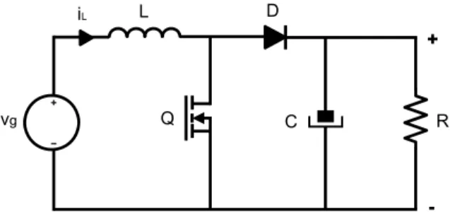
vg iL D Q C R + -L
Fig. 1. Boost converter used for PFC
detection) with the ac mains, but no ADC for the input voltage nor the input current.
The rest of the paper is organized as follows. Section II defines how to pre-calculate the duty cycles of the PWM which will be applied to the switch of the power converter. Section III defines several control techniques which are used to make the system robust in case of input changes. Section IV shows the experimental results of all the presented techniques. Finally, conclusions are given in section V.
II. PRE-CALCULATED DUTY CYCLE VALUES
In a PFC system, the switch of the converter can be controlled by a digital PWM with variable duty cycle. The values of the duty cycle are usually controlled sensing the input voltage and current and the output voltage. In this paper, the duty cycles are pre-calculated in advance and stored in a memory, so no calculus is necessary during run-time. These values are specific for each design. The system will apply the duty cycles to generate the PWM switching signal. The main advantage of using pre-calculated duty cycles is to avoid sensors. Ideally, only synchronization with the utility would be necessary. However, compensators must be implemented to work under not exactly nominal conditions, so additional sensors are needed. As it will be shown in section III, with the proposed pre-calculated technique only the output voltage sensor is necessary.
The calculus of the duty cycles depends on the topology of the converter, which is a boost converter in our case (Fig. 1). This paper shows the calculus only for a boost converter op-erating at CCM and under sinusoidal input voltage. However, it would be similar with other topologies. The equation of the inductor is analyzed when the inductor is charging (switch on) and discharging (switch off):
vLON = vg = L · diL dt vLOF F = vg− vout= L · diL dt (1) where L is the inductance, vg is the input voltage and vout
the output voltage. The system of equations (1) is discretized and translated into a difference equation and it is solved for iL: iL(k + 1) = iL(k) + ∆iLON + ∆iLOF F = iL(k) + vg(k) L · TSw· d(k) + +vg(k) − vout(k) L · TSw· (1 − d(k)) (2)
where k indicates the switching cycle inside an input ac period, TSw is the switching period which is constant, and d
is the duty cycle, normalized to unity, which will be applied to the switch. Therefore, TSw· d(k) is the time of charging,
and TSw· (1 − d(k)) the time of discharging. The input current
of each step depends on the previous current value, the input and output voltages, and the present duty cycle. The equation (2) is solved for the duty cycle obtaining:
d(k) = vout(k) − vg(k) vout(k) + + L TSw · (iL(k + 1) − iL(k)) vout(k) (3) This equation generates the duty cycle for each switching period inside a rectified ac period. These duty cycles can be applied periodically so, for instance, if the rectified utility period is divided into 1 000 switching cycles, then only 1 000 values should be stored into a memory. The variable vout(k)
represents the output voltage in the switching period k. The output voltage has a ripple component produced by the load:
voutRipple(k) =
Pout
C · 2ωr· Vout
· sin(2 · ωr· kTsw) (4)
Pout is the mean output power, C the capacitance of the
output capacitor, and ωris angular frequency of the ac mains.
As seen in (4), the frequency of the output voltage ripple is twice the frequency of the ac mains. Therefore, vout(k) in (3)
corresponds to:
vout(k) = Vout− voutRipple(k) (5) Besides, the input current (iL) can be calculated knowing
that it is a periodic variable which depends on the power that the load demands and the input voltage:
iL(k) =
Pg
Vg
·√2 · sin(ωr· kTsw) (6)
where Pg is the mean input power and it is equal to Pout
ignoring losses.
Once all the parameters are defined, (3) is used to calculate and store the duty cycles.
III. CONTROL TECHNIQUES
The duty cycles are calculated for specific conditions of the input voltage and load, so any change in them will negatively affect the power factor. Many duty cycle sets could be pre-calculated and the most suitable set could be applied when the input values are changed. However, a low-cost system has heavy memory restrictions, so it is not feasible.
Therefore, it is necessary to include closed loops to control changes in those parameters. Closed loops require sensors, but the aim of this work is to reduce the cost and complexity of the system. The proposed system only measures the output voltage, and this task is accomplished with one ADC. This way, all regulations are applied using the acquired output voltage.
Besides, the system needs to synchronize the pre-calculated duty cycle with the ac mains, so only zero-crossing detection of input voltage is required. Since it is not necessary to measure its value, an analog comparator is used for synchro-nization, which can be a low-bandwidth device, because the rectified input voltage frequency is 100 Hz. In this work, it is assumed that the frequency of the ac mains is equal to 50 Hz. If the system should work both with 50 and 60 Hz, then two sets of duty cycles should be stored, one per line frequency. The synchronization filter of the FPGA can easily detect if the frequency of the line is equal to 50 or 60 Hz, so the system would use the right set. However, the slight variations that can be seen in the ac mains are not taken into account. Anyway, if the ac period is longer than expected, some duty cycles could be repeated. The repetitions must be distributed equally trying to apply every duty cycle when it is needed. On the other hand, if the period is shorter than expected, some duty cycles won’t be applied. The duty cycles that are not applied must be also distributed equally.
The proposed system has one ADC for output voltage and one comparator for synchronization. The following sub-sections describe several methods to control the system by introducing the adequate duty cycle modifications over the calculated in nominal conditions. Finally, in Section IV all the control loops are experimentally compared.
A. Regulating the duty cycle as unique parameter
The easiest regulation can be done taking into account the following average equation of a boost converter in CCM:
< d >T u=
< vout>T u− < vg>T u
< vout>T u
(7) If the average value of the output voltage during an utility period, < vout>T u, is different than expected, the set of duty
cycles should be also modified proportionally. This method controls the deviations of the input voltage amplitude or of the average output voltage. The duty cycle values are previously calculated with (3), and a simple PID regulator can be added to control the system. This regulator is similar to the voltage loop of a classic PFC. It measures the mean output voltage and changes the duty cycle according to it.
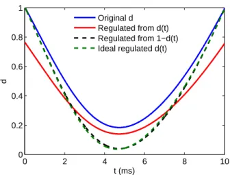
The question is how to change the duty cycle values. It is not enough to change a single duty cycle value, but a full set of values stored in a memory. One possibility is to multiply each value of the memory by the output of the loop, which regulates the mean output voltage. However, the result of this regulation is a distorted duty cycle. Fig. 2 shows the result of multiplying d by a constant when the input voltage is increased. As it can be seen, modifying the duty cycle, it does not start and finish with value 1, which is desired for power factor correction.
0 2 4 6 8 10 0 0.2 0.4 0.6 0.8 1 t (ms) d Original d Regulated from d(t) Regulated from 1−d(t) Ideal regulated d(t)
Fig. 2. Regulation of d and 1 − d parameters
Regulator + - Regulator + + 1-d1 d2 Voutaverage Voutripple
Voutaverage ref
Voutripple ref
d* Regulator + + 1-da Voutaverage
Voutaverage ref
d* 1-d1 + -dc + + d1* db* db*dc* Regulator Voutripple
Voutripple ref
db*dc* * Regulator
1-d Voutaverage
Voutaverage ref
1-d* + -1 da* + -1-da* + -1-d1* 1 1 1-d1* d2** d1* + -+ -+ -+ -+ -1 d*
Regulator vout average
PID error 1 δ k=1+δ + + +
Regulator vout average
PID 1 δ k=1+δ 1 1/k≈ =1-δ + + + -error k k 1/k d2* k dc* ≈ 1/k ≈ 1/k ≈ 1/k ≈
Fig. 3. Control system using d as unique parameter
Therefore, the duty cycle waveform is very different from the ideal, and this affects the input current waveform shape — hence, the power factor.
The proposed solution is to store in memory (1 − d) for each switching period, so this value can be multiplied while keeping the initial and final shapes and, therefore, not being distorted. As it can be seen in Fig. 2, the regulation using (1 − d) is similar to the ideal one.
Figure 3 shows the block diagram of the loop using this technique. As it can be seen, the regulator output, k, is multiplied by the stored complementary duty cycle (1 − d), obtaining the regulated duty cycle (1−d)∗, which is converted into d∗. The regulator is shown with more detail in Fig. 4. There is a PID and its output, δ, is added to ’1’, so the final regulation is 1 + δ. Ideally, in nominal conditions δ is equal to 0, so the output k is 1. However, it is increased or decreased to control the output voltage when necessary, but k remains around 1 under changes in the working conditions.
This method uses (3) under nominal conditions. Changes in the load would not be well detected by this loop, because load changes do not produce significant changes on the average output voltage when the efficiency is high. Therefore, lower power factor will be achieved for other loads. This limitation is overcomed with the following methods.
B. Dividing the duty cycle into two parameters
The previous method cannot compensate for changes in the load of the converter. Further analysis of the duty cycle is shown in this method to overcome this limitation. The d values of (3) can be divided into d1and d2 as follows:
Regulator + - Regulator + + 1-d1 d2 Voutaverage Voutripple
Voutaverage ref
Voutripple ref
d' Regulator + + 1-da Voutaverage
Voutaverage ref
d' 1-d1 + -dc + + d1' db' db'dc Regulator Voutripple
Voutripple ref
dbdc' Regulator
1-d Voutaverage
Voutaverage ref
1-d' + -1 da' + -1-da' + -1-d1' 1 1 1-d1' d2' d1' + -+ -+ -+ -+ -1 d'
Regulator vout average
PID error 1 δ k=1+δ + + +
Regulator vout average
PID 1 δ k=1+δ 1 1/k≈1-δ + + + + + -error
Fig. 4. Regulator used to control d with the voutaverage loop
d1(k) = vout(k) − vg(k) vout(k) d2(k) = L TSw ·(iL(k + 1) − iL(k)) vout(k) d(k) = d1(k) + d2(k) (8)
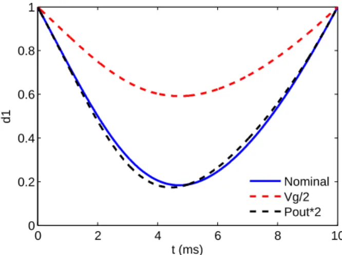
The parameters are shown in Fig. 5 and 6 respectively. As it can be seen, d1is the main component of the duty cycle, while
d2 allows to correct the current distortion produced by the
output load. Fig. 5 shows that d1 is heavily influenced by the
input voltage variation and barely by the power. Taking that into account, d1 can be controlled using the average output
voltage. Thus, the ripple component of vout is ignored, not
being able to change d1 in case of load changes. Similarly to
the first method, 1 − d1 is stored in memory instead of d1,
and the same average output voltage regulator can be used. The d2 component depends on the input current. The input
current, as seen in (6), is proportional to the input/output power of the converter for a given input voltage, so any change in the load would affect proportionally to the input current and so to the d2 component. The system cannot measure the power
of the load directly, but it is able to extract the ripple of the output voltage from the ADC for the output voltage already in use. The ripple of the output voltage is proportional to the output power, as seen in (4). Therefore, sensing the ripple of the output voltage, d2 can be regulated.
On the other hand, d2also depends on the input voltage as
Fig. 6 shows. Therefore, the regulator of the average output voltage is also used to control d2.
The control flow for this method is shown in Fig. 7. As the figure shows, there is an average output voltage loop for d1
(similar to the voltage loop in any PFC converter). Moreover, d2not only uses the same average output voltage loop but also
a ripple output voltage loop. The latter behaves like a classic current loop, although it uses the ripple of the output voltage, but in this case the bandwidth is low.
Similarly to the method presented in subsection III-A, the first component, (1−d1) is regulated with k = 1+δ. However,
the additional component d2 is stored directly, with no use of
complementary terms (1 − d2), so the regulator should output 1
k instead of k, because (1 − d1) and d2 have opposite signs.
This division can be avoided taking into account that 1k =1+δ1 is similar to 1k≈ = 1 − δ, because δ is near 0. For example, if the input voltage is 10% lower than expected, δ is equal to −0.1, so 1 k is approximated to 1.111 and 1 k ≈ = 1.100. In this case, an error of 10% in the input voltage (which is normally much lower) produces an error of 1.01% in the regulation of d2. This simplification reduces drastically the hardware
0 2 4 6 8 10 0 0.2 0.4 0.6 0.8 1 t (ms) d1 Nominal Vg/2 Pout*2
Fig. 5. Representation of d1within the utility semi period.
0 2 4 6 8 10 −0.015 −0.01 −0.005 0 0.005 0.01 0.015 0.02 t (ms) d2 Nominal Vg/2 Pout*2
Fig. 6. Representation of d2within the utility semi period.
resources in use, because a division is much more expensive in terms of area and processing time than an adder, while the resulting error is acceptable. Fig. 8 shows the regulator with two outputs, k to regulate 1 − d1, and 1k
≈
to regulate d2.
This division of parameters into d1 and d2 was also
pre-sented by other authors in [14], [15]. However, in [14], a predictive algorithm and input voltage measuring were im-plemented, instead of using pre-calculated values and adding closed loops measuring only the output voltage. In [15], the input current is also measured. In contrast, the proposed paper avoids measuring this parameter for cost reduction.
C. Dividing the duty cycle into three parameters
The previous d1 parameter, as seen in (8), depends on the
input voltage, but also on the load through the ripple of the output voltage, so it is not symmetric, see Fig. 5. Therefore, further regulation of d1 should be done in order to improve
the power factor if the load is not the same as expected. To achieve further improvements in the duty cycle adjustment, it is proposed to split d1 into two parameters:
Regulator + - Regulator + + 1-d1 d2 Voutaverage Voutripple
Voutaverage ref
Voutripple ref
d* Regulator + + 1-da Voutaverage
Voutaverage ref
d* 1-d1 + -dc + + d1* db* db*dc* Regulator Voutripple
Voutripple ref
db*dc* *
Regulator 1-d
Voutaverage
Voutaverage ref
1-d* + -1 da* + -1-da* + -1-d1* 1 1 1-d1* d2** d1* + -+ -+ -+ -+ -1 d* Regulator vout average
PID error 1 δ k=1+δ + + +
Regulator vout average
PID 1 δ k=1+δ 1 1/k≈ =1-δ + + + -error k k 1/k d2* k dc* ≈ 1/k ≈ 1/k ≈ 1/k ≈
Fig. 7. Control system using d1, d2
Regulator + - Regulator + + 1-d1 d2 Voutaverage Voutripple
Voutaverage ref
Voutripple ref
d* Regulator + + 1-da Voutaverage
Voutaverage ref
d* 1-d1 + -dc + + d1* db* db*dc* Regulator Voutripple
Voutripple ref
db*dc* *
Regulator 1-d
Voutaverage
Voutaverage ref
1-d* + -1 da* + -1-da* + -1-d1* 1 1 1-d1* d2** d1* + -+ -+ -+ -+ -1 d* Regulator vout average
PID error 1 δ k=1+δ + + +
Regulator vout average
PID 1 δ k=1+δ 1 1/k≈ =1-δ + + + -error k k 1/k d2* k dc* ≈ 1/k ≈ 1/k ≈ 1/k ≈
Fig. 8. Regulator used to control d1 and d2with the vout average loop
0 2 4 6 8 10 0 0.2 0.4 0.6 0.8 1 t (ms) da Nominal conditions Vg/2
Fig. 9. Representation of dawithin the utility semi period.
d1(k) = vout(k) − vg(k) vout(k) da(k) = Vout− vg(k) Vout db(k) = d1(k) − da(k) (9)
The waveforms of da and db sequences are shown in Fig.
9 and 10 respectively. The parameter da defines the relation
between the input and output average voltages. Hence, dadoes
not depend on the load, so it is symmetric. However, dbis the
result of subtracting d1 from da, and it depends on the input
voltage but also on the load.
Besides, the dc component is equal to d2:
0 2 4 6 8 10 −0.08 −0.06 −0.04 −0.02 0 0.02 0.04 0.06 t (ms) db Nominal Vg/2 Pout*2
Fig. 10. Representation of dbwithin the utility semi period.
Regulator + - Regulator + + 1-d1 d2 Voutaverage Voutripple
Voutaverage ref
Voutripple ref
d* Regulator + + 1-da Voutaverage
Voutaverage ref
d* 1-d1 + -dc + + d1* db* db*dc* Regulator Voutripple
Voutripple ref
db*dc** Regulator
1-d Voutaverage
Voutaverage ref
1-d* + -1 da* + -1-da* + -1-d1* 1 1 1-d1* d2** d1* + -+ -+ -+ -+ -1 d*
Regulator vout average
PID error 1 δ k=1+δ + + +
Regulator vout average
PID 1 δ k=1+δ 1 1/k≈ =1-δ + + + -error k k 1/k d2* k dc* ≈ 1/k ≈ 1/k ≈ 1/k ≈
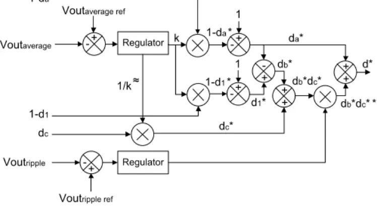
Fig. 11. Control system using da, dband dc
dc(k) = d2(k) = L Tsw · (iL(k + 1) − iL(k)) vout(k) (10) Finally, the duty cycle d is calculated adding the compo-nents da, db and dc:
d(k) = da(k) + db(k) + dc(k) (11)
The values of daand d1should be calculated in order to get
db. In order to respond to input voltage changes, da and d1
have to be controlled with the average output voltage regulator. Besides, dbshould be regulated with the ripple output voltage
controller in order to regulate the load-dependent component. Lastly, dc is equal to d2, so it is controlled using both loops.
The schematic of the proposed regulator is shown in Fig. 11. As it can be seen, the average output voltage regulator is used three times to control (1 − da), (1 − d1) and dc. On the other
hand, the ripple voltage loop is used once to get (d∗b+ d∗c)∗, that is, (d∗b + d∗c) after being regulated by the average output voltage loop.
D. Resolution analysis and quantization
The resolution of the ADC and its quantification effects are critical when using digitally controlled power converters. The
Fig. 12. Model of the average voltage loop
resolution of the ADC and the controller must be analyzed in order to avoid limit cycling in the output voltage loop, which is undesirable. For dc-dc converters, this topic has been deeply studied [16], [17]. In that case, limit cycling is studied taking into account the resolution of the ADC and the PWM signal of the switch. The analysis of resolution and quantification errors is different for PFC converters [18].
An analysis for a classic PFC converter is performed in [18], and similar analysis is done in this work. In a classic PFC converter, the voltage loop outputs the power command signal, which is used in the current loop. Besides, [18] assumes that the current loop is ideal, so it does not alter the average output voltage. However, in this proposal there are not two loops in series. The duty cycle is previously calculated and the system only modifies the pre-calculated values with two loops. Indeed, in the last system, which has the best results as it will be seen, the duty cycle is divided into three parameters: da, db, dc.
The parameters db and dc (also called d2) do not affect
the average output voltage, as it can be inferred analyzing Figs. 10 and 6 respectively, because their mean value over an utility semi-period is zero. Thus, the parameter da is the
only parameter which does alter the average output voltage (Figure 9). Therefore, in this proposal, limit cycling is studied taking into account the resolution of the actuation over da
compared to the resolution of the output voltage ADC. Based on the analysis detailed in [18], there are two mechanisms that can result in low-frequency limit cycling. One is asynchronous sampling of the output voltage with respect to the utility semi-period. However, the proposed PFC technique implies synchronous sampling, as the mean value of the output voltage during a utility semi-period is used for the da loop,
and it is applied when zero crossing is detected. The second mechanism is quantization of the power command. In our case, it is the quantization of k, the parameter that changes the da
component of the duty cycle, as explained in the previous subsections.
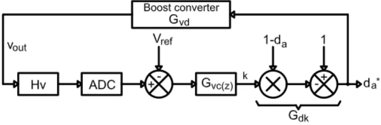
Two conditions must be satisfied to avoid limit cycling due to quantization of the power command: static condition and integral gain for transients. Fig. 12 shows a model of the proposed system with respect to the power command k. In that figure, Hv is the gain of the conditioning circuit of the
output voltage, usually a voltage divider. ADC is the analog to digital converter, and Gvc(z) is the controller that takes into account the mean value of the output voltage, which in our case generates k, that is later translated into a change in the duty cycle component da. The static condition to avoid
limit cycling is that the minimum output voltage step due to
a change in the controller is smaller than a step in the ADC, so the zero error bin can always be reached. This is reflected in:
Gvk0· Hv· qk < qADC (12)
where Gvk0is the low-frequency small signal gain from the
power command k to the output voltage, qk is the resolution
of the regulator, i.e. the LSB of the regulator, and qADC
is the resolution of the ADC, i.e. the LSB of the ADC. If equation (12) is satisfied, there will always be at least a value of the power command inside the zero error bin of the ADC. Gvk0 can be split into:
Gvk0= Gvd0· Gdk0 (13)
where Gdk0is the low-frequency small signal gain from the
power command k to the duty cycle da, and Gvd0is the
low-frequency small signal gain from the duty cycle to the output voltage. In the proposed system, k is multiplied by (1−da) and then subtracted from 1, so Gdk0 is equal to (1− < da >T u),
where < da >T uis the mean value of da over a utility
semi-period. On the other hand, Gvd0 is the low-frequency small
signal gain of the boost converter from the duty cycle to the output voltage, which is equal to:
Gvd0=
< vg>T u
1− < da>T u2
(14) The values of Gvd0and Gdk0depend on the working point
of the converter, so they are calculated for nominal conditions. Finally, the static no limit cycling condition (12) is translated into:
Gvd0· (1 − < da>T u) · Hv· qk< qADC (15)
In our case, (15) is satisfied when:
Gvd0· (1 − < da >T u) · Hv· qk < qADC 695.6522 · (1 − 0.425) · 5 500 · qk < 5 · 1 210 qk< 0.0012 (16)
The regulator used in the experimental results uses 14 frac-tional bits, so qk = 2−14 = 0.00006 << 0.0012. Therefore,
the static no limit cycling condition is satisfied. A comment about the resolution of the duty cycle is also necessary, as the power command k influences the duty cycle which is fed into the power converter. The static no limit cycling condition necessary for dc-dc converters is also necessary in the proposed PFC technique, because the power command k changes the mean duty cycle during an utility semi-period. However, the mean duty cycle is obtained with all the duty cycle values of an utility semi-period, so there is an intrinsic dither technique [16] when obtaining the mean duty cycle. As a consequence, the static no limit cycling condition is as shown in (17), but will be easily met thanks to the intrinsic
dither technique of calculating the mean duty cycle over an entire utility semi-period.
Gvd0· Hv· qDP W M #swcyc < qADC 695.6522 · 5 500 · qDP W M 1000 < 5 210 qk < 0.7 (17)
where qDP W Mis the resolution of the DPWM and #swcyc
is the number of switching cycles during an utility semi-period, which is 1000 in our case. The controller used in the experimental results uses 15 bits for the DPWM (see section IV), including 5 bits for dither as explained in [16]. Therefore, qDP W M = 2−15 = 0.00003 << 0.7, so the static
no limit cycling condition due to duty cycle resolution is also met.
The previous conditions check if there is an output of the regulator which is inside the zero error bin of the A/D converter (static condition). However, limit cycling can also appear after a transient if the integral gain is so high that the zero error bin can be crossed in a single regulator cycle. The dynamic no limit cycling condition is:
Gvk0· Hv· Ki< 1 (18)
where Ki is the integral gain of the regulator. In our case,
this gain is equal to 2−11, so the dynamic condition is also satisfied: Gvd0· (1− < da>T u) · Hv· Ki< 1 695.6522 · (1 − 0.425) · 5 500 · 2 −11< 1 0.002 << 1 (19) As a conclusion, in order to avoid limit cycling with the proposed PFC technique, the same condition as in dc-dc converters must be reached (resolution in the DPWM finer than the resolution of the ADC converter), but using the effective resolution of the mean DPWM over an utility semi-period. Furthermore, the power command k must have enough resolution, and the integral gain of the regulator that generates k can not be very high. The resolution of the DPWM is a deeply studied topic, while a high resolution of the power command k is easy to obtain, as it is an internal variable of the controller that can be generated with arbitrary resolution. However, using the same resolution as in the DPWM is enough, as the power command is finally used to change the mean duty cycle.
IV. EXPERIMENTAL RESULTS
In this section, all the methods described before are tested and compared by means of a prototype of the converter and regulators. The configuration of the prototype is presented in Section IV-A and experimental results are shown in Section IV-B.
A. Implementation
The controller has been implemented using an FPGA Xilinx XC3S1000-4FT256. The clock of the system is 50 M Hz and it is doubled with a DCM (Digital Clock Manager), so the final clock frequency is 100 M Hz. The switching frequency is 100 kHz, getting a PWM with duty cycle values between 0 of 999. Finally, the ac mains frequency is 50 Hz and 100 Hz after the rectification, so there are 1 000 switching cycles inside an ac mains semi-period.
The values of the duty cycles are accurately pre-calculated offline in a computer (with any tool such as Matlab, any high-level programming language or even with non-synthesizable VHDL). The calculated duty cycles are stored in the FPGA so the system can use them. Indeed, depending on the control method, the final duty cycles or the divided parameters of those duty cycles are stored in memory. For instance, using the first method, the whole duty cycle is stored with format (1 − d), using the second method, parameters (1 − d1) and
d2 are stored, and using third method, parameters (1 − da),
(1 − d1) and dc are written. The block RAMs of the FPGA
are used to store these values. Every parameter is written in 16 bits, using 11 bits to store a value between 0 and 999 in two’s complement, and 5 bits to store fractional values of the duty cycle components. These fractional values are used to implement a dither technique [16] which increases the resolution of the PWM. Therefore, each parameter stored in memory uses 16 000 bits, less than one block RAM of the FPGA (this FPGA can be configured with 24 modules of 16 kb).
Simple PID controllers for the average output voltage loop and load loop, by means of the ripple output voltage, have been implemented using fixed-point notation. As stated before, the average output voltage loop is similar to the voltage loop of a classic PFC converter, so it is a low frequency loop. On the other hand, the ripple output voltage loop behaves like a current loop, but it differs from classic current loops because it also has low frequency, as its input is the ripple of the output voltage through an input voltage cycle.
The ADC used in the experimental results has 10 bits of resolution and its sampling frequency is 100 kHz. It is an ad-hoc Σ∆ ADC, using a voltage comparator and an RC filter as only analog components, while the digital logic is implemented inside the FPGA (see [8] for details). This ADC has been chosen to decrease the cost, but any commercial ADC of 10 bits and around 10 kSP S (kilosamples per second) can be used. The sampling frequency must be enough to measure the output voltage many times inside an utility period, so the mean and ripple value can be calculated accurately. However, 10 kSP S are enough, because with this sampling, 100 measures are taken inside the utility period.
The output voltage ADC takes samples during an ac mains half-period and an average of those values is calculated to feed the first loop. The same ADC samples are read in order to get the maximum and minimum value inside a half-period and, hence, the output voltage ripple. Finally, the duty cycles stored in the memories have to be synchronized with the ac mains. This is done using a voltage comparator, which compares
TABLE I CONVERTERPARAMETERS Parameter Value FSW 100 kHz L 5 mH C 68 µF P 300 W Vg 230 V Vout 400 V TABLE II
FPGA (XILINXXC3S1000)RESOURCES USED BY ALL METHODS
Method 4 input FFs Mult BRAMs
LUTs 18x18 (16 kB) Method 1: 165 91 2 1 d (1.07%) (0.59%) (8.33%) (4.17%) Method 2: 245 109 5 2 d1 and d2 (1.60%) (0.71%) (20.83%) (8.33%) Method 3: 309 109 6 3 da, dband dc (2.01%) (0.71%) (25%) (12.5%) Sync, PWM, 828 457 2 0
ADC controller, etc (5.39%) (2.98%) (8.33%) (0%)
the input voltage (driven through a resistor divider) and a voltage reference. When the input voltage is below 10 V , the comparator sets a ’1’ in its output and otherwise it drives a ’0’. A simple digital debounce filter has been implemented in the FPGA to erase the noise of the output of the comparator, and it generates the synchronization signal which will be used by the memories and controllers. Therefore, the system uses just one comparator for ac mains synchronization, and one ADC for the output voltage.
The parameters of the converter are shown in Table I. These parameters are used in all the experiments unless otherwise noted.
Table II shows the FPGA implementation results of the three methods. As it can be seen, most of the LUTs and flip flops are used in the synchronization with ac mains, PWM calculation, ADC controlling, etc. None of the controlling methods use many resources, so the decision on which method should be implemented should not be made based on the necessary hardware resources.
B. Results
All the proposed methods have been tested and the results are shown in this subsection for validation of the proposals and comparison. As it is presented next, testing includes load changes and harmonics normative compliance.
All current THD values as well as power factors and harmonics have been measured using a Voltech PM1000+ power analyzer.
The first experiment has been accomplished to test all the methods with different loads. In this way, the second loop, the ripple output voltage loop, is checked. The average voltage loop is running anyway, because it is always necessary to control the output voltage in its nominal condition. In all cases, the duty cycles were pre-calculated for P = 300 W , so Fig. 13 shows the control loops performance in steady state. As it can be seen in Fig. 13, the third method (da, db, dc) achieves
0.65 0.70 0.75 0.80 0.85 0.90 0.95 1.00 33 72 147 221 300 D D1, D2 Da, Db, Dc P (W) Powe r factor
Fig. 13. Power factor of all methods with different loads. Duty cycles pre-calculated for V g = 230 V , P = 300 W and Vout= 400 V
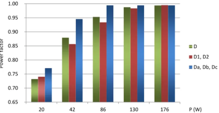
0.65 0.70 0.75 0.80 0.85 0.90 0.95 1.00 20 42 86 130 176 D D1, D2 Da, Db, Dc P (W) Powe r factor
Fig. 14. Power factor of all methods with different loads. Duty cycles pre-calculated for V g = 120 V , P = 176 W and Vout= 300 V
much better results when the load has not its nominal value. It may be thought that the second method (d1, d2) is better than
the first method (d), because it regulates d2 with the ripple of
the output voltage while the first method does not. However, it does not take into account the ripple in the d1component, and
the regulation of d2 without taking into account the ripple in
d1is counterproductive. This can be explained seeing Fig. 10,
which shows db, i.e. the distortion of d1. As it can be seen
by comparing d2 and db in Figs. 6 and 10 respectively, db
is bigger than d2, and that is why the d1, d2 method obtains
similar or worse results than using only d.
Tests have been also carried out with Vg = 120 V ,
Vout= 300 V and P = 176 W , which are shown in Fig. 14.
All the methods achieve better results with 120 V . With this configuration, the third method also gets much better results, and the second method (d1, d2) again gets the worst results.
The waveforms of the input current, and input and output voltages are shown in Fig. 15, in nominal conditions (Table I).
All the methods have been tested in order to know if they pass the standard for harmonics regulation EN 61000-3-2. All classes (A, B, C and D) have been checked, and all the methods pass the tests in nominal conditions. Table III shows the results of the third method (da, db, dc) passing the class C
standard, which is the most restrictive. As it can be seen, all the harmonics which have been checked are much lower than the standard limits.
The system only uses one ADC, and all the regulation is accomplished using the data acquired with this ADC.
Fig. 15. Waveforms of method da, dband dc. Output voltage (top), input current (middle), input voltage (bottom)
TABLE III
IEC 61000-3-2 CLASSCTEST
Harmonic Measured value Maximum allowed Pass
1st 1.390 Yes
2nd 0.0035 0.028 Yes
3rd 0.135 0.414 Yes
5th 0.045 0.139 Yes
7th 0.020 0.097 Yes
Therefore, it is important to know how sensible the system is to quantization errors of the ADC. Another experiment has been done in order to check this sensibility. The value given by the ADC has been increased and decreased artificially in order to simulate the quantization error of the ADC. The error by means of THDi o PF is small when the value the ADC is increased o decreased by 1, so it is hard to quantify the error. Therefore, the ADC value has been modified by 16, and then the result is divided by 16 in order to obtain the variation per bit. An error of 16 LSB in the average output current deteriorates the current THD by an additional 0.9879%, so each LSB corresponds to 0.0617%. If the same 16 LSB error is applied to the ripple of the output voltage, then the current THD deteriorates by an additional 14.954%, so each LSB corresponds to 0.9346%. The system is more sensitive to changes in the ripple value than in the average value. It is normal, because the same change is more representative with the ripple value (about 30 V ), than with the average value (400 V ). Because of this circumstance, the ADC resolution becomes critical when the output voltage ripple is very low.
As equation (3) shows, the duty cycle depends on the inductance. Higher values of the inductance make easier to achieve high PFC. This is because the higher the inductance, the higher the second component of equation (3), and it will be easier to control this component. This was explained with further details in [19]. Once a value is fixed, which is used to pre-calculate the duty cycles, the real inductance will be slightly different than the expected value. An experiment has been accomplished, and an inductor with its inductance 10% lower than expected has been used. Using the same working conditions (see Table I) the experimental results for current THD are 6.30% for nominal inductance and 6.50% for a 10% lower inductance. As it can be seen, the error of the inductance
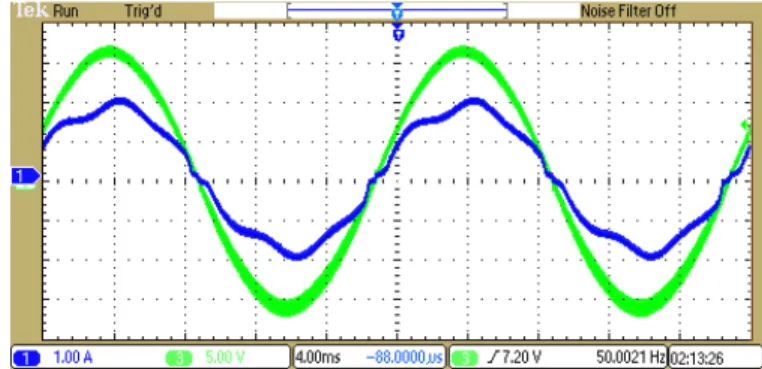
Fig. 16. Input current when the input voltage 3rd and 5thharmonics are 1% distorted. 120 V rms input voltage (green), input current (blue).
TABLE IV
POWERFACTOR AND CURRENTTHDWHEN THE INPUT VOLTAGE3rdAND 5thHARMONICS ARE DISTORTED.
3rd& 5th Vg= 120 V , 176 W Vg= 230 V , 300 W
harm. distor. PF THDi PF THDi
0% 0.995 9.56% 0.993 9.30%
1% 0.995 8.00% 0.972 24.00%
2% 0.979 20.40% 0.901 48.00%
3% 0.951 33.70% 0.810 73.00%
estimation is not critical. The reason is that it only influences on the dc component, which is notably smaller than d1.
The proposed system only measures the output voltage, not measuring neither the input current nor the input voltage. In real applications, the input voltage frequently has harmonic content, specially in the third and fifth harmonics. Due to the lack of these measures, the system cannot detect this distortion, so power factor is heavily influenced by this harmonic content. Table IV shows the results of system when the input voltage is distorted. As it can be seen, the system is more affected in the case of higher input voltage. The IEC 61000-3-2 current limits are met for all the classes when the input voltage is 120 V rms and it has 3rd and 5th harmonic components of 1%. When these harmonic components are 2% and 3%, the classes A, B and D are passed, but the class C is not. With an input voltage of 230 V rms, the current limits of the classes A, B and D are met with harmonic components of 1% and 2%, and the classes A and B also are passed with 3% distortion, but class C is not passed. Figure 16 shows the input current and input voltage when the input voltage (120 V rms) has harmonic components of 1%.
V. CONCLUSIONS
This paper presents an input current sensorless method for PFC converters. Furthermore, the input voltage is not measured through an ADC but only a voltage comparator is used for zero-crossing detection. Pre-calculating offline the duty cycles of the converter for nominal conditions, high power factor is reached. In order to make the converter more robust, two control loops have been implemented. The first loop, which acts like a classic voltage loop, measures the average output voltage. The second one replaces the classic current loop, but working at low frequency and only measuring the ripple of the output voltage, which is proportional to the
load of the converter. An exhaustive analysis of the duty cycle calculus is presented and the duty cycles have been divided into sub-parameters to control them separately with both loops. Results show that up to 99.5% power factor is reached for nominal conditions, and it is also high in case of changes in the output load. As the system does not measure the input voltage, its harmonic content deteriorates the power factor.
All the complex calculus of duty cycles are accomplished offline and once in an external device. The FPGA reads the duty cycle from a memory and implements two simple PID regulators for both loops. In this way, the system can be implemented in a low-cost device.
REFERENCES
[1] P. Midya, P. Krein, and M. Greuel, “Sensorless current mode control-an observer-based technique for dc-dc converters,” Power Electronics, IEEE Transactions on, vol. 16, no. 4, pp. 522–526, Jul. 2001. [2] Y. Qiu, X. Chen, and H. Liu, “Digital average current-mode control
using current estimation and capacitor charge balance principle for dc-dc converters operating in dc-dcm,” Power Electronics, IEEE Transactions on, vol. 25, no. 6, pp. 1537–1545, Jun. 2010.
[3] M. Rodriguez, V. Lopez, F. Azcondo, J. Sebastian, and D. Maksimovic, “Average inductor current sensor for digitally controlled switched-mode power supplies,” Power Electronics, IEEE Transactions on, vol. 27, no. 8, pp. 3795–3806, Aug. 2012.
[4] Z. Lukic, Z. Zhao, S. Ahsanuzzaman, and A. Prodic, “Self-tuning digital current estimator for low-power switching converters,” in Applied Power Electronics Conference and Exposition, 2008. APEC 2008. Twenty-Third Annual IEEE, Feb. 2008, pp. 529–534.
[5] K. Hwu, H. Chen, and Y. Yau, “Fully digitalized implementation of PFC rectifier in CCM without ADC,” Power Electronics, IEEE Transactions on, vol. 27, no. 9, pp. 4021–4029, Sep. 2012.
[6] B. Mather and D. Maksimovic, “A simple digital power-factor correction rectifier controller,” Power Electronics, IEEE Transactions on, vol. 26, no. 1, pp. 9–19, Jan. 2011.
[7] Y.-S. Roh, Y.-J. Moon, J.-C. Gong, and C. Yoo, “Active power factor correction (PFC) circuit with resistor-free zero-current detection,” Power Electronics, IEEE Transactions on, vol. 26, no. 2, pp. 630–637, Feb. 2011.
[8] F. Azcondo, A. de Castro, V. Lopez, and O. Garcia, “Power factor correction without current sensor based on digital current rebuilding,” Power Electronics, IEEE Transactions on, vol. 25, no. 6, pp. 1527–1536, Jun. 2010.
[9] V. Lopez, F. Azcondo, F. Diaz, and A. de Castro, “Autotuning digital controller for current sensorless power factor corrector stage in continu-ous conduction mode,” in Control and Modeling for Power Electronics (COMPEL), 2010 IEEE 12th Workshop on, Jun. 2010, pp. 1–8. [10] H.-C. Chen, “Single-loop current sensorless control for single-phase
boost-type SMR,” Power Electronics, IEEE Transactions on, vol. 24, no. 1, pp. 163–171, Jan. 2009.
[11] H.-C. Chen, C.-C. Lin, and J.-Y. Liao, “Modified single-loop current sensorless control for single-phase boost-type SMR with distorted input voltage,” Power Electronics, IEEE Transactions on, vol. 26, no. 5, pp. 1322–1328, May 2011.
[12] I. Merfert, “Analysis and application of a new control method for continuous-mode boost converters in power factor correction circuits,” in Power Electronics Specialists Conference, 1997. PESC ’97 Record., 28th Annual IEEE, vol. 1, Jun. 1997, pp. 96–102 vol.1.
[13] I. W. Merfert, “Stored-duty-ratio control for power factor correction,” in Applied Power Electronics Conference and Exposition, 1999. APEC ’99. Fourteenth Annual, vol. 2, Mar. 1999, pp. 1123–1129 vol.2. [14] W. Zhang, G. Feng, Y.-F. Liu, and B. Wu, “A digital power factor
cor-rection (PFC) control strategy optimized for DSP,” Power Electronics, IEEE Transactions on, vol. 19, no. 6, pp. 1474–1485, Nov. 2004. [15] W. Zhang, Y.-F. Liu, and B. Wu, “A new duty cycle control strategy for
power factor correction and FPGA implementation,” Power Electronics, IEEE Transactions on, vol. 21, no. 6, pp. 1745–1753, Nov. 2006. [16] A. Peterchev and S. Sanders, “Quantization resolution and limit cycling
in digitally controlled PWM converters,” Power Electronics, IEEE Transactions on, vol. 18, no. 1, pp. 301–308, Jan. 2003.
[17] H. Peng, A. Prodic, E. Alarcon, and D. Maksimovic, “Modeling of quantization effects in digitally controlled dc-dc converters,” Power Electronics, IEEE Transactions on, vol. 22, no. 1, pp. 208–215, Jan. 2007.
[18] B. Mather and D. Maksimovic, “Quantization effects and limit cycling in digitally controlled single-phase PFC rectifiers,” in Power Electronics Specialists Conference, 2008. PESC 2008. IEEE, Jun. 2008, pp. 1297– 1303.
[19] A. Garcia, A. de Castro, O. Garcia, and F. Azcondo, “Pre-calculated duty cycle control implemented in FPGA for power factor correction,” in Industrial Electronics, 2009. IECON ’09. 35th Annual Conference of IEEE, Nov. 2009, pp. 2955–2960.
Alberto Sanchez was born in Madrid, Spain, in 1986. He received the M.Sc. degree in computer science and telecommunication engineering from the Universidad Autonoma de Madrid, Spain, in 2010, where he is currently working toward the Ph.D. degree in the Technology for Electronics and Communications Department. His research interests include digital control of switching mode power supplies and wireles sensor networks with mobile nodes.
Angel de Castro (M’08) was born in Madrid, Spain, in 1975. He received the M.Sc. and the Ph.D. degrees in electrical engineering from the Universidad Politecnica de Madrid, Madrid, Spain, in 1999 and 2004, respectively. He has been an Associate Professor in the Universidad Autonoma de Madrid since 2010, and as Assistant Professor from 2006 to 2010. Previosly, he was an Assistant Professor in the Universidad Politecnica de Madrid since 2003. His research interests include digital control of switching mode power supplies, field programmable gate arrays and mobile nodes in wireless sensor networks.
Victor Manuel L´opez (S’10) was born in Tor-relavega, Cantabria, Spain, in 1985. He received the Electronics and Control Engineering degree from the University of Cantabria, Santander, Spain, in 2009, where since then he has been working toward the Ph.D. degree in the Department of Electronics Technology, Systems and Automation Engineering (TEISA). Since June to September 2012, he was Visiting Schoolar in the Colorado Power Electronics Center (CoPEC), University of Colorado at Boulder, and since September to December 2012 in the Utah State University Power Laboratory, at Logan, Utah. Both periods with the Prof. Regan Zane as advisor. His research interests include design, modeling, and digital control of topologies for AC-DC converters and for resonant inverters. Mr. Lopez received the IEEE/IEL Electronic Library Award in 2009.
Francisco J. Azcondo (S’90M’92SM’00) received the electrical engineering degree from the Universi-dad Politcnica de Madrid, Madrid, Spain, in 1989, and the Ph.D. from the University of Cantabria, Spain, in 1993. From 1995 to 2012 he was Asso-ciate Professor in the TEISA Dept. at ETS II y T, University of Cantabria. Since 2012 he is Professor in the Same Dept. From February to August 2004 and 2010, he was a Special Member of the ECEE Department, University of Colorado, Boulder, and in the summer of 2006, a Visiting Researcher in the ECE Department, University of Toronto, ON, Canada. He was chair of the IEEE IES PELS Spanish Joint Chapter from Sept. 2008 to June 2011. His research interests include modeling and control of switch-mode power converters and resonant converters, digital control capabilities for SMPS, current sensorless control for power factor correction stages and applications such as outdoor lighting, electrical discharge machining, and arc welding.
Javier Garrido (M’97) was born in Madrid, Spain, in 1954. He received the B.Sc. degree in 1974, the M.Sc. degree in 1976 and the Ph.D. degree in 1984 in Physics from the Universidad Autonoma de Madrid, UAM (Spain). Since 1992 he has been participated, in the implementation of the Computer Science (1992) and Telecommunication (2002) en-gineering studies at the Polytechnic School (EPS-UAM), and he got his current position as Full Professor at 2010. From his incorporation to the EPS, he has extended his research interests to topics related with HW/SW applications on embedded systems (microcontrollers, microprocessors, FPGAs and SOC devices) as platforms for wireless sensor nets (WSN) or robotic sensor agents (RSA). In 2003 he co-founded the HCTLab group, (Human Computer Technology Laboratory) and now he is its director. Dr. Garrido has been participated in several R&D projects and has published more than 40 articles in peer-review journals and 60 papers in archived conference proceedings.