TítuloNew Toroidal Beam Antennas for WLAN Communications
24
0
0
Texto completo
(2) such required characteristics. Much of the effort has been devoted towards antennas based on patches, because of their ease manufacturing and low cost, but at the price of obtaining solutions with narrow impedance bandwidths, a characteristic that constitutes the main drawback of that kind of radiating devices [2]. As cited by Mayhew-Ridgers [3], and according to Pozar [4], bandwidth enhancement is essentially acquired by means of three approaches: impedance matching, multiple resonances, and use of lossy materials. Multiple resonances often imply complicated devices, and the use of lossy materials is not always justified, due to the resulting reduction of the radiation efficiency of the antenna. During recent years some electromagnetically coupled (EMC) stripline-fed patch configurations have shown very good results, improving the bandwidth scattering matrix entry S11 up to 30% [3-6]. The success of this technique lies in the insertion of a conductor that behaves capacitively, thus compensating the inductive impedance of the coaxial pin used for feeding configurations with thick dielectrics [3]. Unfortunately, the proposed configurations exhibit relatively bad -symmetry [6-7] of the radiation pattern. It is reasonable that several radiating elements arranged in a circular array can generate a toroidal beam, provided that the pattern of every element is appropriately selected. Such arrangement suggests the possibility of extending the techniques, making use of a singleelement with rotational symmetry, with a geometrical configuration of the type of the previously mentioned array. These are the outlines of the novel configurations explored in this paper. In the numerical simulations, the thicknesses of the metal parts of the antennas are taken equal to 0.002 mm in all the simulations, a standard value used in the design of this kind of geometries.. 2. A CIRCULAR ARRAY OF CIRCULAR PATCHES As discussed above, we explore the possibility that several L-probe fed patch elements of the same kind may be arranged along a circular ring so as to radiate a prescribed toroidal beam, provided that every element radiates a sum pattern with its maximum shifted from the normal. If the array is built so that the electromagnetic coupling between neighbouring elements is negligible, then the single-element impedance is not significantly modified. Accordingly, a two-stages procedure must be pursued: first, design of a single element that satisfies the impedance (broad) band requirements; then, design of a circular array composed of above presented elements, placed as close as possible among themselves –to obtain a broad beamwidth–, but separated enough to minimize mutual coupling –to avoid a severe impedance bandwidth reduction. This can be achieved by the use of any Method of Moments (MoM) commercial software tool [8], as outlined in the next sections. 2.1. FIRST STAGE: DESIGN OF A SINGLE L-PROBE FED CIRCULAR PATCH Figure 1 shows the geometry of the element whose design is performed at this stage. It consists of a circular radiating patch of radius RR with a microstrip line (ML) of width wM and Page 2 of 24.
(3) length lM, placed below the patch at a distance hFR; a coaxial probe that feeds the ML; and, finally, an infinite ground planeI located at a distance hGF below the ML, all of them placed on a two-layer rigid dielectric (not shown in the figure for simplicity), with r=1. The ML is placed in a direction parallel to a radius of the patch, and its dimensions and position are to be adjusted so as to produce the best impedance matching, in terms of the relative bandwidth:. f f BW(%) 100 H L (1) fC where fH and fL are the higher and lower frequencies, respectively, within which the amplitude of S11 maintains its valueII below 10 dB, whereas fC is the central frequency, defined as:. fH fL (2) 2 The radius of the patch is chosen to be less than /2, so that it radiates just a main lobe, fC . and is selected to produce the appropriate frequency shift of the bandwidth, since its size controls such a frequency displacement. Impedance matching (and broadening) is also controlled by the distances hGF and hFR. The proper selection of these parameters (RR, hGF and hFR) determines the performance of the radiating patch. 2.2. SECOND STAGE: DESIGN OF THE CIRCULAR ARRAY The second stage design consists in placing several elements, designed at the previous stage, in a circular arrangement, see Figure 2; and then in making additional changes until the desired specifications are accomplished. The rotational symmetry and the width of the main beam are both controlled by the number of elements. This number plays also an important role in the impedance matching, because the elements cannot be placed too close among themselves, under penalty of obtaining an electromagnetic coupling that reduces the S11 bandwidth. The parameter that must be further determined at this stage is the radius of the ground plane RG, whose value is determined by the tolerable back radiation (the bigger the plane, the lower the back lobes, as expected) and by the frequency shift of S11. Above kind of arrangement is very easy to design but, unfortunately, it exhibits a drawback: the number of needed coaxial pins is equal to the number of the array elements. This requires a corresponding feeding network that must be placed below the ground plane, leading to a solution that implies an additional effort from the designer. An alternative to this solution is described in next subSection.. I. This choice allows the reduction of the computing time. Nevertheless, a high accuracy is not of critical importance at. this stage: refinements in calculations are left to the final additional steps of the design, as shown in next Sections. II. In what follows, S11 indicates the amplitude of the scattering parameter, i.e., |S11|. Page 3 of 24.
(4) 2.3. ADDITIONAL THIRD STAGE: CIRCULAR ARRAY WITH A SINGLE FEEDING POINT An alternative design, aimed to the reduction of complexity in the feeding network of the model given in subSection 2.2, can be accomplished by grouping all the MLs and then inserting a common coaxial probe, as shown in Figure 3. In such a case, the presence of coupling fields in the centre of the array, and the change of input impedance of all MLs now grouped in a common conductor, surely requires to change both the initial width and length of every stripline. It must be pointed out that this is a trial solution that not always produces the best results, even when width transitions are inserted between the probe and the MLs obtained at the first stage. 2.4. FURTHER EXTENSION OF THE ABOVE TECHNIQUES: CIRCULAR RING PATCH RADIATOR WITH A CIRCULAR FEEDER As commented under Section 1, the array configurations shown in last subSection intuitively suggest the possibility of building a model in which the circular elements are replaced by a single circular ring with dimensions comparable to those of the array itself (see Fig. 4). This guarantees an excellent rotational symmetry with a simplified model (compared with an array), at the price of a somehow decreased S11 performance, as shown in the corresponding examples (see Section 4). The maximum bandwidth is acquired through the proper impedance matching, by means of the appropriate selection of the vertical distances hGF, hFR, the radius of the circular feeder RF, and the outer and inner radii (RR and RH, respectively) of the radiator (provided that the dielectric layers permittivities are selected to be r1 = r2 = 1, as in the examples presented under previous subSections).. 2.5. CIRCULAR (FILLED) PATCH RADIATOR WITH A CIRCULAR FEEDER A further simplification of the designs described in subSection 2.4 is easily obtained by closing the hole of the radiator (i.e. RH=0), which, after readjusting the rest of the dimensions, leads to an additional reduction of the S11 performance. All models described hitherto are presented with examples in Section 4. In addition, a (free) step-by-step procedure for any of the designs presented here, organized in the form of a practical recipe, can be requested by the interested reader via email to the first author of this paper.. 3. PERFORMANCE PARAMETERS FOR COMPARING DIFFERENT MODELS Since all the antennas modelled with the abovementioned procedures share some common characteristics, they should be compared in terms of meaningful parameters. We make use of the conventional ones, as S11 bandwidth and average value within it, main lobe Page 4 of 24.
(5) beamwidth (in terms of a minimum gain, conveniently established) and maximum gain at central and edge frequencies (fC, fL, and fH). But we also introduce additional quality parameters, as follows. We define the weighted standard deviation of S11 within the bandwidth,, as: 1/ 2. fH 2 1 (3) df S11(f ) S11, AV Exp f fC . f fH fL L In Eq. (3), fH and fL are the higher and lower frequencies defined above, which specify the. attained beamwidth; S11, AV is the average value of S11: S11, AV . 1 fH fL. . fH fL. df S11(f ) ,. (4). and (in frequency units) is a weighting factor that may (or may not) be taken equal to one half of the bandwidth, see the following considerations. The philosophy underlying Eq. (3) is as follows. The assertion that S11 should remain under a prescribed value within the bandwidth is quite obvious. But it is also desirable that its oscillations within the bandwidth remain also limited, because a sensible S11 frequency dependence may degrade the faithful reception of the signal. This obviously leads to the requirement of taking also the S11 mean square deviation [S11(f)S11,AV]2 under control. However, the deviation of S11 from its mean, close to the beamwidth borders, is unavoidable, because it is forced there to reach its maximum value: accordingly, the contribution of this frequency section of S11 to the mean square deviation should be lowered compared to the similar contribution of the central part, where S11 has more freedom to change; and this accounts for the exponential term appearing in Eq. (3). The choice of the factor takes care of the intensity of the weight: the larger , the lower the weight, and vice–versa. We conclude that a measure of the antenna quality performance is provided, among others, by small values of the factor. The parameter , Eq. (3), accounts for the array performance as a load for the feeding network. Additional parameters are needed to judge the performance of the designed model as a radiating system, and these are introduced in what follows. The normalized field intensity, Fx(,), at central X=C, and extreme, X=L, H, frequencies is defined as: FX , E X , . 2. E C 0 , 2. (5). wherein 0 is the nominal direction of maximum radiation for the central frequency beamIII, and |EX(,)|2 is the copolar component of the radiated electric field, which represents the E component in the models designed here, being E the corresponding crosspolar componentIV.. III. We implicitly assume that 0 is independent. If this is not the case (as happens with the models considered in this work), an. average value is taken.. Page 5 of 24.
(6) A quality parameter describing the deviation of the shape of the radiation diagram moving from the central to any of the extreme frequencies is of interest. A convenient measure is the mean square deviation: ½. 1 1 2 FC 2 (6) X 0 d d FX , FC , IC 2 C where C=FCIC is the nominal angular apertureV of the beam for the central frequency around the direction of maximum radiation 0, and defined as the region within which the gain is above 3 dBi. It is evident that the smaller the X, the better the antenna performance within the operating bandwidth. Another quality parameter is the ripple of the radiation diagram, as we move around the coordinate. Defining the average value of the field intensity as a function of : FC,AV . 1 2 d FC , , 2 0. (7). the maximum ripple at central frequency is, then, given byVI:. . . MAX Max 10log10 FC , FC,AV .. (8). As usual, the smaller MAX, the better is the performance of the array within the operating bandwidth. The polarization purity is defined at the operating central frequency, as customarily made, by the ratio. . ARMIN Min 10log10 E,C , . 2. . 2 E,C , , . (9). in order to determine its worst value within the coverage zone. We note that the introduced parameters provide numbers, and not graphs, which is a convenient measure to compare the performance of different constructions of analogous radiating systems. In order to facilitate the reading of the next Sections of the paper, a list containing the definitions of all relevant parameters defined throughout this paper is given in Table 1.. IV. In what follows, E and F refer, unless explicitly specified, to the copolar component of the field and the normalized field intensity,. respectively, see Eq. (5). V. Again, we implicitly assume that C is independent. If this is not the case (as happens in this work), averaged values of IC and. fC must be taken. VI. The similar definition for the extreme frequencies is straightforward and it is not included here for simplicity.. Page 6 of 24.
(7) 4. EXAMPLES OF NUMERICAL DESIGNS In what follows we present several examples, according to the guidelines given above. SubSections 4.1 to 4.5 are ordered accounting to the design procedures described under subSections 2.1 to 2.5.. 4.1. L-PROBE FED CIRCULAR PATCH For a design frequency of 5.24 GHz (=57.21mm) –compatible with one of the WLAN standard frequencies [9]–, and according to the outlines given in Section 4.1 (the diameter of the probe was selected to be equal to 1 mm), a numerical prototype was designed, giving the following geometrical characteristics: RR = 12 mm, lM = RR, wM = 1.5 mm, and hGF = hFR = 3 mm. The S11 of this model remains below –10 dB from fL = 4.96 GHz to fH = 6.29 GHz, leading to an fC = 5.61 GHz and a bandwidth BW = 23.64%. For this paper size limitation, the S11 curve of this design as well as the parameter are not shown here, leaving this information and related discussion to the more relevant cases fully evaluated in the subsequent subSections.. 4.2. CIRCULAR ARRAY WITH SEVERAL FEEDING POINTS With the array element designed in Section 4.1, two arrays have been numerically synthesized. The Model A geometry, composed of 6 elements, is that shown in Fig. 2. This model exhibits geometrical and performances parameters that are listed in Tables 2 and 3, respectively. If the initial geometric parameters of every element, listed in Section 4.1, are maintained, this arrangement reduces of about 2% the S11 bandwidth given by the singleelement. A maximum gain GMAX = 10.46 dBi is obtained at the frequency fH (back radiation always below 0 dBi). A coverage zone of H= FH–IH = 33.48º is obtained in the worst case, with a rotational symmetry guaranteed by a MAX=0.08 dB. In order to make uniform the comparison between all models generated (see next subSections), the parameter has been calculated by assuming for all cases =0.06, which represents (fH–fL)/2 for model F (subSection 4.4). Examination of L and H (both equal to 0.150) shows that the degradation of power pattern of Model A has a symmetrical behaviour. Model B is composed of 4 elements. Compared to Model A, their dimensions are reduced (RG= 45 mm, and RCC = 22 mm). The S11 bandwidth turns out to be similar to that obtained with the 6-elements model (BW=21.16%), but the parameter is somewhat reduced. The S11,AV is, nevertheless, slightly increased. Within the coverage region, the pattern shows a MAX=0.02 dB, which represents a very good result. The power pattern degradations at fH is increased, compared to Model A, as shown by examination of the parameters.. Page 7 of 24.
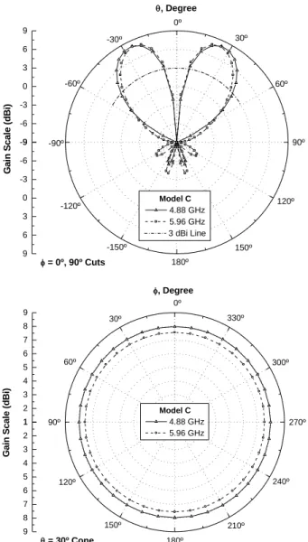
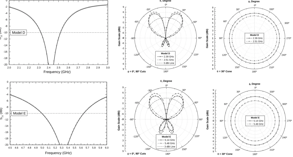
(8) 4.3. CIRCULAR ARRAY WITH ONE FEEDING POINT Model A can be used as starting step to apply the outlines commented in Section 2.3. Good results are obtained with this new arrangement, referred to as model C, and depicted in Figure 3. Its geometrical parameters, together with the characteristics of both the pattern and S11, are listed in Tables 2 and 3. Comparison with Model A reveals that some initial geometric parameters have been slightly changed, due to some adjustments in the final design steps (RR changed from 12 to 13 mm, reduction of ground plane, etc.). In this case, RF represents the distance from the center of the array to the edge of any of the microstrip lines, as established in Table 1. Fig. 5 shows the S11 vs. frequency curve (left), the polar plots of the power pattern at extreme frequencies vs. (right top) and vs. (right bottom); Fig. 6 shows the 3-dimensional power pattern plot generated by this antenna. It can be seen that this is a numerical prototype with good performances: the rotational symmetry is quantified by a MAX=0.09, similar to that of Model A; parameter has been reduced, revealing a better spectral behaviour, compared to models A and B; better S11,AV, L and H are also obtained; only the GMAX is reduced to 8.01 dBi (compare gains in Table 3). 4.4. CIRCULAR RING PATCH WITH A CIRCULAR FEEDER The procedure outlined in subSection 2.4 is now applied to design two additional Models aimed to operate at 2.45 and 5.24 GHz, according to WLAN specifications [9] (trying to obtain a bandwidth of at least 2%). The parameters of the resulting Models (D and E) are listed in Tables 2 and 3. S11 vs. frequency curves and polar plots of the corresponding power patterns (as for Model C) are shown in Figure 7. The rotational symmetry is better than that obtained in the previous examples (compare =30º polar plots of Figures 4 and 7), reducing MAX to 0 dB (two decimals precision, see Table 3). The design procedure has been significantly simplified to a one–stage process, at the price of obtaining narrower S11 bandwidths, increasing the parameter, and slightly lowering the GMAX (approximately 0.5 dBi below that of model C). Nevertheless, the design fits perfectly the listed technical requirements of WLAN applications. 4.5. CIRCULAR (FILLED) PATCH WITH A CIRCULAR FEEDER If the inner radius of the ring patch of any of the models presented in Section 4.4 is restricted to be zero, additional numerical prototypes can be obtained, but at the price of further reducing the S11 bandwidth. Nevertheless, even after such a reduction, the requirements of current WLAN 802.11 standards [9] can be still fulfilled. As examples of this, two numerical prototypes were further obtained, referred to as Models F and G. The corresponding S11 and pattern plots of such models are not shown here for space limitation reasons, but their performances and geometrical parameters are listed in Tables 2 and 3.. Page 8 of 24.
(9) 5. EXAMPLES OF EXPERIMENTAL REALIZATIONS In order to determine the accuracy of the numerical results presented hitherto, two experimental prototypes have been constructed. Models C and E were initially selected because of their simplicity and small size. They are certainly easy to construct, and the only slight drawback is the shaping of the dielectric that fills the spaces between the metallic surfaces, whose height, determined by the design, is not, in general, of commercial standard value. A convenient choice for the dielectric is, for example, foam, because its electric coefficients (r and tan) are similar to that of air. To avoid the foam shaping disadvantage, the design of the models was slightly changed by inserting, instead, thin dielectric layers that support the metallic plates and that are fastened together by using screws made of teflon (and inserting, correspondingly, separating washers), thus essentially obtaining air spacing between the plates, as depicted in Figure 8, which represents the sixpatches model (but is completely applicable to the onepatch case also). To comply with the air spacing assumption, the supporting dielectrics were to be selected as thin as possible, but considering the necessary rigidity for the whole structure. The modified models are referred to as CD and ED, where the subscript D indicates that they differ from Models C and E by only the corresponding addition of the dielectric panels (i.e., all geometric parameters of each model, listed in Table 2, remain unchanged). Such dielectric panels are made of FR4, a well known material customarily used in experimental antenna prototypes, with relative permittivity rD=4.99, and tanD=0.02. A height of 0.125mm, and an area=width length equal to 120x120mm2 were conveniently selected for the dielectric layers in order to maintain the electrical behaviours of the initial Models C and D as unchanged as possible, but guaranteeing, at the same time, an adequate mechanical rigidity of the devices. The numerically simulated antennas that include the dielectric supports are referred to as Models CDS, and EDS (where the subscript S means “Simulated”), and their performances are specified by the parameters listed in Table 3. The corresponding experimental prototypes are referred to as Models CDE and EDE, respectively (and in this case, the subscript E means, obviously, “Experimental”), and their performances are listed in Table 3, too. The experimental prototypes are shown in the photograph of Figure 9 (left, Model CDE, right, Model EDE), whereas in Figure 10 the corresponding numerical and experimental results of S11 curves and polar gain plots are shown. A small frequency shift of the experimental prototypes with respect to the numerical ones can be observed from the S11 plots. To numerically characterize the frequency displacement, we introduce an additional parameter, the percentage frequency shift , defined as: % 100. fCE fCS , fCS. (10). which represents the relative difference between the central frequency fCE of the experimental model with respect to the central frequency fCS of the simulated one. For Model CD, there is a Page 9 of 24.
(10) equal to 2.4%, whereas for model ED, such a shift is smaller (less than 1%)VII. These results represent a good agreement between measured and simulated results, and they validate the design procedure and the numerical implementations given in early Sections. 6. CONCLUSIONS In this paper novel, yet simple, array antennas customized to radiate linear polarized toroidal beams were presented. The design was organized along successive logical steps; conventional and new quality parameters were introduced for a meaningful judgment of different antenna designs. Starting from more involved geometries, see Fig. 2, the paper lead to most simplified alternative ones, which showed a trade-off between quality features and easy realization (and consequently reduced cost). To obtain easytoconstruct prototypes, additional supporting panels were introduced to the initial designs. With this modification, two models were constructed and simulated, obtaining good agreements between measured and calculated results. The procedures presented in this paper were specifically aimed towards WLAN applications; however, it is readily seen that they can also be used to design devices with similar radiating features required by other applications. As stated at the end of Section 2, a step-by-step procedure for any of the designs presented here, organized in the form of a practical recipe, can be requested by the interested reader via email to the first author of this paper ([email protected]).. ACKNOWLEDGEMENTS This. work. has. been. supported. by. the. Xunta. de. Galicia. under. project. PGIDIT04TIC206006PR. The Authors are indebted to the (anonymous) Reviewers for their valuable comments: the paper has improved accounting for their suggestions.. VII. Such displacements are probably due to the errors of the software used for the numerical simulations [8], which is directly related. to the memory limitations of the used PC (with processor Intel P4 running at 3.6 GHz, with 2 GB RAM, which made difficult to obtain a finer gridding that would reduce the corresponding errors during the calculations).. Page 10 of 24.
(11) REFERENCES [1]. Y. J. Guo, A. Paez, R. A. Sadeghzadeh, and S. K. Barton, “A Circular Patch Antenna for Radio LAN’s”, IEEE Trans. Antennas Propagat., Vol. 45, No. 1, pp. 177-178, January 1997. [2]. C. A. Balanis, “Antenna Theory, Analysis and Design”, Second Edition, John Wiley and Sons Inc., 1997. [3]. G. Mayhew-Ridgers, “Development and Modelling of New Wideband Microstrip Patch Antennas with Capacitive Feed Probes”, Ph. D. (Electronic Engineering) Thesis, University of Pretoria, available at http://upetd.up.ac.za/thesis/available/etd-09162004-083016 , June 2004. [4]. D. M. Pozar, “A Review of Bandwidth Enhancement Techniques for Microstrip Antennas”, in Microstrip Antennas, D. M. Pozar and D. H. Schaubert Eds., pp. 157-166, IEEE Press, NJ, 1995. [5]. K. M. Luk, C. L. Mak, Y. L. Chow, and K. F. Lee, “Broadband Microstrip Patch Antenna”, Electron. Lett., Vol. 34, No. 15, pp. 1442-1443, July 1998. [6]. Y. X. Guo, M. Y. Wah Chia, Z. N. Chen, and K. M. Luk, “Wide-Band L-Probe Fed Circular Patch Antenna for Conical-Pattern Radiation”, IEEE Trans. Antennas Propagat., Vol. 52, No. 4, pp. 1115-1116, April 2004. [7]. M. Davidovitz, and Yuen Tze Lo, “Rigorous Analysis of a Circular Patch Antenna Excited by a Microstrip Transmission Line”, IEEE Trans. Antennas Propagat., Vol. 37, No. 8, pp. 949-958, August 1989. [8]. Zeland Software Inc., “IE3D Users’ Manual, Release 11”, Zeland Software Inc., February 2005 [9]. F. Ohrtman, and K. Roeder, “Wi-Fi Handbook: Building 802.11b Wireless Networks”, Mc Graw Hill Professional, April 2003.. Page 11 of 24.
(12) CAPTIONS OF TABLES AND FIGURES. Table 1. List of parameters used throughout this paper. Table 2. List of geometric features of the models performed in the examples of Sections 4 and 5. The meaning of every label is explained in Table 1. Models (CDS, CDE) and (EDS, EDE) have exactly the same geometrical parameters than Models C and E, respectively (see Section 5) but with the addition of three supporting dielectrics (width=length=120mm, height=0.125mm) which do not affect neither distance hFR nor hGF, see Figure 8. Table 3. List of relevant parameter features of the models presented in this paper. See Table 1 to specify the meaning of each symbol. Coefficients r and tan account for the air, whereas rD and tanD account for the supporting dielectrics (see Section 5). Figure 1. Circular patch fed by an L-probe, see Section 2.1. Figure 2. Model A: Circular array composed of elements that are identical to those shown in Figure 1, see Section 2.2. Here and in the following, the array is considered to be centred at the origin of a Cartesian reference system (axes shown in small format for guidance). Figure 3. Model B: Circular array with one feeding point, derived from that shown in Figure 2, see Section 2.3. Figure 4. Circular ring patch fed by a capacitive circular patch, see Section 2.4. Figure 5. Left: S11 vs. frequency behaviour of Model C, depicted in Figure 3. Right: Power pattern at extreme frequencies. The limits of coverage zone are given by a minimum gain of 3 dBi, (see line in the figure that represents =0º and 90º and 0180º). Note the excellent rotational symmetry on the figure representing the =30º (0360º) cone, and remarked by the coincidence of both cuts (superimposed patterns). Figure 6. 3-dimensional picture of the power pattern radiated by the array of Figure 3 (Model C). It can be seen again that its rotational symmetry is excellent. Figure 7. Left: S11 vs. frequency behaviours of Models D and E, presented in Section 4.4, and depicted in Figure 4. Centre and Right: Power patterns radiated by those models, at extreme frequencies and calculated at =0º or 90º (note that the excellent rotational symmetry produces superposition of gain plots), and =30º, respectively. The limits of coverage zone are given by a minimum gain of 3 dBi, (see line in the figure). For further details, see Table 3. Figure 8. Modified models CD and ED, whose metallic parts are supported by thin dielectric panels. Both the fastening screws and the separating washers that attach the dielectrics together are made of teflon. Figure 9. Photograph of the two prototypes constructed and measured, whose main geometrical characteristics are listed in Table 2, with the addition of the dielectric supports for the metallic plates (and the corresponding screws and washers made of teflon), as shown in Figure 8 for model CD. Figure 10. Left: Comparison of S11 vs. frequency measured and simulated curves of Models CD and ED presented in Section 5, and shown in Figure 9. Right: Comparison of simulated and measured power patterns radiated by those models, at central frequency and at =0º or 90º.. Page 12 of 24.
(13) PARAMETER. DEFINITION. NE. Number of single elements (radiating patches) of the array. NP. Number of probes (feeders) for the complete array. ML. Microstrip (feeder) line. hGF. Vertical distance from ground plane to feeder (ML or circular patch, as appropriate). hFR. Vertical distance from feeder (ML or circular patch, as appropriate) to radiating patch. wM. Width of ML. lM. Length of ML. RF. Radius of feeder (circular patch). In models A, B and C, it represents the horizontal distance from the centre of the array to the edge of any of the MLs. RR. Outer radius of the (or every) radiating patch. RH. Inner radius (hole) of the radiating patch. RCC. Horizontal distance between the centre of the array and the centre of any of the radiating patches. RG. Radius of the ground plane. fD. Design frequency. fX. Lower (X=L), higher (X=H) or central frequency (X=C).. fCE, fCS. Central frequencies of S11 curves corresponding to the experimental and simulated models, respectively, see Eq. (10).. . Frequency shift of the fCE with respect to the fCS, expressed as a percentage, see Eq. (10).. BW. S11 bandwidth, expressed as a percentage, see Eq.(1).. S11,AV. Average of S11 within the operating bandwidth, see Eq.(4).. . Weighted standard deviation of S11 (with respect to its average) within the operating BW, see Eq.(3).. I,X. Minimum angle of 3 dBi coverage zone at frequency fX. If no subscript X is used, then it corresponds to central frequency.. F,X. Maximum angle of 3 dBi coverage zone at frequency fX. If no subscript X is used, then it corresponds to central frequency.. X. Coverage angular zone (3 dBi beamwidth) at fX. If no subscript X is used, then it corresponds to central frequency.. FX. Normalized field intensity, see Eq. (5), at either fC, fH or fL.. GMAX X MAX ARMIN. Maximum polarized absolute gain (E component) within . Mean square deviation of the absolute gain (with respect to that at f C), at either X=L or X=H, see Eq.(6). Maximum ripple within the coverage zone at fC, see Eq. (8). Minimum axial ratio measured within the coverage zone, at fC, see Eq. (9).. Table 1 Page 13 of 24.
(14) Model NE NP. hGF. hFR. wM. lM. RF. RR. RH. RCC. RG. Millimetres A B C D E F G. 6 4 6 1 1 1 1. 6 4 1 1 1 1 1. 3.00 3.00 3.00 5.00 3.50 3.50 3.00. 3.00 1.50 12.00 34.40 12.00 34.40 53.50 3.00 1.50 12.00 22.00 12.00 22.00 45.00 3.00 3.20 32.40 13.00 29.40 50.00 5.00 10.00 68.00 6.00 90.00 3.50 5.00 30.00 5.00 37.00 3.50 15.00 70.00 0.00 85.00 3.00 10.00 31.00 0.00 38.00. Table 2. Frequency– and S11– related parameters. Pattern–related parameters. Simulated results (r=1, tan=0) Model A B C D E F G. fD 5.24 5.24 5.24 2.45 5.24 2.45 5.24. fL. fC. GHz 5.00 5.64 5.07 5.67 4.88 5.42 2.32 2.42 4.99 5.32 2.39 2.45 5.14 5.31. fH. BW. S11,AV. . . 6.28 6.27 5.96 2.52 5.64 2.51 5.48. % 22.70 21.16 19.93 8.26 12.23 4.90 6.40. dB –15.69 –15.24 –16.73 –15.23 –14.75 –14.70 –14.68. 0.0250 0.0203 0.0080 0.0621 0.0368 0.0541 0.0454. % – – – – – – –. IH. FH. H. Degrees 6.02 39.50 33.48 8.03 37.81 29.78 8.70 46.17 37.47 10.71 49.52 38.81 11.71 48.85 37.14 11.38 49.52 38.14 11.38 49.18 37.80. GMAX MAX ARMIN dBi 10.46 7.02 8.01 7.57 7.15 7.60 7.25. dB 0.08 52.24 0.02 45.52 0.09 62.85 0.00 65.84 0.00 74.95 0.00 76.24 0.00 68.60. L. H. 0.150 0.150 0.114 0.131 0.173 0.090 0.111. 0.150 0.216 0.127 0.060 0.075 0.088 0.057. Simulated and Experimental results (r=1, tan=0, rD=4.99, tanD=0.02) CDS. 5.24 4.52 5.08 5.63 21.87 –17.47 0.0165. –. 5.00 45.00 40.00 8.56. 0.10 50.11 0.334 0.051. EDS. 5.24 4.80 5.11 5.41 11.95 –14.86 0.0429. –. 10.00 45.00 35.00 6.36. 0.01 69.93 0.407 0.148. CDE. 5.24 4.38 4.96 5.53 23.21 –13.63 0.0113 –2.41. 8.00 46.00 38.00 8.61. 0.80 19.38 0.100 0.076. EDE. 5.24 4.76 5.06 5.35 11.67 –15.15 0.0449 –0.97 12.00 52.00 40.00 6.81. 0.70 30.88 0.155 0.118. Table 3. Page 14 of 24.
(15) Side view hFR hGF Connector. Radiating patch. Microstrip (feeder) line. z. x. y. Probe Infinite ground plane Figure 1. Page 15 of 24.
(16) Side view hFR hGF Connectors. Radiating patches z. x. y. Probes. Ground plane Figure 2. Page 16 of 24. Microstrip (feeder) lines.
(17) Side view hFR hGF. Radiating patches. Connector. z. x. y. Probe. Ground plane Figure 3 Page 17 of 24. Microstrip (feeder) lines.
(18) Side view hFR hGF. z. x. Connector. y. Radiating ring patch. Capacitive (feeder) patch. Probe. Ground plane Figure 4. Page 18 of 24.
(19) , Degree 0º 9. 30º. -30º 6 3 -60º. Gain Scale (dBi). 0. 0 -2. 60º. -3 -6 -9. 90º. -90º. -6 -3. -4. 0. -6. 3. Model C 4.88 GHz 5.96 GHz 3 dBi Line. S11 (dB). -120º 6. -8. 9. -10. Model C. -150º. = 0º, 90º Cuts. 120º. 150º 180º. , Degree 0º. -12 9. -14 -16. 330º. 30º. 8 7 6. -18. 300º. 4. 4.6. 4.7. 4.8. 4.9. 5.0. 5.1. 5.2. 5.3. 5.4. 5.5. 5.6. 5.7. 5.8. 5.9. 6.0. Frequency (GHz). Gain Scale (dBi). -20 4.5. 60º. 5 3 2 1. Model C 4.88 GHz 5.96 GHz. 90º. 2. 270º. 3 4 5. 240º. 120º. 6 7 8 9. Figure 5 Page 19 of 24. 150º. = 30º Cone. 210º 180º.
(20) Figure 6 Page 20 of 24.
(21) , Degree. 0. , Degree. 0º. -2. 0º. 9. 9. -30º. 30º. 6. -4. 8 7. 3. 6. -6. -60º. Model D. -12 -14. 60º. -6 90º. -90º. -6 -3. -16. 0. -18. 3. -20 2.0. 6. 2.1. 2.2. 2.3. 2.4. 2.5. 2.6. 2.7. 2.8. 2.9. 3.0. 9. Frequency (GHz). 1. Model D 2.39 GHz 2.51 GHz. 90º. 2. = 0º, 90º Cuts. 120º. 240º. 6 7 8 9. 180º. 150º. = 30º Cone. , Degree 0º. 30º. -30º 3. -6. 60º. -60º. 0. -12 -14. -6 -9. -90º. 90º. -6 -3. -16 0. -18. -120º. 4.6. 4.7. 4.8. 4.9. 5.0. 5.1. 5.2. 5.3. 5.4. Frequency (GHz). 5.5. 5.6. 5.7. 5.8. 5.9. 6.0. 6 9. 120º. Model E 5.14 GHz 5.48 GHz 3 dBi Line. 3. -150º. = 0º, 90º Cuts. Figure 7. Page 21 of 24. 150º 180º. Gain Scale (dBi). Gain Scale (dBi). -3. Model E. 210º 180º. 0º. 6. -8. 270º. 3 5. 120º. 150º. -150º. 9. -4. S11 (dB). 2. , Degree. -2. -20 4.5. 3. 4 Model D 2.39 GHz 2.51 GHz 3 dBi Line. -120º. 0. -10. 300º. 4. -3. -9. 60º. 5. Gain Scale (dBi). -10. Gain Scale (dBi). S11 (dB). 0. -8. 330º. 30º. 9 8 7 6 5 4 3 2 1 0 1 2 3 4 5 6 7 8 9. 30º. 330º. 60º. 300º. Model E 5.14 GHz 5.48 GHz. 90º. 270º. 240º. 120º. 210º. 150º. = 30º Cone. 180º.
(22) Separating washers. Dielectric (support) of radiating patches. hFR hGF. Dielectric (support) of microstrip lines Dielectric (support) of ground plane. Connector. Radiating patches. Fastening screws. z. x. y. Probe. Feeder (microstrip) lines. Groundplane Figure 8. Page 22 of 24.
(23) Figure 9. Page 23 of 24.
(24) , Degree 0. 0 Measurement results (CDE) Numerical results (CDS) -10 dB line. -2 -4. -8. Gain Scale (dBi). S11 (dB). -6. Model CD. -10 -12 -14 -16 -18 -20 4.0. 4.2. 4.4. 4.6. 4.8. 5.0. 5.2. 5.4. 5.6. 5.8. 6.0. Frequency (GHz). 10 8 6 4 2 0 -2 -4 -6 -8 -10 -8 -6 -4 -2 0 2 4 6 8 10. -30º. 60º. -60º. -90º. 90º. Simulated, = 0º Simulated, = 90º Measured, = 0º Measured, = 90º 3 dBi line. -120º. -150º. Measurement results (EDE) Simulation results (EDS) -10 dB line. 150º. , Degree 0º. 8. -30º. 6. -4. 30º. 4. -6. 2. -8. -2. Gain Scale (dBi). Model ED. -10 -12 -14. 60º. -60º. 0. S11 (dB). 120º. 180º. 0 -2. 30º. -4 -6 -8. 90º. -90º. -6 -4 -2. -16. 0. -18. Calculated, = 0º Calculated, = 90º Measured, = 0º Measured, = 90º 3 dBi line. -120º. 2 4. -20 4.5. 4.6. 4.7. 4.8. 4.9. 5.0. 5.1. 5.2. 5.3. 5.4. 6. 5.5. 8. Frequency (GHz). -150º. 150º 180º. Figure 10. Page 24 of 24. 120º.
(25)
Figure

Documento similar
It is generally believed the recitation of the seven or the ten reciters of the first, second and third century of Islam are valid and the Muslims are allowed to adopt either of
ABSTRACT Transformation of the Specialized Knowledge of Future Primary Teachers on Fraction Division
From the phenomenology associated with contexts (C.1), for the statement of task T 1.1 , the future teachers use their knowledge of situations of the personal
In the preparation of this report, the Venice Commission has relied on the comments of its rapporteurs; its recently adopted Report on Respect for Democracy, Human Rights and the Rule
Although, the clinical relevance of this finding is not completely clear, patients should be advised to cover the transdermal patch application site if there is a risk of exposure to
In the “big picture” perspective of the recent years that we have described in Brazil, Spain, Portugal and Puerto Rico there are some similarities and important differences,
The effect of these impedance match- ing pads is more in case of high frequency antenna as it is smaller in size, that is why the deviation of measured re- flection coefficient
For this we shall approximate about 280 million natural 4×4 patches extracted from the well known van Hateren database [2] using two different FIC codebooks, derived from the well
Díaz Soto has raised the point about banning religious garb in the ―public space.‖ He states, ―for example, in most Spanish public Universities, there is a Catholic chapel
