Growth of lily flower like ZnO structures by Successive Ionic Layer Adsorption and Reaction method
7
0
0
Texto completo
(2) ___________________________________________________________________________________________ Microscopy and imaging science: practical approaches to applied research and education (A. Méndez-Vilas, Ed.). backscattered electrons, characteristic X-rays, visible light, diffracted backscattered electrons and heat. Data is collected over a selected area of the surface of the sample, and a bi-dimensional image is formed displaying spatial variations on a monitor. The electron generation system is the main difference between FE-SEM and SEM. Compared with conventional SEM, FE-SEM gives clearer, less distorted images with spatial resolution down to 2 nm, which means up to six times better resolution. A field emission cathode in the electron gun of a SEM gives narrower probing beams as well as high electron energy giving both improved spatial resolution and minimized sample damage. The electron beam produced by a FE-SEM has up to three orders of magnitude greater current density or brightness than conventional thermionic emitters such as tungsten filament [24-25]. The result is significantly improved signal-to-noise ratio and spatial resolution, greatly increasing emitter lifetime and reliability compared with thermionic devices. The use of a detector within the lens (In-lens) is a special remarkable feature of the FE-SEM. This detector is optimized to work at high resolution and with very low potential for acceleration. With In-lens field emission scanning electron microscopy (In-Lens FE-SEM) it is possible to get topographical information at large magnifications (1,000,000x). In-lens FE-SEM virtually eliminates aberration, resulting in optimal spatial resolution and additionally producing less electrostatically distorted images than SEM, with 10 times better resolution than conventional SEM. The benefits of In‐lens mode are: SE and BSE high detection efficiency, more detailed information from surface, and clear edge effect [26]. The formation of a film or nanostructure is governed by factors including the surface zeta potential, pH, time, synthesis temperature, complexing agents, concentrations of precursor solutions, solvents, etc. In this work, we presented the synthesis of lily flower-like ZnO structures in aqueous solution without the use of any solvent or stabilizing toxic agent, obtaining an environment-friendly process. The pH effect in the cationic precursor solution and the rising temperature on the structural, compositional and morphological properties of the ZnO thin films have been investigated.. 2. Materials and Methods 2.1. ZnO thin film deposition by SILAR method. The deposition of ZnO thin films was done on Corning glass substrates (2.5 cm x 7.5 cm x 0.1 cm). The glass substrates were ultrasonically cleaned in acetone, isopropyl alcohol and deionized water, and dried in flowing N2 air. The reaction solution was prepared by mixing 40 mL of ZnSO4 0.1M and 4.8 mL of NH4OH at different concentrations until achieving pHs of 9.36, 10.25 and 11.02. The substrates were immersed in Zn (NH3)42+ precursor solution by 15 seconds, after that the films were immersed in deionized water at different temperature (60 – 90°C) for 7 seconds. Then, the substrates were exposed to ultrasonic washing for 1 minute, in order to remove the largest particles adsorbed on the substrate. Finally, the films were dried with N2. The deposit was developed in 1, 3, 5 and 10 cycles. 2.2 Characterization The samples were secured with carbon conductive tape, double coated, on an Al stub and examined using a FE-SEM (Nova NanoSEM200, FEI Company). The Helix detector was used to obtain high resolution SE images. This detector is the best for high resolution imaging used under low vacuum conditions from 0.08 to 1.5 Torr (10 - 200 Pa). Conductive coatings are not necessary on insulating materials. The Helix detector (UHR low vacuum SED) is primarily designed for giving superior signal in immersion mode. The immersion mode ensures that >95% of all generated secondary electrons are forced back into the final lens, delivering an outstanding signal-to noise ratio when using In-lens detectors [27-28]. The structural properties of the deposited ZnO thin film samples were studied using a Panalytical Empyrean Xray diffractometer (XRD) with Cu Kα radiation (λ=1.54056 Å). The room temperature photoluminiscence measurement was carried out on a FluoroMax-4 spectrophotometer using a Xe lamp.. 3. Results and Discussion 3.1. Chemistry of cationic precursor solution. In the SILAR method, the cationic solution contains ZnSO4 as zinc precursor and ammonia as complexing agent [29]. Equation (1) shows the reaction when aqueous ammonia is added into the ZnSO4 solution, causing Zn2+ ions to react with OH- to form a white precipitate of Zn(OH)2. The deposition of ZnO films from aqueous solution involves the precipitation of Zn(OH)2, the dehydration of Zn(OH)2 to ZnO, and the crystallization of ZnO. ZnSO4 + NH4OH Zn(OH)2↓ + (NH4)SO4. 432. (1).
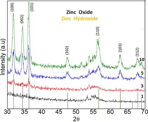
(3) ___________________________________________________________________________________________ Microscopy and imaging science: practical approaches to applied research and education (A. Méndez-Vilas, Ed.). When an excess of NH4OH is added to the solution, ammonia dissolves the hydroxide thus forming a transparent solution of two different chemical species as showed in Equations (2-3). Zn(OH)2 + 3NH4OH [Zn(NH3)4]2+ + 2H2O + OHZn(OH)2 + 2OH- [Zn(OH)4]2-. (2) (3). Equations (4) and (5) show the reaction when these complexes are heated around 80 ºC, forming ZnO. [Zn(NH3)4]2+ +2OH- ZnO + H2O + 4NH3 Zn(OH)42- ZnO + H2O + 2OH-. (4) (5). Among the most important experimental parameters that can influence this deposition process and the film quality, are the molar ratio of Zn:NH4OH, the duration of the reaction in hot water, and the drying process. Four processes are needed for a full deposition cycle: the adsorption of zinc–ammonia complex on the substrate, the formation of Zn(OH)2, the ultrasonic rinsing of substrate to remove counter-ions and loosely bonded Zn(OH)2, and the immersion of substrate in hot water to convert Zn(OH)2 to ZnO. 3.2. Structure and morphology. X-ray diffraction patterns (XRD) for each film with 1, 3, 5 and 10 cycles are shown in Fig. 1. XRD patterns for the films with 5 and 10 cycles showed three main peaks located at 31.8, 34.5 and 36.3°, corresponding to the planes (100), (002) and (101), respectively. All the observed peaks are attributed to the hexagonal wurtzite ZnO according to the JCPDS card 01-075-0576 (Joint Committee on Powder Diffraction Standards). When cycle number is less than 5, we observe a poor formation of ZnO over the surface; but after 5 cycles, the thin film starts growing. An improvement in the crystallinity of thin films is perceptible when the number of cycles increases due to a higher density and continuous growing over the substrate. Our thin films resulted polycrystalline with the main reflections (100), (101), (002) appearing, and all those indicated in the XRD spectra for thicker samples. Samples were also single-phase since no secondary phases were detected. Masashi Ohyama et al., reports that preferential orientation occurs depending of the precursor nature and suggests that solvents with low boiling points difficult the preferential orientation in the thin film growth [30]. The ZnO structures showed good crystallinity even when they were synthesized at low temperature.. Fig. 1 XRD patterns for ZnO thin films with 1, 3, 5 and 10 cycles number deposited by SILAR method.. 433.
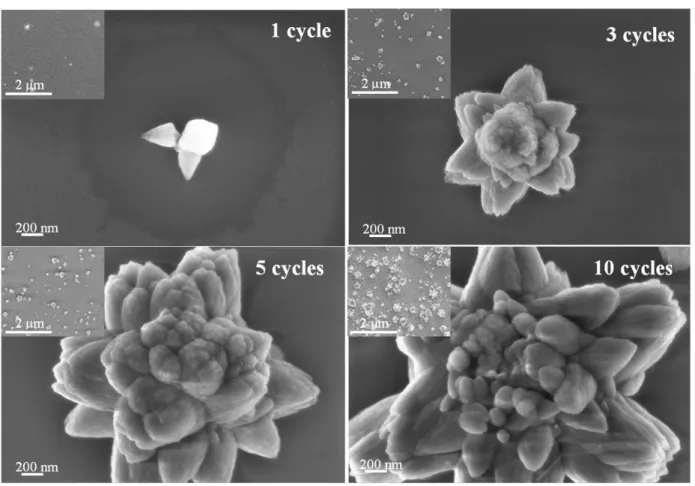
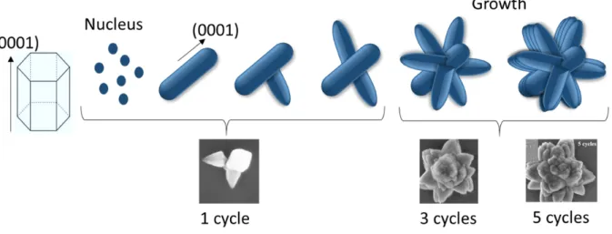
(4) ___________________________________________________________________________________________ Microscopy and imaging science: practical approaches to applied research and education (A. Méndez-Vilas, Ed.). Figure 2 shows typical FE-SEM images of the as-synthesized ZnO films. Several morphologies when depositing with different number of cycles were found. The distribution of the nanostructures in the surface is shown as an inset in each micrograph; an increment of the number of particles, size and a denser distribution was observed when the number of cycles was increased. In the 1 cycle sample, a bottom of around 320 nm of diameter accompanied by two petals of around 200 nm long and 250 nm wide were identified. Samples with a single deposit cycle exhibit few and small particles distributed on the substrate surface which reveals the nucleation stage for the ZnO growth. Also, a zone with very small grains is presented around the halo observed for 1 cycle sample and could be part of the ZnO growth. It is supposed that these particles have a larger surface energy compared to glass as confirmed at the sample with 3 cycles of deposition. For this condition, the aggregated particles prefer to grow in those already existing particles than on the uncovered surface. The continuous SILAR deposition up to 5 cycles reveals the structure evolution with a size of around 2.3μm with larger bottom and petals. The end particle size for 10 cycle deposition was 3μm. The flower-like microstructures consist of several leaf-like crystals (petals) with sharp ends radiating from the centre. These structures can be considered as cone-shaped particles that eventually transform into ZnO flower-like architectures. Even when the particles reach larger sizes at the end of 10 cycles, some small particles are still present. It is believed that the process occurs by the growth of large particles at the expense of smaller ones which dissolve (Ostwald ripening). This phase transformation process has been observed in a large number of systems where particles with different sizes are dispersed in a crystalline volume or matrix. The driving force of this process is the decrease in total surface free energy. At any stage during coarsening there is a so-called critical particle radius r∗ being in equilibrium with the crystalline volume; ZnO particles with r > r∗ will grow and ZnO particles with r < r∗ will shrink. The end point is a dispersion of precipitate particles embedded in the matrix, whose sizes vary depending on the nucleation rate of the precipitate. Because of the excess surface energy represented by the ZnO particulate ensemble, this condition does not satisfy the requirement of a minimum energy configuration. The system therefore continues to evolve to the state where the surface energy is lowered as much as possible. First, the ZnO nuclei are formed. Afterwards, the corners are produced as cones which are favorable for further nucleation and growth, and successive nanoparticles are adsorbed (cycle 1). New growth sites and nuclei are formed (cycle 3). Finally, the growth of units is carried out and the flower-like ZnO structure is obtained (cycle 5). Increasing the number of cycles to 10 provides a flower-like structure with greater number of petals, and a larger diameter.. Fig. 2 FE-SEM images of ZnO lily flower-like structures deposited by SILAR method at 90 °C and pH: 11.02.. The proposed growth mechanism of a lily flower-like ZnO structure is shown in Fig. 3. The polarity of some planes in the ZnO structure has been described by some research groups [31-33]. Considering this argument there are positive. 434.
(5) ___________________________________________________________________________________________ Microscopy and imaging science: practical approaches to applied research and education (A. Méndez-Vilas, Ed.). and negative charges in the medium as Zn2+, OH- and Zn(OH)42- ions that adsorb in some planes depending of their polarity. The Zn(OH)42- and OH- ions are attracted to the positive polar planes (0001) of Zn2+[31], and the reaction established in Equation (5) is carried out. ZnO will preferably grow in the c-axis direction. The growth of the ZnO-rod along the positive planes is limited by the amount of NH3, which can react with the Zn2+ ions in the positive polar surface forming Zn(NH3)2+ complexes. If a large amount of NH3 reacts with Zn2+, the surface energy of this plane will be reduced, inhibiting the growth. Therefore, the process is carried out at the middle of this rod, with the six facets of hexagonal wurtzite crystal forming six petals.. Fig. 3 Growth mechanism of a ZnO lily flower-like structure prepared by SILAR method.. The growth of these structures is governed mainly by the pH and the [OH-] /[Zn2+] molar ratio. The several morphologies and sizes of ZnO structures obtained are strongly influenced by these two factors. Therefore, the effect of pH on the morphology of the structures was studied. In Fig. 4 the morphologies for different deposits made at pH 9.36, 10.25 and 10.62 are shown. When the deposit is made under pH 10.25, there is an inhibition for the formation of the flower-like ZnO structure; it could be observed that the particles grow in rice-shaped or bicone-like structures. When the pH increases to 10.62, there is coalescence of these particles causing a 3-dimensional structure arrangement.. Fig. 4 FE-SEM images of ZnO obtained at 90 °C and 10 deposit cycles at different pH.. Figure 5 shows the morphology of samples deposited at different temperatures. Deposits made at a temperature below 60 ° C exhibit a two-dimensional growth; a thin layer of ZnO can be observed on the substrate surface. The formation of different three-dimensional structures is favoured at a temperature of 70 ° C. The adopted morphology is very diverse when deposits are made at 70 and 80 ° C, not showing well-defined growth. The flower-like ZnO structures were obtained at a temperature of 90 ° C, where it can be seen that the bundles strongly resemble natural lily flowers.. 435.
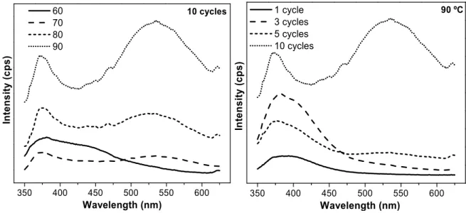
(6) ___________________________________________________________________________________________ Microscopy and imaging science: practical approaches to applied research and education (A. Méndez-Vilas, Ed.). Fig. 5 FE-SEM images of ZnO obtained at a pH: 11.02 and 10 deposit cycles deposited at different temperatures.. Fluorescence spectra of ZnO structures are characterized by an emission band close to the ultraviolet region and another wide emission band due to deep levels in the visible region. The width of this band results from the overlap of various deep light emitting levels that occur at the same time. Figure 6 shows the fluorescence spectra for the deposits at different temperatures and number of SILAR cycles. In the graphs it can be observed that the highest intensity comes from the samples deposited at a pH of 11.02 and a temperature of 90 ° C. These spectra are characterized by a band around 375 nm which can be attributed to exciton recombination. The wide band located in the region of 460-600 nm is attributed to surface defects, such as zinc vacancies or interstitial oxygen [34]. Samples deposited at a temperature below 70 ° C do not show luminescence in the visible region.. 60 70 80 90. 1 cycle 3 cycles 5 cycles 10 cycles. 90 ºC. Intensity (cps). Intensity (cps). 10 cycles. 350. 400. 450. 500. 550. 600. 350. Wavelength (nm). 400. 450. 500. 550. 600. Wavelength (nm). Fig. 6 Fluorescence spectra of ZnO deposited at different temperatures and number of cycles.. 4. Conclusions It was demonstrated that ZnO thin films with different kind of morphologies can be produced using Successive Ionic Layer Adsorption and Reaction (SILAR) method at low temperature. The effect of pH and cycle number influences the final morphologies. Lily flower-like morphologies are obtained when the cycle number increases from 1 to 10. Whenever pH is varied we find that ZnO growth is rice shaped, and while the pH is varied, we find that ZnO growth of in rice shaped. If the temperature is increased on the rinsing step from 60°C to 90°C, we find that the tips of the flowers are softer in shape than the tips of the flowers grown at room temperature. This kind of morphologies could be used in different applications because their surface area is larger than the conventional morphologies.. References [1] D.Y. Jiang, J.X. Zhao, M. Zhao, Q.C. Liang, S. Gao, J.M. Qin, Y.J. Zhao, A.Li. Optical waveguide based on ZnO nanowires prepared by a thermal evaporation process. Journal of Alloys and Compounds. 2012; 532: 31–33. [2] Deepak Bhatia, Himanshu Sharma, R.S.Meena, V.R.Palkar. A novel ZnO piezoelectric microcantilever energy scavenger: Fabrication and characterization. Sensing and Bio-Sensing Research. 2016; 9: 45–52.. 436.
(7) ___________________________________________________________________________________________ Microscopy and imaging science: practical approaches to applied research and education (A. Méndez-Vilas, Ed.). [3] Vithoba L.Patil, Sharadrao A. Vanalakar, Pramod S. Patil, Jin H. Kim. Fabrication of nanostructured ZnO thin films based NO2 gas sensor via SILAR technique. Sensors and Actuators B. 2017; 239: 1185–1193. [4] Chandan Biswas, Zhu Ma, Xiaodan Zhu, Toshiyuki Kawaharamura, Kang L. Wang. Atmospheric growth of hybrid ZnO thin films for inverted polymer solar cells. Solar Energy Materials & Solar Cells. 2016; 157: 1048 –1056. [5] Astrid Bingel, Martin Steglich, Philipp Naujok, Robert Müller, Ulrike Schulz, Norbert Kaiser, Andreas Tünnermann. Influence of the ZnO:Al dispersion on the performance of ZnO:Al/Ag/ZnO:Al transparent electrodes. Thin Solid Films. 2016; 616: 594-600. [6] Haixia Chen, Jijun Ding, Xiaomeng Wang, Xiaojun Wang, Guoxiang Chen, Li Ma. Enhanced mechanism investigation on violetblue emission of ZnO films by incorporating Al and Zn to form ZnO-Al-Zn films. Optical Materials. 2016; 62: 505-511. [7] Yuping Zhao, Chengchen Li, Mingming Chen, Xiao Yu, Yunwei Chang, Anqi Chen, Hai Zhu, Zikang Tang. Growth of aligned ZnO nanowires via modified atmospheric pressure chemical vapor deposition. Physics Letters A. 2016; 380: 3993–3997. [8] Yichun Ding, Fan Zheng, Zhengtao Zhu. Low-temperature seeding and hydrothermal growth of ZnO nanorods on poly(3,4ethylene dioxythiophene):poly(styrene sulfonic acid). Materials Letters. 2016; 183: 197-201. [9] Sunghoon Park. High-response and selective hydrogen sensing properties of porous ZnO nanotubes. Current Applied Physics. 2016; 16: 1263-1269. [10] ZnO sheets prepared with a light-assisted growth method for improved photodegradation performance. Xuewen Wang, Yuanquan Miao, Wuyou Wang, Gang Feng, Rongbin Zhang. Journal of Energy Chemistry. 2016; 25: 636-640. [11] Feifei Wang, Ruibin Liu, Anlian Pan, Sishen Xie, Bingsuo Zou. A simple and cheap way to produce porous ZnO ribbons and their photovoltaic response. Materials Letters. 2007; 61: 4459–4462. [12] Bingqian Han, Xu Liu, Xinxin Xing, Nan Chen, Xuechun Xiao, Shuyang Liu, Yude Wang. A high response butanol gas sensor based on ZnO hollow spheres. Sensors and Actuators B. 2016; 237: 423–430. [13] Arpita Jana, N.R. Bandyopadhyay, P. Sujatha Devi. Formation and assembly of blue emitting water lily type ZnO flowers. Solid State Sciences. 2011; 13: 1633-1637. [14] Wang Y, Li X, Wang N, Quan X, Chen Y. Controllable synthesis of ZnO nanoflowers and their morphology-dependent photocatalytic activities. Separation and Purification Technology. 2008; 62 (3): 727-32. [15] Zhixiang Ye, Ting Wang, Shuang Wu, Xiaohong Ji, Qinyuan Zhang. Na-doped ZnO nanorods fabricated by chemical vapor deposition and their optoelectrical properties. Journal of Alloys and Compounds. 2017; 690: 189-194. [16] Z. Shaban, M.H. Majles Ara, S. Falahatdoost, N. Ghazyani. Optimization of ZnO thin film through spray pyrolysis technique and its application as a blocking layer to improving dye sensitized solar cell efficiency. Current Applied Physics. 2016; 16: 131134. [17] Saâd Rahmane, Mohamed Salah Aida, Mohamed Abdou Djouadi, Nicolas Barreau. Effects of thickness variation on properties of ZnO:Al thin films grown by RF magnetron sputtering deposition. Superlattices and Microstructures. 2015; 79: 148-155. [18] A. Zaier, A. Meftah, A.Y. Jaber, A.A. Abdelaziz, M.S. Aida. Annealing effects on the structural, electrical and optical properties of ZnO thin films prepared by thermal evaporation technique. Journal of King Saud University – Science. 2015; 27: 356-360. [19] Reyhaneh Bahramian, Hossein Eshghi, Ahmad Moshaii. Influence of annealing temperature on morphological, optical and UV detection properties of ZnO nanowires grown by chemical bath deposition. Materials and Design. 2016, 107: 269-276. [20] C.M. Mbulanga, Z.N. Urgessa, S.R. Tankio Djiokap, J.R. Botha, M.M. Duvenhage, H.C. Swart. Surface characterization of ZnO nanorods grown by chemical bath deposition. Physica B. 2016; 480: 42-47. [21] S.C. Shei, P.Y. Lee. Influence of rinsing temperature on properties of ZnO thin films prepared by SILAR method with propylene glycol. Journal of Alloys and Compounds. 2013; 546: 165-170. [22] K. Ravichandran, P.V. Rajkumar, B. Sakthivel, K. Swaminathan, L. Chinnappa. Role of precursor material and annealing ambience on the physical properties of SILAR deposited ZnO films. Ceramics International. 2014; 40: 12375-12382. [23] Y.F. Nicolau, Solution deposition of thin solid compound films by a successive ionic-layer adsorption and reaction process, Applications of Surface Science. 1985; (22-23): 1061-1074 [24] Alyamani A, Lemine O. FE-SEM Characterization of Some Nanomaterial: INTECH Open Access Publisher; 2012 [25] Zhou W, Apkarian R, Wang ZL, Joy D. Fundamentals of Scanning Electron Microscopy (SEM). Scanning Microscopy for Nanotechnology. Springer. 2006; 1-40. [26] Reichelt R. Scanning Electron Microscopy. In: Hawkes PW, Spence JCH, editors. Science of Microscopy. New York, NY: Springer New York. 2007; 133-272. [27] Dufek M. Nova NanoSEM User Operation Manual. In: FEI C, editor. 2008. [28] FEI. Nova-NanoSEM data sheet: FEI Company; 2016 [cited 2016 November 06] https://www.fei.com/products/sem/novananosem/]. [29] S.B. Jambure, S.J. Patil, A.R. Deshpande, C.D. Lokhande. A comparative study of physico-chemical properties of CBD and SILAR grown ZnO thin films. Materials Research Bulletin. 2014; 49: 420-425. [30] Masashi OHYAMA, Hiromitsu KOZUKA, Toshinobu YOKO, Sumio SAKKA, Preparation of ZnO films with preferential orientation by Sol-Gel method, Journal of Ceramic Society of Japan. 1996; 104: 296-300. [31] R. Al-Gaashani, S. Radiman, A.R. Daud, N. Tabet, Y. Al-Douri. XPS and optical studies of different morphologies of ZnO nanostructures perpared by microwave methods. Ceramics International. 2013; 39: 2283–2292. [32] Juan Xie, Ping Li, Yanji Wang, Yu Wei. Synthesis of needle-and flower like ZnO microstructures by a simple aqueous solution route. Journal of Physics and Chemistry of Solids. 2009; 70: 112-116. [33] Ping Li. Hui Liu, Yang-Feng Zhang, Yu Wei, Xin-Kui Wang. Synthesis of flower-like ZnO microstructures via a simple solution route. Materials Chemistry and Physics. 2007; 106: 63-69. [34] Magnus Willander, Omer Nur, Jamil Rana Sadaf, Muhammad Israr Qadir, Saima Zaman, Ahmed Zainelabdin, Nargis Bano and Ijaz Hussain. Luminescence from zinc oxide nanostructures ad polymers and their hybrid devices. Materials. 2010; 3: 2643 – 2667.. 437.
(8)
Figure
Documento similar
Zuyi, Use of the ion exchange method for the determination of stability constants of trivalent metal complexes with humic and fulvic acids II. y otros cuatro autores, Adsorption
Solar cells with the CZTS absorber layers annealed at different heating rates were fabricated by using a CdS buffer layer deposited by chemical bath
It is well-known that the addition of salting-out species to aqueous media, like inorganic or organic salt ions, leads to a decrease on the solubility of hydrophobic ILs in water
A detailed kinetic study on the adsorption of the hydrophobic ionic liquid 1-methyl-3- octilimidazolium hexafluorophosphate (OmimPF 6 ) onto three commercial and
To sum up, by means of a simple method, in a single step at room temperature based on the high insolubility in the reaction medium of the PCs 1 and 2, we can control the
Validation is an important feature in any method of measurement because it is closely related to the quality of the results. A method of analysis is characterised by its
Again, as in Takada's method, ELL (efficient) identification in the limit is possible by using a regular language (efficient) identification method, and this requires the
Importantly, this alkenylation method seems to be not very sensitive to steric hindrance imposed by aryl ortho-substitution, as illustrated in smooth reaction
