Thermomechanical degradation of single and multiple quantum
well AlGaAs/GaAs laser diodes
J.Soutoa, J.L.Puraa, A.Torresa, J.Jiméneza,*
aGdS Optronlab, Ed. LUCIA, Paseo de Belén, s/n, Universidad de Valladolid, 47011
Valladolid, Spain
Abstract
The catastrophic degradation of laser diodes with active zones comprising either single (SQW) or multiple quantum wells (MQW) has been analysed via finite element methods. This analysis is based on a physical model that explicitly considers the thermal and mechanical properties of the diode laser structure and the relevant size effects associated with the small thickness of the active layers of the device. The reduced thermal conductivities and the thermal barriers at the interfaces result in a significant local heating process which is accentuated as more quantum wells form the active part of the device. Therefore, in the design of high power devices, the SQW configuration would be more appropriate than the MQW alternative.
Keywords
Laser diode, catastrophic optical damage, thermal conductivity, single quantum well, multiple quantum wells, finite element methods
1. Introduction
The optical output power of high power laser diodes is limited by the catastrophic optical damage (COD). The mechanisms driving this degradation must be understood in order to increase the power and lifetime of laser diodes [1–3]. COD is a sudden drop of the optical power associated with a thermal runaway process in which the active part of the laser is locally destroyed. The endurance of the lasers to COD depends on the materials that form the laser, but it should also be influenced by the structure of the active zone. A laser diode is a multilayer structure in which the active zone is formed by one or more quantum wells (QW) with their corresponding barrier layers. The low dimensionality of these layers has an important impact in the behaviour of the active parts of the laser during operation.
First, one should mention that COD starts by a temperature increase in a tiny region of the active zone as a consequence of non-radiative recombination. This is the most probable source of local heating in the front facet, while local heating in the inner cavity may be produced by current crowding at defect rich regions. Independently of the original source of the initial heating, the evolution of the degradation depends on the laser structure. The subsequent response to the local heating is crucial to establish the endurance of the different laser structures.
The use of QWs was a step forward in the improvement of the optical power and reliability of diode lasers. The advantages of QW active regions are lower threshold currents, and also lower optical loads in the active zone. This is due to the fact that the active QW and the waveguide are decoupled, as compared to double heterostructure (DH) lasers, in which they are overlapped [4]. The use of active zones formed by multiple quantum wells (MQW) permits to further lower the threshold current [5]; however, high power lasers are preferentially done with single QW (SQW) active regions, because of their higher resilience to degradation at the power levels at which this type of lasers operate.
diode by means of a thermomechanical model in which the local heating is responsible for laser self-absorption and subsequent mechanical failure. This process leads to large temperature gradients that give rise to relevant thermal stresses. The temperature gradient was found to depend on the thermal conductivity of the laser structure. It should be noted that the nanometric thickness of the QW effectively reduces the thermal conductivity of that layer. Besides, one has to consider the presence of thermal boundary resistances at the interfaces. This structure brings about very local temperature increases, especially at the QW. A local temperature enhancement does not necessarily have fatal consequences unless a critical temperature is reached. This critical temperature is related to the formation of dislocations in the active zone of the laser. The thermal runaway process is associated with the propagation of those defects and the destruction of the laser cavity assisted by the optical absorption. As a result of that deterioration, melting temperatures can be eventually reached. Based on that model, we analyse herein the thermomechanical behaviour of the active zones in AlGaAs/GaAs MQW lasers.
2. Laser structure and modelling
High power single SQW and MQW AlGaAs (808 nm) edge emitter lasers were studied. We have rationalized the problem assuming that, as a result of the continuous operation of the device, a local heating source is generated in the active zone of the laser, most specifically in the QW (or in one of the QWs for MQW devices). This is the most likely situation, since the QWs are the laser absorbing media, while the barrier layers are transparent to the laser radiation. In order to consider the most unfavorable conditions in terms of heat management, the source (absorbing region) has been placed at the laser facet. The structures of the different laser diodes modelled in this work are outlined in Table 1.
Thickness (m) x in AlxGa1-xAs
150 CuW (heat sink)
3 AuSn (soldering)
0.12 0
0.05 0.55 → 0
0.89 0.55
0.08 0.65 → 0.55
0.5 0.65
0.13 0.26 → 0.65
0.012 (QW) 0.1
0.01 (separation layer) 0.26
0.012 (QW) 0.1
0.13 0.65 → 0.26
0.5 0.65
0.08 0.55 → 0.65
1 0.55
1.5 0 → 0.55
130 0
The physical properties of the different materials that form the laser structure are listed in Table 2 [8–16]. The temperature dependence of the parameters has been explicitly considered for the numerical simulations. For those properties of the ternary alloys with significant contributions arising from lattice disorder, corrections are introduced via the Vegard’s law, with the corresponding bowing parameter [9].
Physical property GaAs AlAs
α (K-1) 4.24·10-6+5.82·10-9T-2.82·10-12T2 2.736·10-6+7.943·10-9T
(W/K m) -9.19+3.17·10-3T+1.61·10-4T-1 -2.27+8.16·10-3T+2.95·104T-1 C11 (Pa) 1.217·1011-1.44·107T 1.193·1011
C12 (Pa) 5.46·1010-6.4·106T 5.75·1010 C44 (Pa) 6.16·1010-7.0·106T 5.66·1010
Physical property AuSn CuW
α (K-1) 1.59·10-5 7.3·10-6
(W/K m) 57.3 198
ν 0.30 0.29
E (Pa) 5.3·109+4.39·108T-8.67·105T2 3.1·1011
Table 2. Main physical parameters of the materials used for the computations: α, thermal expansion coefficient; , thermal conductivity; C11, C12 and C44, elastic constants; ν, Poisson ratio; and E, Young’s modulus.
The temperature and stress distributions were solved by finite element methods using the commercial software COMSOL®. The temperature distribution in the device is calculated by solving the heat transfer equation under the assumption that the heat is generated at a tiny region of the QW; note that we are not dealing with the junction temperature, but with a localized hot spot. Thermal boundary conditions are set as a fixed temperature for the upper surface of the heat sink, and as convective and radiative cooling for the remaining walls of the laser.
In order to study the mechanical counterpart, the thermal solution is the input for the thermomechanical equation, which is thereafter solved. Thermal strains are calculated at each point of the structure considering the thermal expansion coefficients, and are subsequently connected to the generated mechanical stresses via the constitutive equation in which the elastic constants for each material in the laser structure are specified. Free displacement conditions were set for all the surfaces except for the bottom of the substrate, for which translation and rotation movements were excluded.
In a series of recent works [17,18], we have reported about the marked influence that the nanoscale dimensions of the active parts of QW laser diodes have on the degradation process. Poorer thermal conductivity figures, as well as the presence of thermal barriers at the interfaces, gave rise to local temperatures higher than those that would have been expected if bulk thermal transport figures had been considered. In those works, a range of values for the effective thermal conductivity (eff) versus bulk conductivity (bulk)
factor were studied, and their relevance in the route to COD was studied. Here, a conservative factor, effbulk=0.25, is used throughout. On the other hand, mechanical
influence of the number of quantum wells in a laser diode, and its impact on the device reliability.
3. Temperature distribution
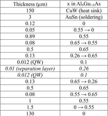
The thermal profiles calculated for different laser diodes are shown in Figure 1. These plots are focused on the central layers (QWs, separation layers and guides) of the laser structures, where a notable rise in the temperature is estimated. This heating effect is strictly local, so that the temperature in the substrate and the heat sink remains almost unaltered at 303 K, and the junction temperature out of the region under the influence of the local heating corresponds to the operational condition of the device [7]. The z axis of the graph corresponds to the epitaxial growth direction, and the origin has been set at the centre of the specific QW where the heat source is placed. The size of the sources (1 m sideways, and the whole thickness of the QW) and the power densities absorbed (10 MW/cm2) are identical for the three cases here illustrated. This power density corresponds to the laser radiation absorbed by the locally heated region, and the total energy accumulated is balanced by the heat dissipation mechanisms described above.
It can be clearly appreciated that the presence of two quantum wells results in a very significant increase of the peak temperature at the core of the heat source, when compared to the SQW configuration (820 vs 710 K). Including additional quantum wells and separation layers in the structure leads to even higher maximum temperatures (about 1000 K for five quantum wells).
Figure 1. Thermal profiles for the active layers at the laser facet along the growth direction for devices with 1, 2 and 5 QWs. The heat source is placed in the layer furthest from the heat sink for the 2 QWs case, and at the central QW for the 5 QWs configuration.
dissipation is severely reduced when the overall thermal conductivity is limited by the presence of several interfaces with their corresponding thermal boundary resistances.
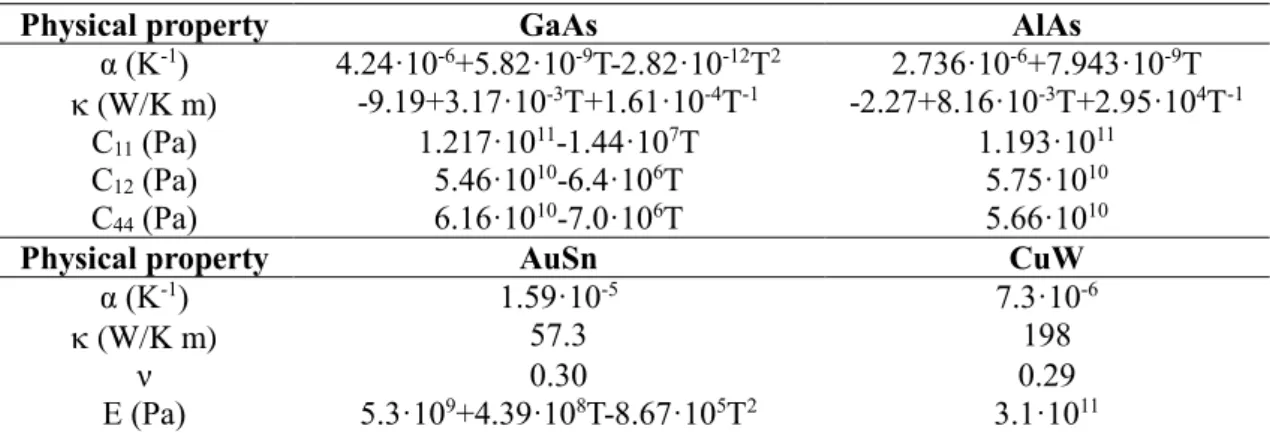
The peak temperature for the 5 QW laser depends notably on the particular QW where the laser radiation is absorbed. This is illustrated in Figure 2, where the temperature profiles for a power density of 12 MW/cm2 are plotted for all the possible positions of the heat source. If the heat is generated in the central (3rd) QW, a peak temperature of 1230
K is estimated. This value is significantly lower if the heat spot is located in the outer QWs. The maximum temperature, both for the QW closest to the substrate (1st) and for the one closest to the heat sink (5th), is approximately 1035 K. If the heat source is placed
in either of the intermediate QWs (2nd or 4th), a local value of about 1200 K would be reached. Therefore, as the number of thermal barriers that surround the heat source increases, the peak temperature concomitantly rises. This effect is particularly acute when comparing the figures for sources on the outer positions of the active layers with those for inner QWs. Hence, COD in MQW laser diodes is much more likely to be triggered by laser absorbing regions in the inner QWs. As it can be appreciated in the figure, the shapes of the curves also differ due to the dissimilar arrangement of the thermal barriers for the various locations of the heat source. Markedly asymmetrical temperature profiles are found when the source is placed in either of the edges, for which the thermal barriers are very unevenly distributed, while the opposite is found for the hot spot in the central QW.
Figure 2. Thermal profiles for a diode laser with 5 QWs. The heat source is alternatively placed in each of the five QWs. The origin for the horizontal axis corresponds to the midpoint of the central QW.
Figure 3. Peak temperatures in laser diodes with one, two, and five quantum wells as a function of the heating power density. The positions of the heat sources are those specified in Figure 1.
4. Thermal stresses
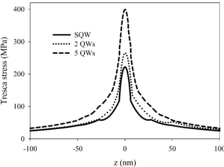
Figure 4. Thermal stresses across the active layers of the device for laser diodes with one, two and five QWs for a power density of 10 MW/cm2. Heat source dimensions and positions correspond to those described for Figure 1.
This trend can be clearly observed if one plots the calculated maximum Tresca (shear) stresses versus the peak temperature in the facet for the laser diodes here considered. As illustrated in Figure 5, the correlated data are distributed in all cases roughly along the same straight line regardless of the specific characteristics of the lasing structure. This agrees well with our description of the stresses being fundamentally originated by the temperature gradients around the overheated region.
Within our model, the COD is prompted as a critical temperature is reached. That temperature relates to the conditions under which dislocations are generated due to the thermal stresses. From a mechanical viewpoint, the onset of the COD process would occur at the crossing of the calculated Tresca stress – peak temperature data and the experimental curve for the yield strength of GaAs. Bearing the mechanical strengthening of nanoscale structures in mind, the experimental curve should be corrected for that effect. That would correspond to a shift of the bulk curve towards higher stresses. For the type of structures here considered, we estimated that the onset for plastic deformation approximately corresponds to a peak temperature of 600K [6,7]. For a SQW laser, that temperature is reached for absorbed laser powers of about 8 MW/cm2, according to Figure
5. For a device with 2 QWs, the power density required to set the COD would be slightly over 6 MW/cm2. If the configuration with 5 QWs is considered, the process would be triggered by a heat source of 5 MW/cm2. Therefore, from the standpoint of the robustness of the devices, the use of SQW lasers would be preferable for high power applications.
5. Conclusions
The correlation between the number of active quantum wells in AlGaAs/GaAs laser diodes and the thermal management of the device has been evaluated. A clear deterioration of the heat dissipation from the lasing layers is observed as the number of quantum wells is increased, which has deleterious consequences for the resilience of MQW lasers. The analysis of the thermomechanical stresses generated in the structure further support the use of SQW devices for high power applications.
Acknowledgements
This work was funded by the Spanish Government (ENE2014-56069-C4-4-R) and Junta de Castilla y León (VA293U13 and VA081U16 (003)). J. L. Pura was granted by the FPU programme of the Spanish Government (FPU14/00916).
References
[1] J.W. Tomm, J. Jiménez, Quantum Well Laser Array Packaging, McGraw-Hill, New York, 2006.
[2] D.F. Welch, A Brief History of High-power Semiconductor Lasers, IEEE J. Sel. Top. Quantum Electron. 6 (2000) 1470–1477. doi:10.1109/2944.902203.
[3] P.G. Eliseev, Optical strength of semiconductor laser materials, Prog. Quantum Electron. 20 (1996) 1–82. doi:10.1016/0079-6727(95)00002-X.
[4] O. Svelto, Principles of Lasers, Springer US, Boston, MA, 2010. doi:10.1007/978-1-4419-1302-9.
[5] T. Numai, Fundamentals of Semiconductor Lasers, Springer-Verlag, 2015. doi:10.1007/b97531.
[6] J. Souto, J.L. Pura, J. Jiménez, Nanoscale effects on the thermal and mechanical properties of AlGaAs/GaAs quantum well laser diodes: influence on the
catastrophic optical damage (COD), J. Phys. D. Appl. Phys. (2017). doi:10.1088/1361-6463/aa6fbd.
temperature for catastrophic optical damage in high power quantum well laser diodes, Laser Phys. Lett. 13 (2016) 25005. doi:10.1088/1612-2011/13/2/025005. [8] S. Adachi, Lattice thermal resistivity of III-V compound alloys, J. Appl. Phys. 54
(1983) 1844–1848. doi:10.1063/1.332820.
[9] S. Adachi, GaAs, AlAs, and AlxGa1−xAs: Material parameters for use in research and device applications, J. Appl. Phys. 58 (1985) R1–R29. doi:10.1063/1.336070.
[10] S. Adachi, Lattice thermal conductivity of group-IV and III-V semiconductor alloys, J. Appl. Phys. 102 (2007) 63502. doi:10.1063/1.2779259.
[11] M. Krieger, H. Sigg, N. Herres, K. Bachem, K. Köhler, Elastic constants and Poisson ratio in the system AlAs-GaAs, Appl. Phys. Lett. 682 (1995) 682. doi:10.1063/1.114098.
[12] S. Gehrsitz, H. Sigg, N. Herres, K. Bachem, K. Köhler, F. Reinhart,
Compositional dependence of the elastic constants and the lattice parameter of AlxGa1-xAs, Phys. Rev. B. 60 (1999) 11601–11610.
doi:10.1103/PhysRevB.60.11601.
[13] Y.A. Burenkov, Y.M. Burdukov, S.Y. Davidov, S.P. Nikanorov, Temperature dependences of the elastic constants of gallium arsenide, Sov. Phys. Solid State. 15 (1973) 1175–1177.
[14] O. Madelung, W. von der Osten, U. Rössler, Intrinsic Properties of Group IV Elements and III-V, II-VI and I-VII Compounds, Landolt-Börnstein Series, Springer-Verlag, Berlin, 1987.
[15] V.M. Glazov, A.S. Pashinkin, Thermal expansion and heat capacity of GaAs and InAs, Inorg. Mater. 36 (2000) 225–231. doi:10.1007/BF02757926.
[16] W. Martienssen, H. Warlimont, eds., Springer Handbook of Condensed Matter and Materials Data, Springer-Verlag, Berlin, 2005.
[17] V. Hortelano, J. Anaya, J. Souto, J. Jiménez, J. Perinet, F. Laruelle, Defect signatures in degraded high power laser diodes, Microelectron. Reliab. 53 (2013) 1501–1505. doi:10.1016/j.microrel.2013.07.071.
[18] J. Souto, J.L. Pura, A. Torres, J. Jiménez, M. Bettiati, F.J. Laruelle, Sequential description of the catastrophic optical damage of high power laser diodes, in: Proc. SPIE, 2016: p. 973306. doi:10.1117/12.2212953.
[19] W.W. Gerberich, J. Michler, W.M. Mook, R. Ghisleni, F. Östlund, D.D. Stauffer, R. Ballarini, Scale effects for strength, ductility, and toughness in “brittle”
materials, J. Mater. Res. 24 (2009) 898–906. doi:10.1557/jmr.2009.0143. [20] T. Zhu, J. Li, Ultra-strength materials, Prog. Mater. Sci. 55 (2010) 710–757.