Switching of ferroelectric liquid crystal
doped with cetyltrimethylammonium
bromide-assisted CdS nanostructures
Kaushik Pal , Uday Narayan Maiti , Tapas Pal Majumder ,
Subhas Chandra Debnath , Sharmistha Ghosh , Subir Kumar Roy and
José Manuel Otón
Abstract
Large scale high yield cadmium sulfide (CdS) nanowires with uniform diameter were synthesized using a rapid and simple solvo-chemical and hydrothermal route assisted by the surfactant cetyltrimethylammonium bromide (CTAB). Unique CdS nanowires of different morphologies could be selectively produced by only varying the concentration of CTAB in the reaction system with cadmium acetate, sulfur powder and ethylenediamine. We obtained CdS nanowires with diameters of 64-65 nm and lengths of up to several micrometers. A comparative study of the optical properties of ferroelectric liquid crystal (FLC) Felix-017/100 doped with 1% of CdS nanowires was performed. Response times of the order of from 160 to 180 /xs, rotational viscosities of the order of from 5000 to 3000 mN s m~2 and polarizations of the order of from 10 to 70 nC c m- 2 were measured. We also observed an anti-ferroelectric to ferroelectric transition for CdS doped FLC instead of the ferroelectric to paraelectric transition for pure FLC.
(Some figures may appear in colour only in the online journal)
1. Introduction
Quasi-one-dimensional nanostructure materials, such as nanowires and/or nanotubes, have been successfully synthe-sized and have received much attention because of their interesting physical properties and potential applications in nanodevices [1]. In recent years, synthesis of one-dimensional semiconductor materials such as nanowires, nanorods and fibers has been the focus of a number of research works [2-5]. CdS is one of the most important II-VI semiconductors. It is a direct-band semiconductor with a band gap of 2.4 eV. CdS has vital optoelectronic applications for laser light emitting diodes and optical devices based on nonlinear properties [6]. As CdS is an important II-VI semiconductor
material, CdS nanocrystals have received considerable interest from researchers regarding the control of its morphology and size. Various approaches, such as the solvothermal route [7-9], a liquid crystal template, [10] irradiation [11,
12], polymer controlled growth [13] and electrodeposition on a porous template [14] have been applied to achieve one-dimensional CdS nanocrystals. Unfortunately, most of the reported nanowires have been very short, usually tens to several hundred nanometers in width and also in length. However, as we show in this work, it is possible to create nanowires having uniform lengths and widths with high yield in a facile unique strategy by the assistance of cetyltrimethylammonium bromide (CTAB).
(FLCs), with the aim of improving their response in order to enhance their behavior in display and optoelectronics devices. It is essential to obtain stable and uniform alignment of liquid crystals (LCs) on a macroscopic scale for the fabrication of high-quality liquid crystal displays (LCDs). Typically, alignment involves the modification or conditioning of a solid substrate such that its interface with the LC has some anchoring action that results in either planar (tangential) or homeotropic (perpendicular) orientation of the LC director (symmetry axis) with respect to the interface. Such conditioning is carried out on a substrate having an electrically conductive layer (usually indium tin oxide (ITO) or ITO-coated glass) for electric-field-induced reorientation of the director which, in turn, results in a variation in the transmitted light intensity. Currently, the preferred conditioning technique is rather primitive. The conductive substrate is coated with a polyimide layer that is mechanically rubbed [15, 16] after thermal curing. The alignment mechanism associated with unidirectional rubbing has contributions from both the physical grooves caused by rubbing the polyimide substrate, with the cost of the elastic energy related to conformably wetting the irregular substrate topography [15] and, secondly, putative molecular interactions between exposed polyimide functionalities and the LC. However, the details of LC alignment are not well understood [15, 17-19]. Thus, the search for more easily quantified alignment materials continues. The phase sequence of FLC Felix-017/100 mixture (Clairant, Frankfurt, Germany) is given by the following [20-22].
Cr < • SmC* •* • SmA* < • N* •* • Iso -28°C 73°C 77°C 85°C
One-dimensional (ID) nanostructured materials doped with ferroelectric liquid crystals [23] are being intensively investigated because they impart remarkable improvement in the physical parameters of the host materials [24-32]. Novel functionalities are elicited depending upon the optical and electrical properties of the nanomaterials and the interaction of the nanomaterials with the orientational field of the liquid crystals. The Freedericksz threshold voltage, residual DC, driving voltages, etc are found to decrease in carbon nanotube or semiconducting nanorod driven nematic liquid crystals [27-29, 31]. Metal nanoparticles protected with ligand molecules introduced into a nematic liquid crystal host exhibit a frequency modulation response with a short response time of the order of milliseconds in twisted nematic geometry [32, 33]. Doping ferroelectric nanoparticles in nematic LC increases the order parameter and phase sequence temperature range of the LC due to the effective coupling of the spontaneous polarization of the nanoparticles with the LC director [34-36]. Recently, a few works on doping nanoparticles in ferroelectric liquid crystals (FLCs) have been carried out [37-39]. Since the discovery of surface stabilization of ferroelectric liquid crystals [39], they have been considered as good candidates for display applications owing to their fast response and bistability. However, commercial applications in displays demand further improvements of the physical properties of the FLCs to yield
better contrast, lower driving voltage and good alignment without chevron structures. Therefore, modification of the existing FLC by blending nanomaterials in it may be a prospective method to improve those properties. The use of semiconducting nanowires can improve the electro-optical properties of a ferroelectric liquid crystal. The improvements are significant in response time and rotational viscosity.
This study is directed at understanding the structure and physical properties of hydrogen bonded LC gels in freely suspended film geometry. The experiments include structural assessment by means of polarizing microscopy, electro-optical investigations and some accompanying spectroscopic measurements. We will discuss the influences of the network formed in the gelling process on the mesophase properties of the material, i.e. the stabilization of orientational states and the dynamics of the reorientation in electric fields, and on the mechanical properties such as shape distortions and the suppression of macroscopic flow in the films.
2. Experimental procedure
2.1. Synthesis
All the chemicals used in this work were of analytical grade and commercially available, and were used without further purification. The chemicals used, such as ethylenediamine (EDA), Cd(CH3COO)2-2H20, sulfur powder and CTAB, were purchased from Atlanta Drugs Chemical Reagent Co. Ltd (Sigma Aldrich and E Merck).
In a typical procedure, 0.66 g of Cd(Ac)2 and 0.075 g of sulfur (S) powder were placed in a 100 ml beaker, and were dissolved into 45% of ethylenediamine under vigorous stirring for 15 min. Then, 0.35 g of CTAB was added to the precursor and then stirred for 25 min. After a complete stirring using a magnetic stirrer (Remi), the final solution was placed in a 100 ml stainless steel coated Teflon-lined autoclave. The autoclave was placed in a heating chamber at 200 °C for 2 h. Finally, after cooling the autoclave naturally at room temperature, a strongly pungent bubble forming solution was produced. The resultant sample was filtered off and washed with deionized distilled water and ethanol several times until the impurity product was washed and separated away from the desired sample. The sample was dried out in a vacuum at 75 °C for 3 h. In order to study the influence of CTAB surfactant on the nanostructure formation, the original 0.35 g of CTAB was changed by repeating the same synthesis with 0.15 and 0.65 g of CTAB in a similar fashion.
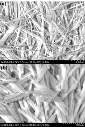
Figure 1. FE-SEM images of high yield uniform CdS nanowires evolved with the addition of CTAB (0.35 g) at a resolution of (a) 2 /xm and (b) 500 nm.
sheet on opposite sides of the hole served as electrodes. They provided the driving electric fields in the film plane. We studied the images of the films with a reflection microscope. All texture pattern images (maximum frame rate 25 frames s_ 1) were recorded with a Nikon Coolpix 990 CCD camera. They were subsequently contrast amplified and processed digitally. The films were observed with a crossed linear polarizer. However, since a number of optical elements are in the light path (e.g. a prism that splits the incident and reflected beams), the polarization of the incident light is not perfectly linear but slightly elliptical. This has to be considered in the discussion of optical image analysis through nano-doped liquid crystal phase changes with temperature.
2.2. Characterizations
Field emission scanning electron microscopy (FE-SEM) (model: Hitachi-FESEM, S4800-JU at 5.0 kV and SEM, JU-MET) was used to record the scanning electron micrograph for the morphological analysis of the nanostructures. The structures of the nanomaterials were investigated by using x-ray diffraction studies (XRD) with a diffractometer (model: Bruker D8 Advance) with the Cu Ka line. Preparation of the thin films were carried out by using a programmable spin coater (Apex Instruments Co., model: SCU-2008C) and the surface behavior with roughness of the thin films prepared in this way was studied by using atomic force microscopy (AFM) (model: Veeco, dilnnova). An
34300-JU 5.0kV5.9mm x90.0k SE
Figure 2. FE-SEM images of CdS nanoparticles evolved with the addition of CTAB (0.15 g) at a resolution of (a) 5 /xm, (b) 1 /xm and (c) 500 nm.
ultraviolet-visible scanning spectrophotometer (UV-2401PC, TCC-240A, Shimadzu, Japan) was used to record the electronic absorption spectra of the films at room temperature. The photoluminescence spectra were measured by using excitation of 325 nm from a He-Cd laser source (LS55, fluorescence spectrometer, PerkinElmer). The frequency dispersion electro-optical data were recorded at room temperature for frequencies ranging from 10 Hz to 13 MHz using a Hewlett Packard 4192A LF impedance analyzer and dc conductance measurements were made using a source meter (model: Keithley 2611A system).
For electro-optic measurement an HP 33120A signal generator and an HP 54603B oscilloscope were used. The spontaneous polarization (Ps) and the relaxation time were measured by using a polarization reversal method and calculated with the help of the following relation [30, 31]:
Figure 3. FE-SEM images of CdS nanogranules evolved with the addition of CTAB (0.65 g) at a resolution of (a) 5 /xm and (b) 2 /xm.
All measurements were computer based. The viscosity (y) was determined from the measured value of the polarization (Ps) and the switching time (r) using the following relation [30, 31]:
y
T = . (2)
1J5PSE
3. Results and discussion
3.1. Morphology analysis
The morphological confirmation of the different compositions of the CdS nanocomposite materials was performed using field emission scanning electron microscopy (FE-SEM). The experimental studies revealed that high yield large scale uniform CdS semiconductor nanowires with very uniform controllable morphological growth are synthesized using a unique solvothermal route with the addition of surfactant CTAB, as shown in figure 1. The results are significantly improved by using CTAB in comparison with previously reported [40] CdS nanostructures based on the surfactant polyethylene glycol (PEG) with various concentrations at different times and ambient conditions. In our earlier publication [41], we prepared CdS nanowires based on PEG surfactant with diameters in a range of the order of 31-36 nm and lengths in a range of the order of 354-360 nm. In this paper we have obtained CdS nanowires based on CTAB surfactant (0.35 g) having diameters of the order of 64-65 nm with lengths of the order of A3A-A13 nm. Interestingly enough, by adding a lower amount of CTAB (0.15 g), the
*
Figure 4. Atomic force microscopy (AFM) topography of as-prepared thin film for LC doped CdS nanowires (0.35 g CTAB concentration).
morphological structure of the CdS observed by SEM totally changed and the nanowires turned into nanoparticles with diameters of around 8-149 nm, as illustrated in figure 2. In addition to this, more interesting for this work is the result obtained at higher concentration (0.65 g). With the reaction of CTAB with ethylenediamine, conversion of CdS nanoparticles to nanogranule structures with a uniform diameter of 92 nm results, as confirmed in the higher resolution SEM imagee (figure 3(b)). This hydrothermal reaction takes place with ethylenediamine (en) acting as a solvent as well as a complexing agent. In our synthetic system, the investigation of CdS nanoparticle formation indicated that the nucleation and growth were well controlled. Firstly, ethylenediamine, as a strongly bidentating solvent, was ready to form relatively stable Cd2 + complexes [42-44]. Next, cadmium ions could combine with an ethylenediamine molecule (which acts as a bidentate ligand) to form a Cd-ethylenediamine complex ([Cd(en)2]2+) [42], which was stabilized in the solution. Meanwhile, S powder was dissolved in the ethylenediamine. Finally, due to the slow release of S2~ ions and the low free Cd2+ concentration (log ¿¡2 = 10.09, P2 is the stability constant of the complex ([Cd(en)2]2+)), the reaction rate is slow, which is in favor of oriented growth of the CdS nanowires [45].
O.EMm
c:
•a
Distance (nm)
S.4B 10.6 |jm
2SOO0 30000 3SOO0 40000 4 50 DO S30D3 5S00D 60000 05000 70000
Height (urn)
Figure 5. (a) A non-contact mode AFM image of LC doped CdS grain height profiles acquired at selected locations with distance, (b) The number density of grains plotted against height of the as-prepared thin film.
and the sample is homogeneously spread there. The average thickness of the thin film is 185 nm. A detailed investigation is also made through further analysis of the AFM characteristics (figure 5(a)). In addition to this, we can also determine LC doped CdS nanomaterial thin films which vary with height distributed in nanometer ranges and we are able to predict the number density of the molecule (LC doped CdS grain) distribution; these increases are exponentially plotted against height in several micrometer ranges which resulted after analysis in figure 5(b). The thickness and roughness have been increased remarkably due to the introduction of Felix, keeping the same rpm for both cases for the preparation of a single layer homogeneous dispersion of thin film.
3.2. Crystalline structure analysis
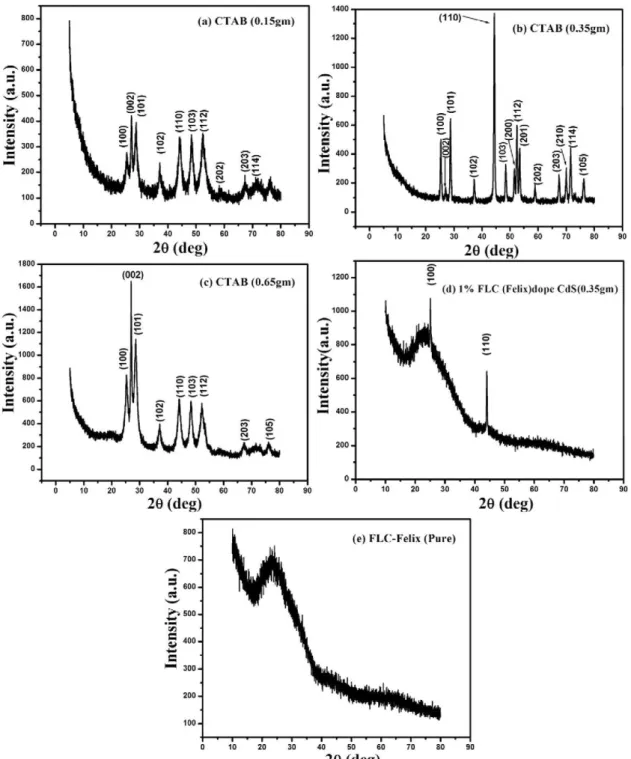
We recorded x-ray diffraction patterns (XRDs) of pure CdS nanostructures, pure Felix and CdS doped Felix by using an x-ray diffractometer with Cu Ka radiation (0.014 18 nm) at a scan rate of 0.05° s_ 1. Figure 6(b) shows the XRD pattern of the well crystalline synthesized CdS nanowires for the CTAB concentration of 0.35 g, with all the diffraction peaks corresponding to the hexagonal wurtzite phase of CdS. From this XRD pattern we obtained the crystal parameters of the sample. These matched well with those on the JCPDS
8 0 0 .
7 0 0
-«•—. 6 0 0 .
S
^ 5 0 0
-£» '
a
£
300-a
100-0 10 20
te
o a
^.
30 o
w
40
(a)CTAB(O.lSgm)
O «"ÍÑ*
T V r
5D
<N I y , J
T" • Jfll Ai
60 70 SO 9
1800.
1600.
1400.
^ 1200
>j1000.
'I 800.
"g 600.
—
400.
200
0
29 (deg)
10 20 30 40 50 26(deg)
(c) CTAB (0.65gm)
0 10 20 30 40 SO 60 70 00 26(deg)
0 10 20 30 40 50
29 (deg)
26(deg)
Figure 6. XRD crystalline pattern of different CdS nanostructures evolved with the addition of CTAB (a) 0.15 g, (b) 0.35 g, (c) 0.65 g, (d) Felix doped CdS nanowires (CTAB 0.35 g) and (e) pure FLC-Felix(017/100).
in figures 6(a)-(e) suggest that the obtained product is well crystallized. The d-spacing of the CdS nanowires was calculated using the XRD analysis and compared with the standard JCPDS data (table 1). The corresponding (hkl) values are given in the table.
3.3. Optical behavior
UV-visible spectroscopy was employed because of its simplicity, versatility, speed, accuracy and cost effectiveness. An obvious difference between certain compounds is their
Table 1. The comparison of ¿-values, obtained from X R D and JCPDS, and illustration of the corresponding (hkl) planes.
Peak
1 2 3 4 5 6 7 8 9 10 11 12 13
2(9° (deg)
25.04 26.78 28.57 37.07 43.88 48.08 51.3 52.09 53.3 69.5 69.93 71.3 76.27
d-XRD (Á)
3.5561 3.3289 3.1296 2.4251 2.0632 1.8924 1.8005 1.7557 1.7042 1.5803 1.7223 1.5503 1.9903
d-JCPDS (Á)
3.5861 3.3599 3.1630 2.4519 2.0705 1.8998 1.8054 1.7627 1.7098 1.5896 1.7228 1.5563 1.9985
(hkl)
100 002 101 102 110 103 200 112 201 203 210 114 105
due to FLC-Felix doped with uniform CdS nanowires (CTAB 0.35 g). In the case of photo-excitation, this luminescence is called photoluminescence. Photo-excitation causes electrons within a material to move into permissible excited states. When these electrons return to their equilibrium states, the excess energy is released and may include the emission of light (a radiative process) or may not (a non-radiative
250
e
a
£i - 150
C <
50
CTAB(.15gm) • CTAB(.35gm) •
CTAB(.65gm) —
T-CTAB(.35gm)+LC
—• 1 • — 550 600 650
X ( n m )
- 1 — 700
Figure 7. UV-visible absorption spectra of CdS nanostructures for various CTAB concentrations: (a) 0.15, (b) 0.35 and (c) 0.65 g; (d) Felix doped CdS nanowire (CTAB 0.35 g) thin film coating on a glass substrate.
process). The energy of the emitted light (photoluminescence) relates to the difference in energy levels between the two electron states involved in the transition between the excited
(a)Excitatinii.CTAB(.l 5«m) 325nm •
[512) (525) 3 5 0 n m - 375nm-
425nm-500 600
A.(nm)
500 S50 600 A. ( i n n ) (c)Excitation.CTAB(.65gm)
(52¿) 32!mm 350nm 375nm 5) 425nm
HO M0
X fnm) M u m )
(55°C)
Figure 9. Optical micrograph of texture variation with temperature, for (a) 25 °C, (b) 50 °C and (c) 55 °C, for an applied electric field on CdS nanowire (CTAB 0.35 g) doped FLC-Felix sandwiched and confined in ITO polished cells.
state and the equilibrium state. Figure 8 illustrates in detail photoluminescence studies in which we use 0.35 g of CTAB with a high intensity peak maximum mostly occurring in the 521 nm region with shoulder peaks in both the red and blue shift regions, as depicted in figure 8(b). At lower concentration of CTAB (0.15 g), the peak intensity reduces in the wavelength region of 525 nm, with shoulder peaks on both sides, as shown in figure 8(a). A clear distinct and sharp peak occurs in the 519 and 525 nm wavelength region with shoulder peak broadening in the 509 and 516 nm region, due to the introduction of a high concentration of 0.65 g of CTAB, which is noticeable in figure 8(c). For 1% of FLC doped CdS nanowires (CTAB 0.35 g), the band maximum appears at 415 nm with a small hump in the 387 nm region and also many shoulder peaks appear at 480, 506 and 517 nm in the red shift region for an excitation range at 300 nm. An interesting peak broadening is observed in the 585 nm region due to pure FLC-Felix only and a low intensity absorption peak is located at 520 nm with a small hump in the region of 512 nm, which results solely due to the CdS nanowires by using 0.35 g of CTAB, as depicted in figure 8(d). When the chemical substrate undergoes internal energy transitions before relaxing to its ground state by emitting photons, some of the absorbed energy is dissipated so that the emitted light photons are of lower energy than those absorbed.
3.4. Polarizing optical microscopy (POM)
So far, the experimental characterizations have been carried out in thin sandwich cells [40-42] where the mesogens can be aligned by surface treatment and the layers may be oriented by some shearing techniques. Electric fields can be applied
by means of transparent electrodes at the glass plates. While this geometry may be important from the applications aspect, it poses some problems during preparation; in particular, the layer alignment is not easily achieved. Moreover, the evaluation of electro-optical data is quite complex because of the influence of cell boundaries. In many types of layered liquid crystalline systems, freely suspended films [43^15] have proven to be powerful instruments for the investigation of structure and dynamics. The thickness of such films can vary from thousands down to two layers. One can often treat these systems as quasi-two-dimensional, with a large experimentally accessible planar area. The orientation and dynamics of the LC director can be observed in samples with macroscopically well ordered layers. At low temperature below 50 °C, CdS nanowires are clearly dispersed in full in FLC medium. After increasing the temperature above 50 °C, the dispersion uniformly spreads. Therefore, a transition of phases may occur at 50 °C. The stripe pattern vanishes above 50 °C. Since the texture pattern changes at 50 °C, we can consider 50 °C as a transition point (figure 9).
3.5. Electro-optical switching response
0.01 0.02 0.03 0.03 0.03
Time (t) ms
0,04 0.01
Figure 10. Electro-optical response characteristics with time t (ms) with different ambient conditions of temperature variation for CdS nanowire (CTAB 0.35 g) doped FLC-Felix (017/100).
consider 50 °C as a transition point because the two peaks with electro-optical signature are seen to be changed at 50 °C and converted into three peaks with electro-optical signature (figure 10); the transition point is also well recognized by temperature observation. Therefore, 50 °C is taken as the anti-ferroelectric to ferrielectric transition point. From 25 to 50 °C, the current shows two peaks. The sharp prominent peak arises due to anti-phase oscillation and the other peak corresponds to in-phase oscillation. Therefore, this region of temperature clearly displays an anti-ferroelectric behavior. There are three peaks at 55 °C that are ferrielectric in nature. Therefore, we obtained an anti-ferroelectric to ferrielectric transition. In addition to this, at a temperature of 20 °C, the value of spontaneous polarization, Ps, is about 70 nC c m- 2. With increase of temperature, it decreases sharply until 55 °C with 10 nC c m- 2 (figure 11). Therefore, after the transition at 50 °C, the polarization shows a lower value than that before the transition point, and this is supported by earlier observations for pure AFLC [30, 31]. The response time which determines the switching speed of the system is decreased with the increase of temperature, and this is also supported by earlier publications. We obtained a response time from 160 to 180 /xs (figure 11), which confirms a fast switching similarly to neat FLC molecules.
The behavior of the rotational viscosity shows similar characteristics to the polarization and its value lies between 500 and 3000 mN s m- 2 (figure 12). With the increase of temperature from room temperature to the transition point (anti-ferroelectric to ferroelectric, as we confirmed from our observations), the rotational viscosity decreases due to the increase of degrees of freedom of LC mixed CdS nanomaterials. At room temperature the nanomaterial in the LC matrix is frozen because of the strong confinement (LC interactions become stronger) of the LC matrix. This confinement is decreased due to the thermal energy and the rotational mobility of the nanomaterial is increased.
I
30
-_
• •
'
-(a)
'
•
I I '
O
:.:
'
0
i
i
-.
-(b)
_ " _
O
"
•
I . I .
35 40
T(°C)
I7S
176
174
172
170
168
166
164
162
160
Figure 11. Temperature dependence variation with (a) spontaneous polarization (Ps) for CdS nanowire (CTAB 0.35 g) doped FLC-Felix (017/100), (b) response time (r) for an applied electric field.
3000
1000
-15 20 25 30 35 40 45 50 55 60
T(°C)
Figure 12. Temperature dependent rotational viscosity (y) for CdS nanowire (CTAB 0.35 g) doped FLC-Felix (017/100) for an applied electric field.
4. Conclusion and outlook
A c k n o w l e d g m e n t s
The authors wish to thank the funding agency DST, Government of India for the success of this work with the sanctioned project SR/S2/CMP-0020/2009. We are also grateful to Professor Tarak Das Basu from the Biophysics and Bio-Chemistry Department, University of Kalyani for providing us with the AFM facility. Mr Kaushik Pal is grateful to DST for providing him with a doctoral fellowship.
References
[i [2; [3 [4; [5 [6 [7 [8 [9 [10 [11 [12 [13 [14; [15 [16 [17 [18 [19Hu J T, Odom T W and Lieber C M 1999 Ace. Chem. Res.
32 435-45
Li Y, Liao H, Ding Y, Qian Y, Yang L and Zhou G 1998
Chem. Mater. 10 2301-3
Yu S, Wu Y, Yang J, Han Z, Xie Y, Qian Y and Liu X 1998
Chem. Mater. 10 2309-12
Shen C, Zhang X and Li H 2001 Mater. Sci. Eng. A 303 19-22 Yang C, Awschalom D D and Stucky G D 2002 Chem. Mater.
14 1277-84
Weinhardt L 2003 Appl. Phys. Lett. 82 571-3
Yang J, Zeng J, Yu S, Yang L, Zhou G and Qian Y 2000
Chem. Mater. 12 3259-63
Wu J, Jiang Y, Li Q, Liu X and Qian Y 2002 /. Cryst. Growth 235 421-4
Chen M, Xie Y, Lu J, Xiong Y, Zhang S, Qian Y and Liu X 2002 /. Mater. Chem. 12 748-53
Li Y, Wan J and Gu Z 2000 Mater. Sci. Eng. A 286 106-9 Mo X, Wang C, You M, Zhu Y, Chen Z and Hu Y 2001 Mater.
Res. Bull. 36 2277-82
Nikitenko S I, Koltypin Y, Mastai Y, Koltypin M and Gedanken A 2002 /. Mater. Chem. 12 1450-2
Zhan J, Yang X, Wang D, Li S, Xie Y, Xia Y and Qian Y 2000
Adv. Mater. 12 1348-51
Xu D, Xu Y, Chen D, Guo G, Gui L and Tang Y 2000 Chem.
Phys. Lett. 325 340-4
Berreman D W 1972 Phys. Rev. Lett. 28 1683-6
Okulska-Bozek M, Prot T, Borycki J and Dzierski J K 1996
Liq. Cryst. 20 349-59
Geary J M, Goodby J W, Kmetz A R and Patel J S 1987
J. Appl. Phys. 62 4100-8
Kim Y B, Olin H, Park S Y, Choi J W, Komitov L, Matuszczyk M and Lagerwall S T 1995 Appl. Phys. Lett. 66 2218-9
Zhu Y M, Wang L, Lu Z H, Wei Y, Chen X X and Tang J H 1994 Appl. Phys. Lett. 65 49-51
[20] [21 [22 [23 [24; [25 [26; [27 [28 [29; [30; [31 [32 [33 [34 [35 [36; [37; [38; [39; [4o; [41 [42; [43 [44; [45
Pal K, Maiti U N, Majumder T P, Dash P, Mishra N C, Bennis N and Otón J M 2011 /. Mol. Liq. 164 233-8 Krueger M and Giesselmann F 2007 /. Appl. Phys. 101 094102 Huang J Y and Shih W T 2006 /. Phys.: Condens. Matter.
18 7593-603
Lynch M D and Patrick D L 2002 Nano Lett. 2 1197-201
Dierking I, Scalia G, Morales P and LeClere D 2004 Adv.
Mater. 16 865-9
Dierking I, Scalia G and Morales P 2005 /. Appl. Phys. 97 044309
Lee W, Wang C-Y and Shih Y-C 2004 Appl. Phys. Lett.
85 513-5
Chen H-Y and Lee W 2005 Opt. Rev. 12 223-5
Lee W, Gau J-S and Chen H-Y 2005 Appl. Phys. B 81 171-5 Baik I-S, Jeon S Y, Lee S H, Park K A, Jeong S H,
An K H and Lee Y H 2005 Appl. Phys. Lett. 87 263110 Nayek P, Ghosh S, Karan S, Majumder T P and Roy S K 2008
Appl. Phys. Lett. 93 112905
Ghosh S, Nayek P, Roy S K, Gangopadhyay R, Molla M R and Dabrowski R 2010 Appl. Phys. Lett. 96 073101
Shiraishi Y, Toshima N, Maeda K, Yoshikawa H, Xu J and Kobayashi S 2002 Appl. Phys. Lett. 81 2845-7 Miyama T, Thisayukta J, Shiraki H, Sakai Y, Shiraishi Y,
Toshima N and Kobayashi S 2004 Japan. J. Appl. Phys.
43 2580-4
Pereira M S S, Canabarro A A, de Oliveira I N, Lyra M L and Mirantsev L V 2010 Eur. Phys. J. E 31 81-7
Blach J-F, Saitzek S, Legrand C, Dupont L, Henninot J-F and Warenghem M 2010 /. Appl. Phys. 107 074102
Prakash J, Choudhary A, Mehta D S and Biradar A M 2009
Phys. Rev. E 80 012701
Mikulko A, Arora P, Glushchenko A, Lapanik A and Haase W 2009 Europhys. Lett. 87 27009
Podgornov F V, Suvorova A M, Lapanik A V and Haase W 2009 Chem. Phys. Lett. 479 206-10 Clark N A and Lagerwall S T 1980 Appl. Phys. Lett.
36 899-901
Kato T, Kutsuna T, Hanabusa K and Ukon M 1998 Adv.
Mater. 10 606-8
Pal K, Maiti U N, Majumder T P and Debnath S C 2011 /. Appl. Surf. Sci. 258 163-8
Ge X, Ni Y, Liu H, Ye Q and Zhang Z 2001 Mater. Res. Bull.
36 1609-13
Guo-yue X, Han W and Chuan-wei C 2006 Nonferrous Met.
Soc. Chin. 16 105-9
Jang J S, Joshi U A and Lee J S 2007 /. Phys. Chem. C 111 13280-7