Neuro-Fuzzy Chip to Handle Complex Tasks with Analog Performance
Fernando Vidal-Verdú Dto.Electrónica-Universidad de Málaga
Complejo Tecnológico, Campus Teatinos 29071 Málaga, SPAIN email: [email protected]
Rafael Navas-González Dto.Electrónica-Universidad de Málaga Complejo Tecnológico, Campus Teatinos
29071 Málaga, SPAIN email: [email protected] Angel Rodríguez-Vázquez Dept.of Analog and Mixed-Signal
Circuit Design C N M - Universidad de Sevilla
Edificio CICA, C/Tarfia s/n, 41012-Sevilla, SPAIN
Keywords: Fuzzy-Control, Fuzzy-Hardware, Mixed-Signal.
Paper No. SP018
Corresponding Author:
Dr. Fernando Vidal-Verdú
Dto.Electrónica-Universidad de Málaga Complejo Tecnológico, Campus Teatinos
29071 Málaga, SPAIN phone: +34 952 13 33 25
Neuro-Fuzzy Chip to Handle Complex Tasks with Analog Performance
Abstract
This Paper presents a mixed-signal neuro-fuzzy controller chip which, in terms of power consumption, input-output delay and precision performs as a fully analog implementation. However, it has much larger complexity than its purely analog counterparts. This combination of performance and complexity is achieved through the use of a mixed-signal architecture consisting of a programmable analog core of reduced complexity, and a strategy, and the associated mixed-signal circuitry, to cover the whole input space through the dynamic programming of this core [1]. Since errors and delays are proportional to the reduced number of fuzzy rules included in the analog core, they are much smaller than in the case where the whole rule set is implemented by analog circuitry. Also, the area and the power consumption of the new architecture are smaller than those of its purely analog counterparts simply because most rules are implemented through programming. The Paper presents a set of building blocks associated to this architecture, and gives results for an exemplary prototype. This prototype, called MFCON, has been realized in a CMOS 0.7µm standard technology. It has two inputs, implements 64 rules and features 500ns of input to output delay with 16mW of power consumption. Results from the chip in a control application with a DC motor are also provided.
I. INTRODUCTION
Associative Memory Networks, as the CMAC network, the B-spline Network, Radial Basis Function Network or Fuzzy Systems [2] perform a partition of the input space and generate the output from data related to small areas around the input vector. This fact provides network transparency and allows the introduction of structured knowledge, as in the Fuzzy Systems, which has become a major advantage to design control systems quickly. On the other hand, the number of basis functions (rules in a fuzzy system) grows exponentially with the input space dimension in Associative Memory Networks, which is their main disadvantage.
choice [5][6]. However, to manage delays of few milliseconds and down to the microsecond and even nanosecond range, special purpose ASICs are required [7][8][9].
Digital ASICS [10][11] are robust because they work with digital signals, thus they can handle more complex tasks. On the other hand, they need the outer shell of analog circuitry to build the interface with sensors and actuators. Analog circuits [12][13][14][15][16] are considered good candidates to implement neural networks, despite their sensitivity to errors and noise, because the precision requirements are supposed low. However, the latter is not as true in ANN as in other networks with a high redundancy as the multilayer perceptrons, due to the fact that just a few nodes and parameters determine the output, thus errors in these nodes modify the output and are not compensated or corrected by other nodes. Thus, if the input dimension grows and hence the system complexity, errors are difficult to keep bounded. The most complex pure monolithic analog fuzzy controllers implement around 15 rules (basis functions) [13][14]. Nevertheless, since analog circuits provide the best efficiency in terms of area and power/speed ratio, it would be desirable to be able to increase their complexity to manage problems as motor control, where complexities above 25 rules are common [5]. Their straight interface to the plant and faster operation allow them to get better results in terms of less overshoot, smaller settling time, oscillations or ripple voltages or currents [7][9].
flexible, the process to get the controller becomes longer and begins to loss its main appeal. In addition, the resulting controller is less autonomous to be used in embedded applications. Thus, learning algorithms are many times used to get the programming parameters in a conventional computer, then the result is put on silicon without further tuning [9].
Under such conditions, how could we increase the complexity of the networks while processing in analog mode to keep a small delay, power consumption and area?. This paper shows and implementation of the strategy in Fig.1 that exploits the local feature of ANNs to preserve the advantages of analog implementations [1]. Since ANNs provide the output from just a few set of nodes, we implement these nodes in an analog core and make it dynamically programmable to compute the output for any input vector. The basis function identifier performs the input space partition with a set of A/D converters. Note that these converters do not convert the input for further computing, but just perform a coarse clustering to get the set of basis functions that determine the output. This means we usually need only simple, as low as 3bits A/D converters for every input dimension. The output of the converters is used to address a data base which stores the programming data for the analog core. Once the programming data are in the programming bus, the controller is able to provide the output because the core processes the input with analog circuits. Since the input to output signal path is entirely analog, the analog performance is preserved as long as the programming time is just a fraction of the analog core delay. In addition, small analog cores
BASIS FUNCTIONS DATA
BASE
MULTIPLEXING BLOCK
ANALOG CORE: SIMPLEST SYSTEM
IDENTIFIER
Selecting bus
Programming bus
Inputs Outputs
can be carefully designed to bound the error at output and be multiplexed dynamically to implement a large number of rules. This solves the problem of facing complex tasks while preserves a small input-output delay time, and even good performance in terms of area and power consumption. Section II briefly describes this strategy and the resulting mixed-signal high-complexity fuzzy architecture; Sections III and IV describe the implementation of the high level building blocks in this architecture; and Section V provides experimental results of the MFCON prototype based on the previous approach that has been implemented in standard technology as well as results from a control application example. Finally, conclusions are collected in Section VI.
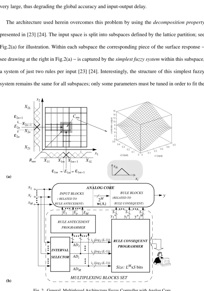
II. MIXED-SIGNAL HIGH-COMPLEXITY FUZZY CONTROLLER ARCHITECTURE
The proposed controller is based on a zero-order Takagi-Sugeno fuzzy system whose rules,
have singletons in the consequents. The surface response is interpolated from the singletons as
(1)
where the multi-dimensional basis functions are evaluated by extracting the minimum from the values of the one-dimensional membership functions associated to the k-th rule,
and are chosen to generate a lattice partition of the input space [19] [20] − see Fig.2(a) for illustration of lattice partitions.
This type of inference with lattice partitions has been employed in different implementations. Its advantages are simplicity, generality and ease of programmability [21] [22]. As a counterpart, the number of rules needed to perform a good approximation becomes prohibitively large as the number of inputs increases [20]. Since in fully-analog implementations the errors and parasitic
IF (x1 is A1k) AND (x2 is A2k) AND…(xM is AMk) THEN y = yk* (1≤ ≤k N)
y f x( ) yk* wk( )x
wk( )x
k=
∑
1,N ---k=∑
1,Nyk*wk*( )x
k=
∑
1,N= = =
wk( )x
sik( )xi
wk( )x = min s{ 1k( )x1 ,s2k( )x2 , ,... sMk( )xM }
capacitances at the global computation nodes grow with the number of rules, these errors become very large, thus degrading the global accuracy and input-output delay.
The architecture used herein overcomes this problem by using the decomposition property
presented in [23] [24]. The input space is split into subspaces defined by the lattice partition; see Fig.2(a) for illustration. Within each subspace the corresponding piece of the surface response − see drawing at the right in Fig.2(a) − is captured by the simplest fuzzy system within this subspace, a system of just two rules per input [23] [24]. Interestingly, the structure of this simplest fuzzy system remains the same for all subspaces; only some parameters must be tuned in order to fit the
Fig. 2. General Multiplexed Architecture Fuzzy Controller with Analog Core E1 Ep EM
(RELATED TO
RULE CONSEQUENT) RULE ANTECEDENT)
ANALOG CORE
RULE ANTECEDENT
Size: LMxS bits
x1
y
w(A)
S S S
2M
is (log2 (L-1)) is(log2 (L-1))
is (log2 (L-1))
INPUT BLOCKS
( RELATED TO
RULE BLOCKS
xi
xM
y1* yl* y*2M
PROGRAMMER
INTERVAL
SELECTOR
RULE CONSEQUENT
PROGRAMMER
AD1
ADi
ADM
MULTIPLEXING BLOCKS SET X11 X1m X1m+1 X1L
X21 X2L
x2
x1 Cmn
E1m E2n
ε1m ε1m+1
ε2n ε2n+1
X2n+1 X2n
Rmn
xi sik
(a)
surface response within each subspace. Thus, the strategy adopted here consists of: a) implementing a programmable analog fuzzy core for the simplest fuzzy system; b) locating the subspace corresponding to the applied inputs; c) mapping the actual subspace location onto a set of corresponding programming signals for the analog fuzzy core. Outputs are then computed by the analog core driven by the inputs and the subspace programming signals. Since errors and input-output delay are basically determined by the simple analog core, they can be kept bounded even in very complex controllers.
From now on, the generic subspace, labelled Cmn in Fig.2(a), will be called interpolation interval. Fig.2(b) shows the proposed fuzzy controller architecture for a case with inputs, labels per input − thus rules −, and where digital words of -bits per singleton are used to represent the singleton values. Two parts are clearly identified. The Analog Core at the top implements the simplest fuzzy system. The Multiplexing Blocks Set delivers the programming signals corresponding to the interpolation interval to which the actual inputs belong.
In the Multiplexing Blocks Set, a battery of simple and fast AD converters − just three bits if seven labels per input are considered − is used to codify the interpolation intervals. The digital word of 1 bits provided by these converters drives the Rule Antecedent Programmer, which provides a set of analog programming values,
, (2) and the Rule Consequent Programmer, which provides a set of digital programming values,
. (3)
These are used to program the antecedent and the consequent blocks of the Analog Core, respectively.
1. means the next superior integer of .
M L
LM S
AD1…ADM M i
s[log2(L–1)]
×
is( )x x
PACk1…kM = {E1, , , ,… Ep … EM}
PCCk
1…kM y1
* …
yl* … y
2M *
, , , ,
This system operates in asynchronous and continuous-time mode, so that its input/output delay is bounded only by the intrinsic circuit response time. In order to preserve the analog performance, the multiplexing blocks must be designed to minimize their effects on global parameters, such as the input/output delay, errors, etc. In the following, we will describe the implementation of the blocks in Fig.2(b). This description includes considerations pertaining to a general case and details pertaining to the bidimensional case implemented at the MFCON controller prototype.
III. ANALOG CORE
The analog core of Fig.2(b) implements the Takagi-Sugeno algorithm in (1) in a controller with two inputs, therefore four rules, which has a generic interpolation interval as the input space − see Fig.3(a). The circuitry is based on that previously reported by the authors in [14], although some important modifications have been made to incorporate programmability, as well as to save area and power.
ε1m ε1m+1
ε2n
ε2n+1
Fig. 3. (a) Interpolation interval and related parameters, (b) analog core architecture, (c) input block, (d) rule block
X1m+1=X1b X1m=X1a
Cmn
x2
x1 X2n+1=X2b
X2n=X2a
Rmn= R1 Rm+1n= R2 Rm+1n+1= R4
Rmn+1= R3 x1
x2
E
1,E2
( ) (y1∗,y2∗,y3∗,y4∗)
Rule Block
Rule Block
Rule Block
Rule Block
In
p
u
t
Bloc
k
In
p
u
t
Blo
c
k
yNA
Programming Interface
min
output norm weighting wl wl*
RULE BLOCK
Common NodeGl
yl∗ Xib
sia
min inp
min inp
INPUT BLOCK
Xia
xi
MFC
sib Ep
E
1
E2
R1
R2
R3
R4
X1a
X2b
X2b
X1b
X1a
X1b
X2a
X2a
(a) (b)
(c) (d)
min inp
2M-1
min inp
min inp min inp
The core is composed of instances of two main building blocks, namely the Input Block− see Fig.3(c) − and the Rule Block− see Fig.3(d). There is one Input Block per input, hence two in total; and one Rule Block per rule of the simplest fuzzy system, hence four in total. These six blocks are wired as depicted in Fig.3(b) to form the core. Programming of the input blocks is made through voltages that locate the center of the interpolation interval − see Fig.3(a). On the other hand, programming of the rule blocks is realized through digital signals which codify the singleton values.
Note that rules R1 and R3 in Fig.3(a) are rules R2 and R4, respectively, in the interval located at
left of that depicted in the figure. This means that a rearrangement of the rules is required when there is a change of the interpolation interval and the core is programmed. This rearrangement is realized by analog multiplexors in other programmable architectures [13][25]; here, however, the core architecture is fixed, and the rearrangement is realized by digital multiplexors in the programming interface − details are found in Section IV.E. On the one hand, this strategy is much more robust; on the other, it yields a significant reduction of errors, delays and interferences.
A. Input Block Circuitry
As Fig.3(c) shows, the input block accepts two types of inputs, the set of controller inputs and the set of programming signals ; and delivers two sets of outputs. Fig.4(b) shows the schematics of the input block. The front-end differential amplifier is employed to obtain the membership functions associated to labels and (see Fig.3(a)). Hence, programmability of the central point location is readily implemented by driving the differential pair with the voltage . Also, since these membership functions are complementary, a simple differential pair suffices to provide both, as Fig.4(a) illustrates. This is exploited to simplify the implementation of the minimum operator by using De Morgan’s Law, i.e. with complement plus maximum circuits.
Note in Fig.4(b) that the differential pair outputs are replicated by current mirrors and then used
xi
Ep 2M–1
Xia Xib
to drive the so-called input cells of the minimum circuit [26]. The output cell of this circuit is implemented in the Rule Block − see Fig.3(d). For a given set of currents associated to corresponding minimum circuit input cells, the maximum among them is selected by wiring the output nodes of these cells, see Fig.4(b), to the node of Fig.3(d).
Table 1 gives some expressions related to circuit design and performance.
in Table 1 is the large signal gain transconductance factor of the Mi transistor in Fig.4(b) and and are the NMOS and PMOS transistor threshold voltages, respectively. Note that the Input Block constitutes the global input interface, thus its input range is also the controller input range.
IQ sib sia sia sib
xi Ep,0
gm
Ep xi
VQB VQT Vp
VGib1 VGib2 VGia1
VGia2
minimum circuit input cell "min-inp"
membership function circuit core
(b) (a)
Fig. 4. (a) Differential pair, (b) Input Block schematic Mi MEB MET
MQB
MQT
Vp
Mpolp
Ipolp
VQB VQT
Ipoln IQ
Mpoln
s
ib
I
Q
2
⁄
+
IQ⁄2
IQ⁄2
IQ sib
sia
sia sib
MMba MMta
MMbb MMtb
Ep
xi Mi P
Mi (W/L) MET (W/L) MEB (W/L) MQT (W/L) MQB (W/L) MMta,b (W/L)
21.6µm/12µm 24µm/4µm 24µm/0.8µm 12µm/0.8µm 12µm/6µm 9µm/4.2µm
MMba,b (W/L) Mpoln (W/L) Mpolp (W/L) Ipolp Ipoln IQ
9µm/4.2µm 5µm/20µm 5µm/18µm 5µA 5µA 20µA
Input Block output nodes
Input Block output nodes
Gl
Table 1: Main design equations for the Input Block
Input range
Membership function shape
Power consumption , in Fig.4
VQT+ IQ⁄(2βi)≤ ≤xi Vp+VT0n+VT0p
sib( )xi = IQ⁄2+ IQβi⁄2(xi–Ep) 1–(xi–Ep)2βi⁄2IQ , xi–Ep ≤xˆ Pinput_block 2IQ 2
2M–1 1 +
( )VDD
= M(number of inputs) = 2
βi = β0⋅(Wi⁄Li)
VT0n
Voltages and are generated to keep MET and MEB in the top mirror, as well as MQT and MQ B i n t h e b o t t o m m i r r o r, i n t h e s a t u r a t i o n r e g i o n , w h i c h m e a n s
a n d . T h e s e
voltages are obtained from the bias circuits in Fig.4(b). The parameter is chosen to obtain the desired smoothness, which improves for smaller values of −see Fig.5. A bias current is added to the differential pair output in Fig.4(b) to prevent the transistors at the top mirror from entering in weak inversion, which would degrade the dynamic response.
B. Rule Block and Output
Fig.3(d) shows the operators within the generic high level Rule Block, while Fig.6 shows its CMOS implementation in the MFCON chip prototype, and Table 2 its main design equations. First, as already said above, the minimum circuit output cell provides the rule antecedent output in Fig.6, where is needed to perform the complement at output required by De Morgan’s law and provides a path to discharge node . Thus, the normalization is performed in every rule block by the normalization circuit unit cell in Fig.6 [14] to obtain . The bias current source and the sink transistor are shared by all rule blocks in the analog core. Every normalization circuit output is reflected by a PMOS current mirror and weighted by the singleton value − represented by the binary code in Fig.6; also the current offset is added to improve the dynamic performance. This weighting is carried out by a digitally programmable current mirror. However,
Vp VQT
Vp≤VDD–(VT0p+ IQ⁄βET+ IQ⁄βEB) VQT≥VT0n+ IQ⁄βQB+ IQ⁄βQT
xˆ ≤ IQ⁄βi xˆ
IQ⁄2
xi IQ
Ep,0
gm
Ep+ IQ⁄βi Ep– IQ⁄βi
Ep–xˆ Ep+xˆ
Fig. 5. Membership function support
sib sia
sia sib
wl
IC
Ib Gl
wl* ISS
MA
y*l
the dynamical programming of the mirror can cause large current spikes at output unless a special design is made. This design introduces the top branches at Fig.6 that are controlled by , thus they drive some current when their associated switch in the output branch governed by is ON, and vice versa. This guarantees that transistors in the current mirror are always in the saturation region, and never in the ohmic region. Since transitions from the ohmic to the saturation region were found to be the cause of the large spikes at output, the latter are reduced drastically with the proposed design.
Since the singleton weighting circuit provides a current as output, and the final processing step of the algorithm is the addition of these currents, we just wire up the rule block outputs, as Fig.3(b)
Table 2: Main design equations for the Rule Block.
Rule anteced-ent out-put Normal-ization circuit output Power Maxi-mum output rules error contribu-tion Mini-mum output rules error contribu-tion
wl=IC–IQ⁄2–max s{ 1l( )x1 ,s2l( )x2 , ,... sMl( )xM } = min s{ 1l( )x1 ,s2l( )x2 , ,... sMl( )xM }
=
wl* βtl
βbl
---wl 1 η( )w
wl
---+ 2
= η( )w
wl
l
∑
2M --- 1
Nβbl
βtl
---ISS wl
l
∑
– wl l∑
2---+ –1
=
Ib+IC+(y∗+2)Ioff
[ ]VDD≤ ≤P [Ib+IC+(y∗+2)(Ioff+ISS)]VDD
σ2
yI ss
( ) ISS2 σ
2 β SB
( )
βSB 2
--- ISS4βSBσ2(VTSB) 2Ioff2 σ
2 β OB
( )
βOB 2
---+Ioff8βOBσ2(VTOB)+ +
+ =
2(Ioff+ISS)2σ
2 β PS
( )
βPS 2
--- 8(Ioff+ISS)βPSσ2(VTPS) 2(Ioff+ISS)2σ
2 β YB ( ) βYB 2 ---+ + + + 8
+ (Ioff+ISS)βYBσ2(VTYB) +2Ioff2 σ
2
βPY
( )
βPY 2
---+8IoffβPYσ2(VTPY)
σ2
y0
( ) 2(y∗Ioff)
2 σ 2 β OB ( ) βOB 2
--- 4βSB
Ioff
---σ2(VTOB)
+ 2(y∗Ioff)
2 σ 2 β PS ( ) βPS 2
--- 4βPS
Ioff
---σ2(VTPS) + + + = 1 1 y∗ ---+
y∗I
off
( )2 σ
2
βYB
( )
βYB 2
--- 4βYB
Ioff
---σ2(VTYB)
+ 1 1
y∗
---+
y∗I
off
( )2 σ
2
βPY
( )
βPY 2
--- 4βPY
Ioff
---σ2(VTPY)
+
+ +
dl0,…l3
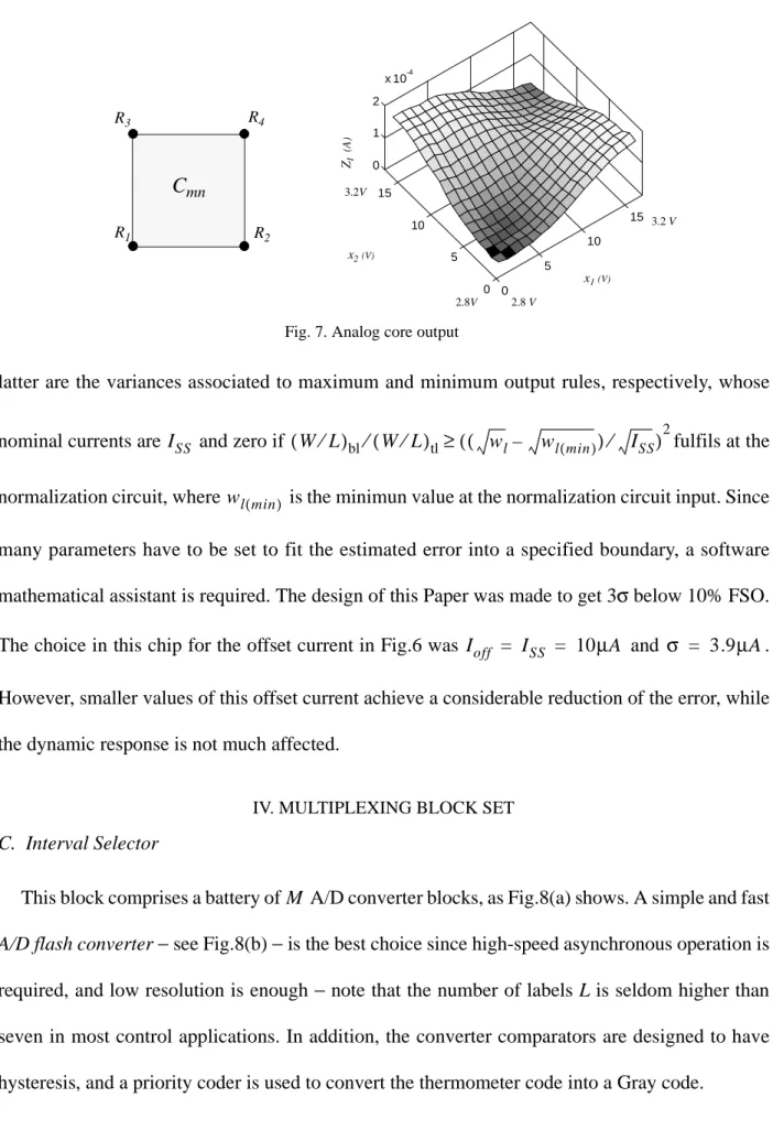
illustrates, to exploit KCL and obtain a current which enters the global output node. However, we still reflect this output current with a current mirror to get a current that leaves the controller.The output current range is , thus 150µA FSO (Full Scale Output) for the chip of this Paper. Fig.7 shows the output of the analog core for an interpolation interval of MFCON as measured in the laboratory.
With respect to errors, note first that those of systematic nature are minimized by using symmetrical structures and cascode transistors. Hence, most important errors are of random nature, due to transistor mismatches. The boundary at a given fuzzy set core [20] or interpolation point is
determined by , where and are found in Table 2. The
Mo (W/L) MC (W/L) Mbl (W/L) Mtl (W/L) MPSC(W/L) MPS (W/L) MA (W/L) MYB (W/L) MYT (W/L)
9µm/4.4µm 9µm/0.8µm 13µm/5µm 5µm/13µm 25µm/0.8µm 25µm/4µm 40µm/10µm 10µm/4µm 10µm/0.8µm ISS Ioff MPpolIc(W/L) IpolIc MPTIc(W/L) MPBIc(W/L) IC MPpolMc(W/L) IpolMc
10µA 10µA 5µm/18µm 5µA 16µm/10µm 16µm/0.8µm 30µA 10µm/8µm 5µA
MIb(W/L) Ib MPY(W/L) MPYC(W/L) MST(W/L) MSB(W/L) MOT(W/L) MOB(W/L)
1.2µm/13.6µm 0.5µA 20µm/4µm 20µm/0.8µm 20µm/0.8µm 20µm/4µm 12µm/0.8µm 12µm/6µm
dl0 dl1 dl3 VpolMc
VGl
Anor Bnor
yl dl0 dl1 dl3
1 1 2 8
normalization circuit unit cell
singleton weighting circuitry minimum circuit output cell
Fig. 6. Rule Block schematic
Ib IC
Msink
Ioff
Ioff
Ioff Ioff
ISS IC
Ib
Ib IC
VpolMc
MPpolMc
IpolMc
VSB VST
ISS ISS Ioff
Ioff
MPS
MPSC
MA
Mbl
MO MC
MSB MST
MPY MPYC MYB
MYT
Ioff
MOB MOT VpolIc
MPTIc
MPBIc
Ol
MPpolIc
IpolIc
MIb
dl2
dl2 Ioff
4
wl
wl* Mtl
0 , ISS×(2S–1)
[ ]
σ2 y
( ) σ2
yI
ss
( )+3σ2( )y0
= σ2 yI
ss
( ) σ2
latter are the variances associated to maximum and minimum output rules, respectively, whose
nominal currents are and zero if fulfils at the
normalization circuit, where is the minimun value at the normalization circuit input. Since many parameters have to be set to fit the estimated error into a specified boundary, a software mathematical assistant is required. The design of this Paper was made to get 3σ below 10% FSO.
The choice in this chip for the offset current in Fig.6was and . However, smaller values of this offset current achieve a considerable reduction of the error, while
the dynamic response is not much affected.
IV. MULTIPLEXING BLOCK SET
C. Interval Selector
This block comprises a battery of A/D converter blocks, as Fig.8(a) shows. A simple and fast
A/D flash converter− see Fig.8(b) − is the best choice since high-speed asynchronous operation is required, and low resolution is enough − note that thenumber of labels L is seldom higher than seven in most control applications. In addition, the converter comparators are designed to have hysteresis, and a priority coder is used to convert the thermometer code into a Gray code.
0 5
10 15
0 5 10 15 0 1 2
x 10-4
ZI
(A
)
x1(V)
x2(V)
2.8V
3.2V
2.8 V
3.2 V
Cmn
R1 R2
R4 R3
Fig. 7. Analog core output
ISS (W L⁄ )bl⁄(W L⁄ )tl≥(( wl– wl min( ))⁄ ISS)2 wl min( )
Ioff = ISS = 10µA σ = 3.9µA
It is important to note that these converters are not in the signal path, but in the control path; also, they do not encode the input signal to be digitally processed, but just cluster the input space into regions. Therefore, the proposed fast flash A/D converters can readily accomplish the resolution requirements, and the input-output delay of the overall controller is hardly affected by the programming circuitry around the analog core which processes the input signal. Specifically, the estimated delay for this block in the controller presented in this Paper is 60 ns, for an input overdrive of 50mV from the reference voltage. This delay is around 10% of the measured global controller input-output delay.
There are three basic elements which make up the Interval Selector block in Fig.8(b): an array of linear resistors, a Gray encoder and an analog comparator with hysteresis. The arrays of linear resistors in the converters provide the reference values in Fig.8(b), which determine the interpolation interval bounds. In addition, they also generate the whole set of programming values
− see Fig.8(b) and Fig.3(b). Note that, if the partition is the same for all input dimensions, only one resistor array may be shared by the converters as long as the comparators have high impedance inputs, which saves area and power consumption. A conventional, serpentine-shaped polysilicon strip has been used to implement this element, while the Gray encoder has been designed with
A/D
A/D
AD1[0 : p]
A/D
x1
xi
xM
p = is [log2 (L-1)]−1 ADM[0 : p] ADi[0 : p]
Fig. 8. Interval selector building blocks: (a) battery of converters, (b) A/D flash converter structure
(a) (b)
+ −
ADi 0 ADi p
bR R R
R R R R
R R aR
εiL-1
εij+1
Eij
εij
Ei1
εi1
EiL-1
GR
A
Y
C
O
D
.
+ −
+ −
Eij+1
xi
Di1 Dij+1 DiL-1
εij
CMOS logic gates of minimum size.
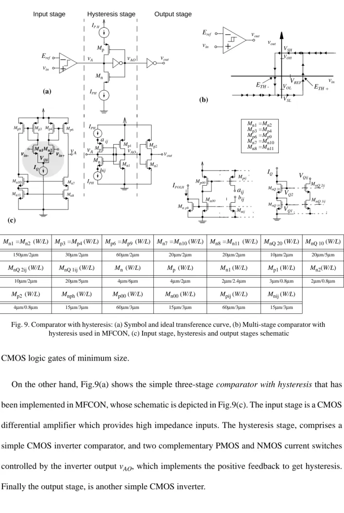
On the other hand, Fig.9(a) shows the simple three-stage comparator with hysteresis that has been implemented in MFCON, whose schematic is depicted in Fig.9(c). The input stage is a CMOS differential amplifier which provides high impedance inputs. The hysteresis stage, comprises a simple CMOS inverter comparator, and two complementary PMOS and NMOS current switches controlled by the inverter output vAO, which implements the positive feedback to get hysteresis. Finally the output stage, is another simple CMOS inverter.
+
−
+
−
Eref
vin
vout
Eref v vout
A
Mp
Mn
IP H
IPH
(b) (a)
vAO
Fig. 9. Comparator with hysteresis: (a) Symbol and ideal transference curve, (b) Multi-stage comparator with hysteresis used in MFCON, (c) Input stage, hysteresis and output stages schematic
Input stage Hysteresis stage Output stage
vin- vin+ vA
Mn1Mn2
Mp3 Mp4 Mp6
Mn7
Mn8
Mp9
Mn10 Mn11
IQ
VQij
Mn1 =Mn2 Mp3 =Mp4
Mp6 =Mp9
Mn7 =Mn10 Mn8 =Mn11
VQ2
VQ1
IQ
VQij
MnQ 20
MnQ 10
MnQ 2ij
MnQ 1ij
IPH
IPH
vAMp
Mn
Mp1 Mp2
Mn1 Mn2
aij
bij
(c)
vAO
vin
vout
VREF
ETH + ETH
-VSH
VSL
VOL VOH
IPOLH
aij
bij
Mnij
Mn00
Mn ph
Mpij
Mp00
Mn1 =Mn2 (W/L) Mp3 =Mp4 (W/L) Mp6 =Mp9 (W/L) Mn7 =Mn10(W/L) Mn8 =Mn11 (W/L) MnQ 20(W/L) MnQ 10 (W/L)
150µm/2µm 30µm/2µm 60µm/2µm 20µm/2µm 20µm/2µm 10µm/2µm 20µm/5µm
MnQ 2ij(W/L) MnQ 1ij (W/L) Mn (W/L) Mp (W/L) Mn1 (W/L) Mp1(W/L) Mn2(W/L)
10µm/2µm 20µm/5µm 4µm/6µm 4µm/2µm 2µm/2.4µm 3µm/0.8µm 2µm/0.8µm
Mp2 (W/L) Mnph(W/L) Mp00 (W/L) Mn00(W/L) Mpij(W/L) Mnij (W/L)
4µm/0.8µm 15µm/3µm 60µm/3µm 15µm/3µm 60µm/3µm 15µm/3µm vout
The switches in the second stage allow us to either connect or disconnect the current sources
IPH to the input inverter node vA; this either adds or substracts current at this node, thereby forcing the reference voltage of the comparator to be either or , respectively (see Fig.9(b). First-order calculations obtains,
, (4)
where gm is the small-signal transconductance of the differential stage; and , if
and , where are the output resistances of the
circuitry which implements the current sources IPH − see right part of Fig.9(c), and are the ON resistances of the NMOS and PMOS switches, respectively. The expression above shows that the hysteresis can be controlled by the current source IPH, which is derived from an external bias current IPOLH.
The Table in Fig.9 shows the sizes of the transistors in Fig.9(c) as used in MFCON. They have been designed to cope with the requirements of gain, common mode range, power consumption and errors, from the simulations and analytical expressions reported in [27].
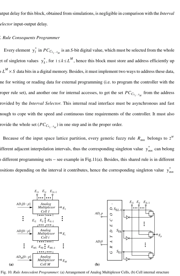
D. Rule Antecedent Programmer
The main requirements for this block are high-speed operation, as well as design simplicity, reliability and compactness. Because every element in must be selected from the whole set of programming values in Fig.8(b), this block comprises a battery of digitally controlled analog multiplexor cells, as Fig.10(a) shows. Fig.10(b) shows the internal structure of an analog multiplexor cell, which is composed of analog switches (CMOS transmission gates), and a Gray decoder which provides the digital control signals for the switches. Both elements are well-known CMOS building blocks and their design will not be explained here. The estimated
input-ETH+ ETH–
ETH+ IPHn gm
---= ETH– IPHp
gm
---– =
IPHn≈IPHp≈IPH
ronPH rDSn
ON
» ropPH rDSp
ON
» ronPH and ropPH
rDSn
ONand rDSpON
Ep PACk
1…kM
output delay for this block, obtained from simulations, is negligible in comparison with the Interval Selector input-output delay.
E. Rule Consequents Programmer
Every element in is an S-bit digital value, which must be selected from the whole set of singleton values , for , hence this block must store and address efficiently up to data bits in a digital memory. Besides, it must implement two ways to address these data, one for writing or reading data for external programming (i.e. to program the controller with the proper rule set), and another one for internal accesses, to get the set from the address provided by the Interval Selector. This internal read interface must be asynchronous and fast enough to cope with the speed and continuous time requirements of the controller. It must also provide the whole set ( ) in one step and in the proper order.
Because of the input space lattice partition, every generic fuzzy rule belongs to different adjacent interpolation intervals, thus the corresponding singleton value can belong to different programming sets − see example in Fig.11(a). Besides, this shared rule is in different positions depending on the interval it contributes, hence the corresponding singleton value
Analog
AD1[0 : p]
ADM[0 : p]
ADi[0 : p]
Cell i
Cell M
E1
Ei
EM E11 E1j E1L-1
EM1 EMj EML-1 Ei1 Eij EiL-1
Cell 1 Multiplexor
Analog Multiplexor
Analog Multiplexor
Fig. 10. Rule Antecedent Programmer: (a) Arrangement of Analog Multiplexor Cells, (b) Cell internal structure
(a) (b)
Ep SEL-1
SE1 SEk
GR
A
Y
D
E
C
O
D
. Ei1 Eij EiL-1
ADi0 ADi p yl* PCCk
1…kM
yk* 1≤ ≤k LM LM×S
PCCk1…kM
PCCk1…kM
Rmn 2M
ymn*
must appear in different locations in the programming bus − see Fig.11(b), because this bus is fixed in the Analog Core side as discussed in Section III.
The design of this block is based on the generic conceptual architecture for internal accesses depicted in Fig.12(a). The figure shows how the data are distributed into different blocks of
Memory Cells, which contain subsets of singleton values which will never be addressed simultaneously. For a given address, the Row Selector selects one row per Memory Cell block simultaneously, thus all needed singleton values are ready to be accessed. At the same time, the
Cmn
C(m-1)(n-1)Cm(n-1) C(m-1)n
Rmn
ε1m ε1m+1
ε1m-1
ε2n ε2n+1
ε2n-1
(a)
(b)
Fig. 11. (a) Rmn is active rule in four adjacent intervals: , (b) Rule order and programming bus example for two adjacent intervals
Cmn,Cm n( –1),C(m–1)n,C(m–1)(n–1)
( )
y*mn y*(m+1)n
y*m(n+1) y*(m+1)(n+1)
y*(m-1)n y*(m-1)(n+1)
C(m-1)n Cmn C(m-1)n
1 2
3 4
Cmn
1 2
3 4
y*mn y*(m+1)n y*m(n+1) y*(m+1)(n+1)
y*(m-1)n y*mn y*(m-1)(n+1) y*m(n+1)
PCCmn={
PCC(m-1)n={
}
}
R(m-1)n Rmn
Rm(n+1) R
(m+1)(n+1)
R(m-1)(n+1)
Rmn Rm(n+1)
R(m+1)n
1 2 3 4
Fig. 12. (a) Rule Consequents Programmer conceptual internal architecture, (b) Internal accesses interface timing 2M -1
LM
2M -1xS bits
Memory Cells
Column
Selector Row Selector M x is (log2 (L-1))
LM -1 2M -1 2M -1
LM -1
2M -1
LxS Lx S
2MxS MUX
(2M -1xL) x1
2MxS bits
(M-1) + is(log2 (L-1))
block
LM
2M -1xS bits
Memory Cells block
(M-1) x is (log2 (L-1))
tdad
twa
ADR
DAT
ADRa ADRb ADRc ADRd
DATa DATb DATc DATd
(a) (b)
ADR
Column Selector controls the multiplexor to locate properly every singleton value in the programming bus. Fig.12(b) illustrates the timing of these accesses.
Fig.13 illustrates the organization and interfaces of the building blocks in the CMOS implementation of the Rule Consequent Programmer in MFCON based on Fig.12(a). These blocks are Memory Cells, Row Selector, Column Selector for Internal Accesses and Column Selector for External Accesses.
The basic building block of the Memory Cell blocks in MFCON is shown in Fig.14(a). It comprises four one-bit memory basic cells, associated to two different Memory Cell Blocks in Fig.12(a). Specifically, row n in Fig.14(a) comprises one-bit basic memory cells (m,n) and
(m+1,n), which belong to the Memory Cell Block 2, while row n+1 comprises the cells (m,n+1)
Memory Cell blocks
Basic Building
Block
Row
Selector Basic Select.
MUX 8 X1
MUX 16 X1 MUX 16 X1 MUX 16 X1 MUX 16 X1
Exter. Rd. Dat. Exter. Wr. Dat.
Intr.Rd.Dat1 Intr.Rd.Dat.2.
Column Selector
Column Selector
Internal
Addressing Accesses External
Addressing Accesses
Data Interface for external accesses
Data Interface for internal accesses Wiring
For External Accesses
For Internal Accesses
Fig. 13. Organization of the different building blocks used in the CMOS implementation of the Rule Consequent Programmer in MFCON.
Intr.Rd.Dat3 Intr.Rd.Dat.4. Control
and (m+1,n+1) which belong to the Memory Cell Block 1. For internal read accesses, switches sm
and sm+1 are open, thus memory cells (m,n) and (m+1,n) are in different column lines in the
Memory Cell Block 2, while (m,n+1) and (m+1,n+1) are in different column lines in the Memory Cell Block 1. Therefore, the four stored bits can be read simultaneously if both row lines are selected for internal accesses. However, for external accesses, switches sm and sm+1 are closed, so memory cells (m,n) and (m+1,n) belong to the same column line, as well as (m,n+1) and
(m+1,n+1). Thus, the whole block is configured to be accessed as a two-row, two-column conventional memory block, and the memory is a conventional RAM for external accesses. Fig.14(b) shows the elements in one column of the basic building block in Fig.14(a). The one-bit basic memory cell used in MFCON (enclosed in dash square in Fig.14(b)), is a single-ended bit-line static CMOS cell [28], which is common in register files and multiport memories. Because of the flexibility in changing its configuration, and its robustness [29], this cell results very suitable for the reconfiguration requirements of this application. Fig.14(b) also shows the switches for reconfiguration and the latches for regenerating the logic levels. The transistor sizes in the memory
(m,n) (m+1,n)
(m,n+1) (m+1,n+1) Wr.Dat.
Col.m
WR.Dat. Col.m+1
RD.Dat.
Col.m sm RDCol. .Dat.m+1 sm+1
WR.Sel. Row n
WR.Sel. Row n+1
RD.Sel. Row n
RD.Sel. Row n+1
RD.Dat.Col.m Cell Block 2
RD.Dat.Col.m+1 Cell Block 2 RD.Dat.Col.m
Cell Block 1 Cell Block 1RD.Dat.Col.m+1
Data Interface for external accesses
Data Interface for internal accesses
Ro
w
Sel
ecti
o
n
I
n
terface
Sel_RWRn Sel_RRDn Ext.
N1 N2
INV1
INV2 INV3
Sel_RWRn+1 Sel_RRDn+1 WR.Dat.
RD.Ext.Dat.
N1 N2
INV1
INV2 INV3
INV4
INV5
INV6
INV7 INV6
INV7
sm
swc Sel_CWRn
Col m
RD.Dat.Col.m CellBlock2
RD.Dat.Col.m CellBlock1 Ext. sw2m sw1m
(m,n)
(m,n+1)
Fig. 14. (a) Memory Cell basic building block, (b) Detail of the elements of one column: Basic Memory Cell (enclosed in dashed square), reconfiguration switches and column sensed latches
cell have been determined from the design recommendations in [28].
The Row Selector activates the proper row selection lines after decoding the access type (read/ write) and origin (internal/external) and the corresponding subset of address lines − see Fig.13. For external accesses the block works as a conventional binary decoder, while for internal accesses it works as a Gray decoder which activates simultaneously several row selection lines per access, one per Memory Cell block considered. Fig.15(a) illustrates the conceptual architecture and interfaces, while Fig.15(b) illustrates the basic building block of the Row Selector as implemented in MFCON.
Because internal accesses are always for reading, the Column Selector for Internal Accesses
comprises a battery of properly sized multiplexors with shared control lines, as Fig.15(c) illustrates, where the conceptual architecture and interfaces of this block in MFCON are shown. Because column data lines are properly wired to the multiplexor inputs, the control block can be
Dec Bin 3:8 0 1 2 3 4 5 6 7 D2 D1 D0 Ena Sel_FWR1 Sel_FRD1 Sel_FWR2 Sel_FRD2 Sel_FWR3 Sel_FRD3 Sel_FWR4 Sel_FRD4 Sel_FWR5 Sel_FRD5 Sel_FWR6 Sel_FRD6 Sel_FWR7 Sel_FRD7 Sel_FWR8 Sel_FRD8 Sele_F1 Sele_F2 Sele_F3 Sele_F5 Sele_F5 Sele_F6 Sele_F7 Sele_F8 Dec Gray 0 1 2 3 4 5 6 7 D2 D1 D0 Ena Seli_F1 Seli_F2 Seli_F3 Seli_F5 Seli_F5 Seli_F6 Seli_F7 Seli_F8 MUX_SEL WR_RD Ext External Address Internal Address AExt[2:0] AInt[2:0] 3 2 Row Selector Basic Building Cell AD Bits Ext. AD Bitsr Int.
ExtExt WR_RD WR_RD Sel_FWRi Sel_FRDi Ext Ext WR_RD WR_RD Ext Ext WR_RD WR_RD Sel_FWRi Sel_FRDi AD Bit Ext. AD Bit Int.
Col.1 Col.2 Col.3 Col.4 Col.5 Col.6 Col.7 Col.8 Col.9 Col.10 Col.11 Col.12 Col.13 Col.14 Col.15 Col.16
4 y* mn MUX1 16x1 4 y* m+1n+1 MUX4 16x1 4 y* mn+1 MUX3 16x1 4 y* m+1n MUX2 16x1
4 C 4 4 4
C C C
WIRING
Memory Cell blocks Interface
Analog Core Interface
4 C Column Selection Control 3 3 ADm ADn Mem
ory Cell blo
ck s in terf ace In terval S e lecto r In te rf a c e
Fig. 15. (a) Row Selector conceptual architecture, and (b) Basic building block, (c) Column Selector for Internal Accesses conceptual architecture
(a) (b)
very simple.
The Column Selector for External Accesses comprises a control block and a multiplexor per output line − see Fig.13. The control block contains a decoder which activates the proper column selection lines by decoding a subset of the corresponding address lines for write accesses. On the other hand, the multiplexors are controlled by the same subset of address lines to provide the data in read accesses.
V. STATIC AND DYNAMIC PERFORMANCES OF MFCON
The MFCON controller prototype has been integrated in a single-poly, double-metal CMOS 0.7µm technology offered in EUROPRACTICE. The chip was simulated with HSPICE and designed with Design Frame Work II. It implements the architecture of Fig.2 with two inputs ( ), eight labels per input ( ),and four bits per singleton ( ). Fig.16(a) shows a microphotograph of the chip, and Fig.16(b) shows the floorplan of the chip with the blocks and their sizes. Conservative layout strategies have been adopted; particularly, the analog circuitry has been placed far away from the digital one, with large isolation guard rings in between 1. Also, in order to further reduce interferences between these parts, separate pins and lines have been employed for the analog supply, the digital supply, and the ground [30].
1. The area occupation of this chips, around 5mm2, is much larger than needed. Since 5mm2 is the minimum area for MPW projects, largely conservative layout floorplanning strategies have been adopted regarding the separation of analog and digital parts.
M = 2 L = 8 S = 4
Fig. 16. (a) Microphotography and (b) Floor plan of the chip PADS area
MEMORY
A/D_C
W_SEL ANALOGCORE VO
0.84 mm2
0.30 mm2 0.27 mm2
0.02
Rings Guard
mm2
Fig.17(a) shows the chip pin-out, while Fig.17(b) shows the digital and analog interfaces with the pins grouped in buses. On the one hand, the digital interface corresponds to a typical asynchronous peripheral for microcontroller-based systems, with an input address bus (A{0:5}), a bidirectional data bus (D{0:3}) and a control bus (COM, W-R). On the other hand, the analog interface is composed of the controller input and output signals, and a few off-chip bias signals to simplify testing of the prototype. These signals should be generated on-chip in a marketable final version.
The fuzzy controller inputs are and , which are driven by voltage mode signals in the range from 2.0V to 4.8 V. The primary fuzzy controller output is − a current signal in the range from 0µA to 150µA. A voltage output is also provided at . This voltage is obtained by applying a replica of to an on-chip polysilicon resistor. Every singleton value is a four-bit digital word which encodes sixteen uniformly distributed analog values in the output current range.
Fig.18 and Fig.19 show some experimental results obtained from the test environment. Fig.18(a) depicts a section of a measured DC control surface, and Fig.18(b) shows the transient response to a step input. The former illustrates the response (bottom) to a ramp in one input (top) while the other input remains constant, in a kind of mexican hat surface. The latter corresponds to
Fig. 17. Fuzzy controller chip: (a) pin-out; (b) interfaces
A(0:5) D(0:3)
COM,W-R
IPs,VREF Digital
Analog
FUZZY CHIP CONTROLLER ADDRESS DATA
CONTROL
OUTPUTS INPUTS
BIAS Interface
Interface
x1,x2 zI,zV 1
2 3 4 5 6 7 8 9 10 11 12 13
14 15
16 17 18 19 20 21 22 23 24 25 26 27 28 A1
A0 GNDG VREF IPH VDDA X1 X2 IPN IPG IPV GNDA ZV
ZI GNDG
A5 A4 A3 GNDD D3 D2 COM D1 D0 VDDD W_R A2
(a)
(b)
x1 x2
zI
zV
a falling edge in one input which forces the output to change from its maximum to its minimum value, as well as to jump to a different interpolation interval, which means a dynamic programming of the analog core. The measured delay time is around 500ns. Since the oscilloscope is not able to sense currents, previous measurements are voltages in the output . With regard to Fig.19(b) and Fig.19(d), they are built with data obtained from a data acquisition board, where the current output
x1 (V) zV (V ) time x1 (V) zV (V ) time
x2 =3.2 V x2 =3.2 V
Fig. 18. Measured results: (a) DC nonlinear control surface section, (b) transient falling edge step response.
(a) (b)
(a) (b)
Fig. 19. Control surface measured results: (a) programming rule matrix I, (b) nonlinear control surface I, (c) programing rule matrix II and (d) nonlinear control surface II
(c) (d)
2.0V
4.8V
2.0 V
4.8 V
x1(V)
x2(V)
ZI (A ) 0 15 0 0 0 15 15 15 0 15 0 0 0 15 15 15 0 15 0 0 0 15 15 15 0 15 0 0 0 15 15 15 0 15 0 0 0 15 15 15 0 15 0 0 0 15 15 15 0 15 0 0 0 15 15 15 0 15 0 0 0 15 15 15
X11 X18
X21
X28
x2
x1 Rule Matrix
4.4 V
2.0 V 2.0 V
4.4 V
x1(V)
x2(V) ZI (A ) 0 0 10 10 0 10 10 0 10 10 0 0 10 0 0 10 0 0 10 10 0 10 10 0 10 10 0 0 10 0 0 10 5 5 14 14 5 14 14 5 14 14 5 5 14 5 5 14 5 5 14 14 5 14 14 5 14 14 5 5 14 5 5 14
X11 X18
of the chip is externally converted into a digital word and processed. Both figures illustrate the ability of the controller to interpolate functions. Finally, the measured chip power consumption was around 16mW, which is obtained by sensing the current from the supply voltage sources.
In addition, Fig.20 shows results from an example application with the chip in a control loop. The task is the start of a DC motor controlled with a PWM DC-DC switching converter at 100kHz. Fig.20(a) shows the control surface, while Fig.20(b) and Fig.20(c) show the motor speed (top) and armature current (bottom) for both, the direct start and controlled soft-start, respectively. Note that the speed rise time is similar in both, direct and controlled cases, while the initial current spike is not present in the controlled case. Fig.20(d) shows how smooth the control is in the range of microseconds. Finally, Fig.20(e) shows that the current is not got under control if the same strategy is implemented with a microcontroller.
VI. CONCLUSIONS
The mixed-signal fuzzy controller chip presented in this Paper attains the performance levels of fully analog controllers while overcoming their inherent limitations in terms of programmability and complexity. This is achieved by employing the multiplexing strategy and architecture presented by the authors in [1]. The data in Table 3 are intended to compare the MFCON chip to
Table 3: CMOS Analog implementation of Fuzzy Controllers
Features/
CMOS Chips Manaresi [12] Guo [13] Vidal [14] Baturone [15] MFCON
Complexity 9rules@2inputs
@2output
13rules@3inputs @1output
16rules@2inputs @1output
9rules@2inputs @1output
64rules@2inputs @1output
Technology 0.7µm CMOS 2.4µm CMOS 1µm CMOS 2.4µm CMOS 0.7µm CMOS
Power 44mW@5V 550mW@10V 8.6mW@5V 21mW@5V 16mW@5V
In/out Delay 570 ns 160 ns 471 ns 2000 ns 500 ns
Precision No data No data 6.5% (3σ) No data 7.8%(3σ)
Interface (in@out)
volt@volt volt@volt volt@current volt@volt volt@current
Programmability HIGH LOW HIGH HIGH HIGH
Area 1.9 mm2 16.2 mm2 1.6 mm2 1.1 mm2 2.65 mm2
other analog continuos-time CMOS controller chips which implement a similar inference algorithm.
From Table 3 it is seen that the MFCON chip implements much more rules that the others. Note also that this increased number of rules is not accompanied by a significant power consumption increase; neither by an operation speed drop. Actually, regarding power consumption, only the
2 V
4.4 V
2 V
4.4 V
VIm (V) Vω(V)
ID
(A
)
Fig. 20. Start of a DC motor control example: Control surface (a); curves for the speed Vω and armature current VIm for direct (b) and controlled (c) start; controlled start detail with MFCON (d) and controlled
start detail with microcontroller (e). (a)
VD
(
V
)
VIm
(
V
)
VIm
(V)
Vω
(V
)
VIm
(V
)
SC
(V)
controller
DC motor
D (ω, Im)
and switchig converter
(d) (e)
VIm
(V)
V
ω
(V
)
(b)
(c)
500µs 500µs
Im= 800mA
prototype in [14] consumes less power than the MFCON chip, although it realizes four times less rules. Regarding speed, the prototype in [13] is faster, although its power consumption is much larger and its complexity much smaller.
The data in Table 3 confirms that the proposed strategy actually overcomes the limitations of purely analog controllers while keeping their performance advantages. For instance, a fully analog controller designed by the authors [14] using similar circuitry yields 470ns and 8.6mW for 16 rules, while the MFCON chip yields 500ns and 16mW for 64 rules. Advantages of the proposed architecture become more evident as the number of rules and inputs increases [1]. Furthermore, the proposed architecture is very well suited for the modular generation of complex fuzzy controllers. Since it is based on the dynamical programming of an analog core, whose size − rules − depends just on the number of inputs M, we could have a reduced set of well-designed analog cores (one input, two inputs, three inputs...) as cells. Every cell is valid for building controllers with a different number of rules, while their performances must be quite similar in terms of errors, power consumption and input-output delay. These cells could even be integrated in conventional microcontrollers which would provide a very good control performance.
REFERENCES
[1] F. Vidal-Verdú, R. Navas-González and A. Rodríguez-Vázquez, "Multiplexing architecture for mixed-signal CMOS fuzzy controllers", Electronics Letters, vol.34 no.14 pp. 1437-1438, July 1998
[2] M. Brown and C. Harris, NeuroFuzzy Adaptive Modeling and Control, prentice Hall International, 1994.
[3] Werbos et al. "Neural Networks, System Identification and Control in the Chemical Process Industries", in Handbook of Intelligent Control, Eds White D. A., Van Nostrand Reinhold, NY, Chapter 10, 1992
[4] K. Hirota y M. Sugeno, Industrial Applications of Fuzzy Thechnology in the World. World Scientific. 1995.
[5] B. K. Bose, " Expert Systems, Fuzzy Logic, and Neural Network Applications in Power Electronic and Motion Control" Proceedings of the IEEE, Vol. 82, pp. 1303-1323, August 1994.
[6] K. Young-Ho and K. Lark-Kyo, "Design of Neuro-Fuzzy Controller for the Speed Control of a DC Servo Motor", Proceeding of the V International Conference on Electrical Machines and Systems, vol. 2, pp. 731-734, August 2001.
Induction Motor Drive with Space Vector PWM and Flux-Vector Synthesis by Neural Networks", IEEE Transactions on Industry Applications, vol. 37, no. 5, Sep./Oct. 2001. [8] M. Criscione, G. Giustolisi, A. Lionetto, M. Muscarà, G. Palumbo, "A Fuzzy Controller for
Step-Up DC/DC converters", The 8th. IEEE Inter. Conf. on Electronics, Circuits and Systems (ICECS 2001), vol. 2 pp.977-980, 2001.
[9] E. Franchi, N. Manaresi, R. Rovatti, A. Bellini, and G. Baccarani, "Analog Synthesis of Nonlinear Functions Based on Fuzzy Logic", IEEE Journal of Solid-State Circuits, vol. 33, no. 6, June 1998.
[10] Sanchez-Solano, S., Barriga A., Jiménez C..J., Huertas J.L. "Design and Application of Digital Fuzzy Controllers", Procc. IEEE Int. Conf. on Fuzzy Systems, pp. 869-874, Barcelona, 1997.
[11] Gabrielli, A. Gandolfi E., Masetti M., "Design of a Family of VLSI High Speed Fuzzy Processors", Procc. IEEE Conf on Fuzzy Systems, pp. 1099-1105, New Orleans, 1996. [12] N.Manaresi, R. Rovatti, E. Franchi, R. Guerrieri, and G. Baccarani, “A Silicon Compiler of
Analog Fuzzy Controllers: From Behavioral Specifications to Layout”. IEEE Trans. on Fuzzy Systems, Vol. 4, pp. 418-428, November 1996.
[13] S. Guo, L. Peters, and H. Surmann, “Design and Application of an Analog Fuzzy Logic Controller”. IEEE Trans. on Fuzzy Systems, Vol. 4, pp. 429-438, November 1996.
[14] A. Rodríguez-Vázquez, R. Navas, M. Delgado-Restituto and F. Vidal-Verdú, "A Modular Programmable CMOS Analog Fuzzy Controller Chip", IEEE Transactions on Circuits and Systems-II: Analog and Digital Signal processing, Vol. 46, No.3 pp. 251-265, March 1999. [15] I. Baturone, S. Sánchez-Solano and J.L. Huertas, "Towards the IC Implementation of
Adaptive Fuzzy Systems". IEICE Transactions on Fundamentals, Vol. E-81-A, No. 9, pp. 1877-1885, 1998.
[16] Teresa Serrano-Gotarredona, Andreas G. Andreou, and Bernabé Linares-Barranco, "A Programmable VLSI Filter Architecture for Application in Real Time Vision Processing Systems," International Journal of Neural Systems, Special Issue on New Trends in Neural Network Implementations, vol. 10, No. 3, pp. 179-190, June 2000.
[17] G. Cauwenberghs, M. A. Bayoumi, Learning on Silicon. Adaptive VLSI Neural Systems, Kluwer Academic Publishers, 1999.
[18] F. Vidal-Verdú, R. Navas-González and A. Rodríguez-Vázquez, "Circuits for on-chip Learning in Neural-Network" in Learning on Silicon. Adaptive VLSI Neural Systems, Edited byG. Cauwenberghs, M. A. Bayoumi, Chapter 9, Kluwer Academic Publishers, 1999. [19] J.S.R. Jang and C.T. Sun, “Neuro-Fuzzy Modeling and Control”. Proceedings of the IEEE,
Vol. 83, pp. 378-406, March 1995.
[20] L.X.Wang, A Course in Fuzzy Systems and Control, Prentice-Hall PTR 1997.
[21] T. Miki, T. Yamakawa, “Fuzzy Inference on an Analog Fuzzy Chip”, IEEE Micro, vol. 15, no. 4, pp. 58-66, 1995.
[22] I. Baturone, S. Sanchéz-Solano, A. Barriga and J.L. Huertas, “Implementation of CMOS Fuzzy Controllers as Mixed-Signal Integrated Circuits”, IEEE Tran. on Fuzzy Systems, vol.5, no.1,Feb.1997.
[23] X.J.Zeng and M.G.Singh, “Decomposition Property of Fuzzy Systems and Its Applications”,
IEEE Tran. on Fuzzy Systems, vol. 4, no. 2, pp. 149-165, May1996.
[24] X.J.Zeng and M.G.Singh, “Approximation Accuracy Analysis of Fuzzy Systems as Function Approximators”, IEEE Tran. on Fuzzy Systems, vol. 4, no. 1, pp. 44-63, Feb.1996.
[25] I. Baturone, A. Barriga, S. Sanchéz-Solano, and J.L. Huertas, “Mixed Signal Design of a Fully Parallel Fuzzy Processor”, Electronics Letter, vol.34, no.5, pp.437-438, March.1998 [26] F. Vidal-Verdú and A. Rodríguez-Vázquez, "Using Building Blocks to Design Analog

![Fig. 6. Rule Block schematicIbIC M sinkIoffIoffIoffIoffISSICIbIbICVpolMcMPpolMcIpolMcVSBVSTISSISS I offIoffMPSMPSCMAMblMOMCMSBMST M PYM PYCMYBMYTIoffMOBMOTVpolIcMPTIcMPBIcOlMPpolIcIpolIcMIbdl2dl2Ioff4wlwl*Mtl 0 I , SS × ( 2 S – 1 )[ ] σ 2 ( )y σ 2 y I( ss](https://thumb-us.123doks.com/thumbv2/123dok_es/6311939.779777/13.892.95.799.95.1171/fig-rule-block-schematicibic-sinkioffioffioffioffissicibibicvpolmcmppolmcipolmcvsbvstississ-offioffmpsmpscmamblmomcmsbmst-pycmybmytioffmobmotvpolicmpticmpbicolmppolicipolicmibdl-ioff.webp)