Lattice defects and boundaries in conducting carbon nanotubes
14
0
0
Texto completo
(2) PHYSICAL REVIEW B 80, 075115 共2009兲. REYES, STRUCK, AND EGGERT. . .. β 2. α. x=1. a _ 2 y=1. A. Armchair CNT. Armchair carbon nanotubes are always conducting and are defined by a chiral vector with equal indices 共N , N兲.3 As. 3. 4. 5. 6. FIG. 1. 共Color online兲 ARMCHAIR: Labels chosen for the atoms in the graphene lattice in the case of the armchair CNT. The hexagonal network is composed by two triangular sublattices which are labeled ␣ and . Within the tight-binding approximation there is a hopping amplitude t between them. The label y is in the direction along the tube axis and x indicates the bonds around the tube.. usual, the atoms can be divided into two distinct sets ␣ and , corresponding to the two sublattices of the graphene honeycomb structure. It is convenient to label each of the ␣- pairs with a set of coordinates 共x , y兲 as shown in Fig. 1. The coordinate y is along the tube and x is around the tube. The tight-binding Hamiltonian can now be written as follows: N. H = − t兺. x=1. The tight-binding band structure of an infinite graphene sheet includes a valence band and a conduction band that touch at two distinct Fermi points. When this graphite monolayer is rolled into a CNT, boundary conditions are imposed such that only a finite set of bands are allowed. As mentioned above, in some cases a subset of bands coincides with the Fermi points and the tube is metallic. The present section is devoted to show how to obtain an effective low-energy theory for conducting SWCNTs by keeping only its conduction bands. The result is a dramatically simplified description of the tubes in terms of two chain models. To be able to take advantage of these simple lattice models, we do not need to recur to the widely used linearization around the Fermi points.4,31,38,39 The procedure will be outlined for the armchair and conducting zigzag nanotubes for which the conduction bands can be easily identified and isolated once a Fourier transform around the tube is performed.. 2. . . . .. II. EFFECTIVE MODELS. .. models here capture the most relevant physical effects of defects but for quantitative details future comparison with first-principles calculations would also be useful. In particular, while our exemplary vacancy model only illustrates the first-order symmetry-breaking effect, it would also be interesting to incorporate the relaxation of the structure around defects.35 While this can, in principle, be considered within the same formalism, this extension would require additional input from independent ab initio calculations about the modified hopping parameters. Electron-electron interaction effects can also be incorporated into the simple lattice models as described in the Appendix but are ignored for the calculation of the STM patterns from defect scattering to first order. This is justified because in STM experiments the Coulomb interaction becomes short range due to screening from the substrate and the effective on-site interaction Ueff = U / N is weak for large enough N.33 It is known that interaction effects result in a characteristic amplitude modulation of the scattered density waves11–14 but appear to leave the principle wave pattern intact. Nevertheless, it should be emphasized that the models presented here, are well suited for the study of strong correlations by applying the powerful techniques available for one-dimensional systems such as bosonization36 or densitymatrix renormalization group 共DMRG兲.37 For the interested reader, all additional terms necessary to take electronelectron interactions into account in the effective models are listed in the Appendix. The paper is organized as follows: In Sec. II we show how the effective theory for the perfect CNTs is obtained. Then, in Sec. III we incorporate imperfections and caps at the tube ends. We proceed similarly in Sec. IV but now considering structural deformations in the bulk of the tube. For each case, we use the effective models to obtain electron densities in real space for states near the Fermi level. The resulting patterns are the ones expected for a typical STM experiment.9,10. +. 兺. 冋兺. 共␣†x,yx,y+1 + †x,y␣x+1,y+1兲. 册. y odd L. 共†x,y␣x,y+1. +. ␣†x,yx−1,y+1兲. y even. + 兺 ␣†x,yx,y + H.c. y=1. 共1兲 Here ␣ and  are the destruction operators in the corresponding sublattice, L is the length of the tube, and N is the number of bonds around its perimeter. Performing a partial Fourier transform in the direction x around the tube and considering that the only conducting modes are the ones corresponding to k = 0 共one for each sublattice兲,3 the following approximation holds:. ␣x,y =. 1. ␣k,ye 冑N 兺 k. ikx. ⬇. 1. 冑N ␣k=0,y,. k=. 2l , N. 共2兲. and analogously for . Since the k = 0 mode is the only one that will be taken into account, we drop the k index in the following. Performing the linear transformation. 075115-2.
(3) PHYSICAL REVIEW B 80, 075115 共2009兲. LATTICE DEFECTS AND BOUNDARIES IN CONDUCTING…. (a). t. µ. −t. −µ. S A . . .. E(ky) 3t. 4. A−band. −π. −2π 3. π. 2π 3. 3. ky. S−band. 2. (b). FIG. 2. 共a兲 Effective chain lattice model for the perfect armchair carbon nanotube. The upper chain corresponds to the symmetric 共S兲 mode and the lower one to the antisymmetric 共A兲 mode. In this case = t. 共b兲 Band structure for the conducting modes 共effective lattice spacing aeff = a / 2兲.. ␣y =. Sy + Ay. 冑2. ,. y =. Sy − Ay. 冑2. 共3兲. ,. the effective conduction-band Hamiltonian can be written in terms of two completely independent parts, each one of them involving only the symmetric 共S兲 or antisymmetric 共A兲 mode 共4兲. Heff = HS + HA . Inserting Eqs. 共2兲 and 共3兲 into Eq. 共1兲 we find HS = − t 兺 y. 冉. S†y Sy+1. 1 + S†y Sy + H.c. 2. 冊. = − t 兺 共2 cos ky + 1兲S†k Sky ,. 冉. 1 HA = t 兺 A†y Ay+1 + A†y Ay + H.c. 2 y = t 兺 共2 cos ky + 1兲Ak† Aky . ky. 共5兲. y. ky. y. j=1. 3. l=1 2. 4. . . .. FIG. 3. ZIGZAG: Labeling scheme used for the zigzag CNT. Coordinate j marks the sites around the tube. The two different sublattices ␣ and , now correspond to even and odd values of the coordinate l along the tube axis, respectively.. ␣x,y and x,y orbitals and the corresponding change in hopping have been predicted for the tight-binding model40 which are known not to change the symmetry or the electronic structure for armchair tubes.4,5,40 B. Zigzag CNT. For the zigzag tube we employ the labeling of the atoms shown in Fig. 3. The chiral indices of the wrapping vector of the zigzag tubes is given by 共N , 0兲, where Na is the circumference of the tube. Using the notation from Fig. 3 the Hamiltonian can be written as H = − t 兺 兺 共c†j,lc j,l+1 + H.c.兲 − t. 冊. 7. 6. 5. l. j. 共c†j,lc j−1,l+1 + H.c.兲. 兺 兺 l odd j 共7兲. 共6兲. Therefore, by keeping only the degrees of freedom of the conduction bands, the effective lattice model consists of two decoupled chains as depicted in Fig. 2. Possible more realistic longer-range hopping could also be included using this formalism. In particular, it is also possible to use the exact Wannier orbitals for the basis ␣x,y and x,y, e.g., if they are determined from ab initio methods. This in turn would give additional longer-range-hopping terms in the Hamiltonian 共1兲 of the conduction band. Since the symmetry is not changed, the transformations in Eqs. 共2兲 and 共3兲 are still equally valid and yield again two decoupled chains albeit with corresponding longer-range hopping within each chain. For the hybridization due to curvature approximate. Introducing the Fourier transform of the fermionic operators in the direction around the tube c†j,l =. 1. † −ikj ck,l e , 冑N 兺 k. k=. the Hamiltonian becomes H = − t兺 k. 再兺 l. † 共ck,l ck,l+1 + H.c.兲 +. 兺. l odd. 2n N. 共8兲. 冎. † 共e−ikck,l ck,l+1 + H.c.兲 .. 共9兲 Only zigzag tubes with N divisible by three are metallic and the conduction bands are given by the two wave vectors k = ⫾ Q = ⫾ 23 around the tube.3 Restricting the Fourier sum accordingly and using 1 + e⫾i共2/3兲 = e⫾i共/3兲, the Hamiltonian for the conduction bands becomes. 075115-3.
(4) PHYSICAL REVIEW B 80, 075115 共2009兲. REYES, STRUCK, AND EGGERT. H=−t. 再 冎. † † 共ck,l ck,l+1 + H.c.兲 + 兺 共e−i共k/2兲ck,l ck,l+1 兺 兺 k=⫾Q l even l odd. 共10兲. + H.c.兲 .. (a). −π. 关l + 共l + 1兲共mod 2兲兴 6. 兺 共C† ,lC,l+1 + H.c.兲. =⫾ l. =. 1. 冑N. † −i关共l兲+Qj兴 兵C+,l e. +. † i关共l兲+Qj兴 C−,l e 其.. 共13兲. 共14兲. As mentioned above, even and odd chain sites l now correspond to the two different sublattices of the tube while the two chains correspond to the two allowed wave vectors k = ⫾ Q = ⫾ 23 around the tube which are exactly degenerate. For the treatment of defects in the coming sections, it will prove useful to introduce the following transformation to a parity-symmetric basis: † = C⫾,l. e⫾i. 冑2. 共s† ,l ⫾ a† ,l兲,. 共15兲. where is a phase, which is arbitrary for now. It is straightforward to demonstrate that Heff = Hs + Ha = − t 兺 共s† ,ls,l+1 + a† ,la,l+1 + H.c.兲, l. 共16兲 and that the creation operators on the carbon network are now given by c†j,l =. 冑. a. π 2. −π 2. π. k. −2 t. By restricting the degrees of freedom to the conduction bands, the creation operators on the lattice of the nanotube are therefore reduced to c†j,l. µ=0. 共12兲. which results in a simple two-band nearest-neighbor-hopping model Heff = − t 兺. t. s. s,a−bands. 共11兲. where. 共l兲 =. µ=0. E( k). Further simplification is achieved if one introduces the transformation c⫾Q,l = e⫾i共l兲C⫾,l ,. t. (b). FIG. 4. 共a兲 Effective model for the zigzag CNT. The hopping amplitudes are identical for both modes and at half filling = 0. 共b兲 Since the effective model consists of two identical chains, the bands of the s and a channels lie on top of each other 共effective lattice spacing aeff = a冑3 / 4兲.. the reflection symmetry. Therefore, in almost all physical situations the symmetric/antisymmetric states with some choice of will be the preferred basis. The effective lattice model for this basis and its band structure are shown in Fig. 4. Interestingly, the effective lattice model for the conducting channels has in fact a higher translational symmetry than the original lattice. The translation by 冑3a along the tube in the original lattice corresponds to a translation by four sites in the effective chains so that the true wave vector along the tube is obtained only after a fourfold zone folding in Fig. 4共b兲. Rehybridization due to higher bands and curvature can also be taken into account within this model for the metallic zigzag tubes. The corresponding hopping terms have been predicted within the tight-binding picture4,5,40 and result in a lower symmetry of the model. In particular, the effective model in Eq. 共16兲 will also contain a very small alternating modulation of the hopping along each chain with a corresponding opening of a gap of a few meV.4,5,40 We can neglect this effect for excitations outside this energy range, which are in fact all but one or two for finite tubes of L ⱗ 100 nm. The degeneracy of the two channels is however not lifted by the curvature.. 2 † 兵s cos关共l兲 + Qj − 兴 − ia† ,l sin关共l兲 + Qj − 兴其. N ,l 共17兲. Thus, is nothing more than the phase of the wave function around the nanotube. Since the channels are degenerate, at this point the choice of may seem arbitrary but it is clear that the introduction of structural defects and impurities will, in general, lift this degeneracy. As will be illustrated below, in some cases the right choice of allows for the decoupling of the s and a channels even in the presence of complicated structural defects. Note, that even small perturbations, e.g., coming from the substrate will, in general, break the translational invariance around the tube but not necessarily. C. Scanning tunneling microscopy. The main goal of this study is to predict the effect on the electronic structure which can be very well measured by scanning tunneling spectroscopy 共STS兲. The corresponding STM images can be calculated from the simple models above in the following way: first the eigenstates of finite chains are determined depending on the lengths of the tubes, the boundary conditions, and possible defects, the description of which will be discussed in detail below. Secondly the resulting eigenstates are transformed back into the original basis of nanotube orbitals 共␣x,y, x,y, or c j,l兲 as described in Eqs. 共1兲–共18兲. Finally, the STM images for the eigenstates. 075115-4.
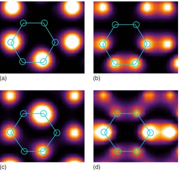
(5) PHYSICAL REVIEW B 80, 075115 共2009兲. LATTICE DEFECTS AND BOUNDARIES IN CONDUCTING…. (a). (a). (b). (c). (d). (b). (c). FIG. 5. 共Color online兲 The expected STM image for an armchair tube with perfectly cut edges. A section near the right edge of a tube of total length 30 nm is shown. 共a兲 Image corresponding to the excitation of the symmetric mode 共S兲 and 共b兲 of the antisymmetric channel 共A兲. 共c兲 Color scale of all STM images in arbitrary units from 0 to unity.. are calculated by standard assumptions of an s-wave orbital on the tip and orbitals for the nanotube. For the images presented here we use the parameters given in Ref. 41 in arbitrary units for the tunneling current. In order to show the resulting impurity effects with a maximum resolution we choose a very small distance ⱗ1 Å of the STM tip to the sample. Larger distances naturally result in plots with less resolution but look qualitatively the same. Orbital mixing and geometric distortion due to the nanotube curvature can also be taken into account40–42 but here the STM images are projected onto a flat surface in order to explicitly demonstrate the main effects of the defects. The procedure above basically determines the LDOS of the nanotube by using the square of the eigenstates in the effective models. In Fig. 5 we show an example for a finite armchair tube of 30 nm with sharp edges which corresponds to 240 lattice sites in each chain of the effective model. The symmetric 162 共E ⬇ 74 meV兲 and the antisymmetric mode for ky = 241 159 mode for ky = 241 共E ⬇ 93 meV兲 are shown. Here the energies are given relative to half filling and we used hopping parameters which correspond to the accepted Fermi velocity of v ⬇ 8.1⫻ 105 m / s. The energy spacing for a finite tube of 30 nm is about 55 meV for each mode 共chain兲. For the armchair tube the symmetric and antisymmetric modes are not degenerate. For the zigzag tube the two modes are degenerate but impurities and defects generally lift the degeneracy. For example, in a 30 nm zigzag tube the cap described below in Sec. III B lifts the degeneracies by ⌬E ⬃ 10 meV whereas a single vacancy on the same tube will have a much smaller. FIG. 6. 共Color online兲 ARMCHAIR: Expected density patterns from an STS experiment. The axis of the tube is the horizontal direction. 共a兲 Image corresponding to the excitation of the symmetric mode 共S兲 close to the edge of the nanotube. 共b兲 Excitation of 共a兲 is now phase shifted by = / 2. 关共c兲–共d兲兴 Same as 关共a兲–共b兲 but now for the antisymmetric channel 共A兲.. effect giving ⌬E ⬃ 0.1 meV. The color scale given in Fig. 5 has been used in all following STM images as well. In the STM experiment the LDOS can be measured via the differential conductance between the STM tip and the nanotube dI 共eV,rជ兲 ⬃ 兺 兩共Ei,rជ兲兩2 , dV 兩Ei−eV兩⬍␦. 共18兲. where ␦ is the energy resolution of the measurement. For short tubes individual states can be resolved, as was demonstrated in several experiments.9,10 For longer tubes it is still useful to consider individual eigenstates theoretically since the resulting experimental signal can always be constructed by a simple superposition of the nearly degenerate states. The impurity effect on the detailed discrete energy spectrum is not very easy to measure while the actual modification of the standing waves is much more visible, which we will discuss in this work. For the pure case as shown in Fig. 5 two main features can be observed. The short-range feature on the atomic scale is characteristic for the detailed boundary condition as well as for the phase of the wave function. A long-range feature shows a rotation of an overall phase of the wave function, which slowly changes the STM pattern along the chain. This long-range feature is not related to impurity effects and only depends on the energy relative to the half-filled Fermi points. In particular, the rate of change with position is always given by ⬇ 共k − kF兲⌬y, where k − kF ⬇ 共E − EF兲 / v. The short-range STM pattern on the other hand is characteristic for each mode 共symmetric or antisymmetric or a mix-. 075115-5.
(6) PHYSICAL REVIEW B 80, 075115 共2009兲. REYES, STRUCK, AND EGGERT. (a). (b) (a). (b). FIG. 8. 共Color online兲 ARMCHAIR: 共a兲 Added carbon atom at the end of the tube. 共b兲 Extra dimer at the edge.. (c). (d). FIG. 7. 共Color online兲 ZIGZAG: Density patterns for the degenerate s and a channels near EF. The phase is chosen to be = 0 and the tube axis is aligned in the horizontal direction. 共a兲 Image corresponding to the excitation of the s0 mode close to a perfect end of the tube. 共b兲 The state in 共a兲 is now dephased by = / 2 along the tube. 关共c兲–共d兲兴 Plots analogous to 关共a兲–共b兲兴 but now for the a0 channel.. ture兲. It is also an indication for the detailed boundary condition close to the defects. Typical density patterns for the symmetric and antisymmetric states are shown in Fig. 6 for an armchair tube 共enlargement from Fig. 5兲. The symmetric states show significant spectral weight on the circumferential bonds while the antisymmetric states always have nodes there. The short-range patterns are useful to classify the symmetry of the states and the overall phase, which only changes slowly along the chain as described above. Accordingly, the analysis of STM patterns close to boundaries and defects can be analyzed to classify the nature and symmetry of the perturbation as we will see later. For the zigzag tube the calculation of the STM images proceeds analogously. However, in this case the symmetric and antisymmetric states for the pure case are degenerate. For most impurities this degeneracy is lifted while still preserving the symmetry. However, the choice of the phase in Eqs. 共15兲 and 共18兲 is no longer arbitrary and depends on the detailed impurity model. Therefore, the analysis of the shortrange STM patterns for the zigzag tube gives important additional information. The characteristic short-range patterns of a finite tube are shown in Fig. 7 for s=0 and a=0. Other possible values of will be discussed in the context of defects.. III. CNT BOUNDARIES. In this section we examine the consequences of structures at the ends of SWCNTs on their electronic properties. The tubes can generally have different kinds of nonperfect edges. such as extra atoms at open ends, pentagons, or halffullerene caps that can crucially modify their behavior. In what follows we study this problem in the framework of the chain lattice models derived in Sec. II. This will illustrate how simple imperfect ends or even complex carbon structures that close the tube 共caps兲, can be easily incorporated to the effective Hamiltonians by adding only one or a few sites to the initial two chain models representing the clean nanotube. A. Armchair. The simplest nontrivial edge that can be introduced is the addition of a single carbon atom at an otherwise perfect open end 共clean cut兲 of a SWCNT as shown in Fig. 8共a兲. The extra site can be included in the full hopping Hamiltonian of an armchair tube in Eq. 共1兲 by an additional term † † + ␣x=2,y=L 兲c + H.c., HC = − t共x=1,y=L. 共19兲. where c represents the site of the additional carbon atom. Since the conduction bands only contain the k = 0 modes, using the approximation in Eq. 共2兲 the additional term simplifies to. HCeff = −. t. 冑N 关共y=L + ␣y=L兲c + H.c.兴 = − t †. †. 冑. 2 † 共S c + H.c.兲. N L 共20兲. Therefore, the electron on the extra site c hops to the symmetric S-mode chain while the antisymmetric mode is unmodified by the additional carbon atom as would be expected from the geometry of the problem. The effective hopping to the impurity weakens as the radius of the tube increases 共t⬘ = t冑2 / N兲 since the S mode is distributed homogeneously around the tube of which only two bonds couple to c. Another possible defect is the presence of an extra bond as shown in Fig. 8共b兲. In a similar way as above for the additional atom, the extra bond 共B兲 can be included into the effective model by adding. 075115-6.
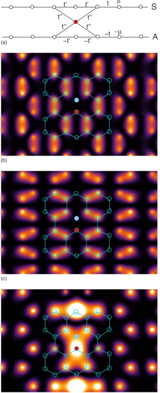
(7) PHYSICAL REVIEW B 80, 075115 共2009兲. LATTICE DEFECTS AND BOUNDARIES IN CONDUCTING…. HBeff = −. =−. t. †. t. †. 冑N 共y=L␣B + ␣y=LB + H.c.兲 − t共␣BB + H.c.兲, †. †. 冑N 关共SLSB − ALAB兲 + H.c.兴 − t共SBSB − ABAB兲. †. †. †. 共21兲. 共22兲. As a result the defect is incorporated by adding an extra site to both S and A modes with a weakened hopping amplitude t⬘ = t / 冑N. It can be easily checked that by systematically adding all possible bonds around the tube 共i.e., extending it兲, the resulting modification to the effective Hamiltonian will be a mere added site, as it should be. It is worth mentioning that none of the two defects considered so far connects the pair of chains of the effective model. An example of such mixing produced by a defect will be provided later in Sec. IV B 1. Therefore, the modification of the STS spectrum by the extra sites can be determined in a straightforward way: 共i兲 the extra carbon atom will have a finite spectral density only when a state corresponding to S is excited; otherwise it will be completely empty. 共ii兲 STS measurements performed over an extra bond are expected to yield the same density as the one measured over the bonds at the edge of a perfect nanotube, that is, extended by a / 2. Otherwise the pattern follows the pure case in Fig. 6 with only a slight shift of the phase . SWCNTs may also be closed at their ends by some carbon structure such as a half fullerene or a nanocone. The closure is made possible by the introduction of topological defects 共typically pentagons兲 which induce a bending in the carbon network. For the armchair CNT we focus here on the 共6, 6兲 nanotube closed by a half fullerene. The corresponding cap introduces six pentagon defects in order to close the tube, as it can be seen in Fig. 9共a兲. To add the caps to the effective model, the only necessary modification is the inclusion of two extra sites at each end of the S-mode chain. The first one of them represents the k = 0 mode of the ring formed by the atoms at the tip of the six pentagon defects near the end as shown in Fig. 9共a兲. The last site corresponds to the k = 0 mode of the hexagon at the top of the cap. The values of the hopping and chemical potential for each one of these extra sites will be different from the bulk values t⬘ = 冑2t, ⬘ = 0, t⬙ = t, and ⬙ = 2t as indicated in Fig. 9. Due to the pentagon defects of the cap, the chain corresponding to the antisymmetric mode is not modified by the addition of this structures at the ends of the tube. It is easy to understand this by considering that the atoms at the tips of the pentagon defects are added in the same way as explained in Eq. 共20兲 for a single pentagon. In this picture the A mode becomes then completely decoupled from the half-fullerene cap.43 As a result, the effective lattice model that includes the cap looks like the one depicted in Fig. 9共b兲. Although we have here outlined the procedure for the specific cap shown in Fig. 9共a兲, the same basic ideas can be applied to construct effective models for nanotubes of larger radius. Capping structures for such tubes will, in general, be composed by a larger number of carbon atoms; therefore, the resulting effective models will require more additional sites for its description.. (a). S A. (b). t. µ t’ µ’ t’’ µ’’. −t −µ. (c). (d). FIG. 9. 共Color online兲 ARMCHAIR: 共a兲 Half-fullerene cap at the end of a 共6, 6兲 carbon nanotube. 共b兲 Low-energy effective model for the 共6, 6兲 nanotube including a half-fullerene cap. The sites corresponding to the cap are shown in 共red兲 filled dots. The A mode is not modified by the cap. Parameters for the added sites are: t⬘ = 冑2t, ⬘ = 0, t⬙ = t, and ⬙ = 2t. 共c兲 Electronic density for an eigenstate of the symmetric 共S兲 mode, obtained using the effective model in 共b兲. For illustration purposes sites corresponding to the cap have been flattened out. 共d兲 Same as in 共c兲 but now for the A mode; as expected, the cap is empty in this case.. For the individual states near a capped nanotube very clear effects in an STS experiment are expected. Namely, if the applied voltage matches the energy of one of the states corresponding to the A mode, the cap will appear completely empty. On the other hand, exciting a symmetric state would be clearly recognizable by the appearance of a finite amount of electron density distributed over the cap. Our density maps 共simulated STM images兲 clearly illustrate this effect as shown in Figs. 9共c兲 and 9共d兲. The density over the body of the tube is distributed very similar to the pure case in Fig. 6.. 075115-7.
(8) PHYSICAL REVIEW B 80, 075115 共2009兲. REYES, STRUCK, AND EGGERT. (b). (a). (a). FIG. 10. 共Color online兲 ZIGZAG: 共a兲 A vacancy at the edge of the tube. 共b兲 Extra dimer producing a pentagon defect at one end of the CNT.. s. B. Zigzag. a. As already mentioned in Sec. II B there is an arbitrary phase that defines the transformation to the effective two chain models. In what follows we will choose for each structural defect that we treat in such a way that their corresponding low-energy models are as simple as possible. We first consider the absence of a carbon atom at the end as illustrated in Fig. 10共a兲. This sort of imperfection involves the elimination of a pair of bonds that joined the missing atom at site l = 1 with a pair of atoms at l = 2 plus the addition of an extra hopping matrix between them. The resulting effective impurity Hamiltonian for such a vacancy 共V兲 is HVeff =. (b). µ=0 µ=0. t t. µ’ −3µ ’. t’ t. µ=0 µ=0. t0 tπ. µ’’ −µ’’. (c). 2t † t 共s s/6,2 + H.c.兲 − 共s† /6,2s/6,2 − 3a† /6,2a/6,2兲, N /6,1 N 共23兲. where we have chosen = / 6. The first term corresponds to the elimination of the atom and the second to the inclusion of the extra bond shown in Fig. 10共a兲. Another possible defect is the addition of an extra bond as the one shown in Fig. 10共b兲. In the effective models it is represented by couplings of both chains to the bond sites, corresponding to the impurity Hamiltonian HBeff = t共b−†b− − b+†b+兲 −. t. 冑N 共. † † 冑3s0,1 b− − ia0,1 b+ + H.c.兲,. 共24兲. (d). FIG. 11. 共Color online兲 ZIGZAG: 共a兲 Half-fullerene cap at the end of a 共9,0兲 CNT. 共b兲 Low-energy effective model for the conducting zigzag nanotube including the half-fullerene cap with parameters as defined in Eq. 共27兲. The last site of the s 共a兲 chain corresponds to the k = 0 共k = 兲 mode of the hexagon located at the top of the cap structure. 共c兲 Local density of states for an s/6 state and 共d兲 for an a/6 state.. where, † = b⫾. b†1 ⫾ b†2. 冑2. ,. 共25兲. and b1,2 are the sites of the extra bond. We note that the choice = 0 keeps the two modes completely decoupled even in the presence of a bond defect at the edge. Therefore, the STS signal will look very similar as in the pure case in Fig. 7 共except for a small change in the phase along the chain兲. To demonstrate the inclusion of a structure that closes the tube, we focus on the case of the 共9,0兲 nanotube depicted in. Fig. 11共a兲. Such a half-fullerene cap can be constructed starting from the perfect CNT in the following way: first, three vacancies are introduced at one end 共l = 1兲, each one of them producing a pentagon defect as the one discussed above for the vacancy. Then, each one of the six remaining atoms at the end is linked to the atoms that form the hexagon at the top of the cap. Choosing again = 6 it turns out that each one of the aforementioned “cap vacancies” correspond exactly to a term like the one obtained above, in such a way that the part of the cap Hamiltonian corresponding to all three of them is. 075115-8.
(9) PHYSICAL REVIEW B 80, 075115 共2009兲. zigzag. zigzag. LATTICE DEFECTS AND BOUNDARIES IN CONDUCTING…. (a). (b). armchair. armchair. FIG. 12. 共Color online兲 Two types of defects in the bulk of carbon nanotubes. The arrows indicate the direction of the axis for the two classes of tubes. 共a兲 Stone-Wales defect formed by a pair of pentagon-heptagon deformations. Defective sites are depicted by filled 共red兲 dots and they correspond exactly to the ones added to the effective model. 共b兲 Vacancy defect produced by taking away a single carbon atom, breaking the ␣- sublattice symmetry. The big dot 共blue兲 represents the missing atom also in the following figures.. 共26兲. HCVeff = 3HVeff .. Furthermore, it can be shown that the s/6 and a/6 channels of the effective model couple only to the k = 0 and k = † modes 共d0, 兲 of the hexagon at the top of the cap. The resulting effective Hamiltonian for the cap of the 共9,0兲 nanotube becomes HCAP = HCVeff + 2t共d† d − d†0d0兲 +. t. 冑3 共s/6,1d0 − i †. 冑3a† /6,1d 共27兲. + H.c.兲, where, dk =. 1. 6. d je 冑6 兺 j=1. ikj. 共28兲. and d j are the sites of the hexagon at the top of the cap. By conveniently choosing = / 6 we have again managed to express the Hamiltonian in terms of two completely decoupled modes even when the cap is present. The resulting model requires the addition of a couple of sites and a local change in the values of the parameters as it is illustrated in Fig. 11共b兲. As for the armchair nanotube, we have described here the procedure only for one specific cap. Nevertheless, the same scheme can be followed to model caps of tubes of larger radius that will naturally require a greater number of extra sites in the effective model. The LDOS around the cap of the 共9,0兲 nanotube is displayed in Figs. 11共c兲 and 11共d兲 for two different energies near the Fermi level. In this case both s and a states have a finite density at the cap. Notice that due to the = / 6 phase shift the forms of the patterns are inverted relative to Fig. 7; the ones of s/6 共a/6兲 look like the ones of a0 共s0兲. This can be easily understood from Eq. 共15兲 since the shift of = / 6 together with a translation of one site around the tube converts the cosine and sine functions into one another. The effect is clear when comparing Fig. 7 with Fig. 11.. IV. DEFECTS IN THE BULK. The honeycomb structure composing the CNT may present a variety of structural defects which are known to significantly modify its electronic properties.18,19 It is possible to model any kind of defect in a straightforward way using the chain lattice models introduced in Sec. II. As an example we will show explicitly how to include two prototypical impurity models: the Stone-Wales 共SW兲 and the single vacancy defects as shown in Fig. 12. We first show how the low-energy models look once the defects are included and then use them to obtain electron densities for the states closest to the Fermi energy. As already mentioned in Sec. I, relaxation35 will, in general, also occur around defects which cannot be implemented in the formalism without additional input from ab initio calculations. Nonetheless, the examples we consider here demonstrate the general method also for more complicated cases and also show the most relevant effects that are expected from impurities of this symmetry class. A. Stone-Wales defect. One of the simplest deformations that can be introduced to the perfect graphene lattice is a pair of pentagon-heptagon defects as the one shown in Fig. 12共a兲. These are usually called 共Ref. 44兲 SW or 5-7-7-5 defects and can be thought of as a simple 90° rotation of a single bond. Stone-Wales defects have low energy and they do not modify the helicity of the tube. They are also known to be responsible for the initiation of the plastic deformation of CNTs as the bond aligns in the direction of the applied strain.45 1. Armchair. Incorporation of the 5-7-7-5 defect to the effective model of the armchair nanotube is achieved by adding a couple of sites that are connected to the S-mode chain with the parameters t⬘ = t共N − 1兲 / N , ⬘ = 共N − 1兲 / N , t⬙ = t冑2 / N as shown. 075115-9.
(10) PHYSICAL REVIEW B 80, 075115 共2009兲. REYES, STRUCK, AND EGGERT. t. t+. t’’. t’’ t’. (a). t. µ’ t’. −t’ −µ’. −t’. t. µ. S. t− t. −t. (a). −µ. t’. t. b+. t’ b−. t. t+ t’. s. t− t. a. A. (b) (b). (c) (c). FIG. 13. 共Color online兲 ARMCHAIR: 共a兲 Effective lattice model including the Stone-Wales defect. The extra sites 共in red兲 correspond to the two carbon atoms of the defective bond. Some hopping amplitudes and chemical potentials are modified around the deformation: t⬘ = t共N − 1兲 / N , ⬘ = 共N − 1兲 / N , t⬙ = t冑2 / N. 共b兲 Electron density around the defect for the S state at the Fermi level. As expected, there is a finite occupation of the defective bond. 共c兲 Same as in 共b兲 but now for the A state. The defective bond is now completely empty.. in Fig. 13共a兲. This can be derived in two steps: first, eliminating one bond has the effect of locally weakening the hopping and chemical potential of the effective chain sites. Then, the rotated bond is included by adding a couple of extra sites corresponding to the atoms of the defective bond. As pointed out above, the pentagon defects along the tube are not seen by the antisymmetric mode; therefore, the second step does not modify the A chain. Again, there are interesting effects that can be observed in simulated STM images. Tuning the voltage to an energy corresponding to an eigenstate of the S channel, these sites will be significantly occupied as seen in Fig. 13共b兲. Otherwise, if the applied voltage matches the energy of the antisymmetric mode, the defective bond will appear as completely empty as shown in Fig. 13共c兲. In both cases, away from the defect the. FIG. 14. 共Color online兲 ZIGZAG: 共a兲 Effective lattice model for the zigzag tube including the Stone-Wales defect. Additional sites correspond to the symmetric 共b+兲 and antisymmetric 共b−兲 modes of the defective bond. The values for the locally modified parameters are t⬘ = t共N − 1兲 / N, t+ = t / 冑N, and t− = ⫾ i冑3t+. The hopping direction in which t− has a positive sign is indicated by arrows to b−. 共b兲 Electron density around the defect for a s/6 state close to the Fermi level. 共c兲 Same as in 共b兲 but now for a a/6 state.. density pattern will look essentially identical to the one of the perfect tube as shown in Fig. 6. 2. Zigzag. The situation for the zigzag tube is rather different. First we choose = / 6 for the modes s and a in the transformation Eq. 共15兲 since it yields the simplest possible lowenergy model. In such a basis the elimination of a bond translates into a weakening of a few hopping elements of the s chain but leaves a intact. Furthermore, the subsequent addition of the defective bond involves connecting the s共a兲 channel to the b+共b−兲 mode of the added bond, where b⫾ is defined by Eq. 共25兲. The resulting form of the effective model with the parameters t⬘ = t共N − 1兲 / N, t+ = t / 冑N, and t− = ⫾ i冑3t+ is shown in Fig. 14共a兲. Patterns obtained from an STM experiment around the imperfection for energies close to the Fermi level are ex-. 075115-10.
(11) PHYSICAL REVIEW B 80, 075115 共2009兲. LATTICE DEFECTS AND BOUNDARIES IN CONDUCTING… t’. t’. t’’. t’’ t’’. t’’. (a). −t’. −t’. t. µ. −t −µ. pected to look like Figs. 14共b兲 and 14共c兲. Depending on the symmetry of the state and the position of the defect, the Stone-Wales bond can be observed to accumulate a large amount of density as in Fig. 14共c兲 or in other cases become completely empty as in Fig. 14共b兲. Unlike for the armchair case, in the zigzag CNT the lack of density on the defective bond is not an exclusive property of a state with a certain symmetry.. S A. B. Vacancy defect. Irradiation of a carbon nanotube by Ar+ ions may result in the presence of metastable but long-lived single vacancy defects on its surface46 as illustrated in Fig. 12共b兲. The absence of an atom in the carbon network obviously does not change the overall chiral vector of the tube but it will still have some pronounced consequences on its electronic properties. For example, recent theoretical21 and experimental20,22 works have shown that nanotubes enter the strong Anderson localization regime when the concentration of defects is large enough.. (b). 1. Armchair. (c). (d). FIG. 15. 共Color online兲 ARMCHAIR: 共a兲 The vacancy is included into the low-energy effective lattice model. An extra site represents the nearest neighbor of the vacancy in the direction perpendicular to the tube’s axis. Parameters are modified around the imperfection: t⬘ = t共N − 1兲 / N , ⬘ = 共N − 1兲 / N , t⬙ = t / 冑2N. 共b兲 Electron density around the defect for an eigenstate which looks basically exactly the same as one corresponding to the pure symmetric channel 共S-type兲. 共c兲 Same as in 共b兲 but now the density looks as the one of the A mode 共A-type兲. 共d兲 There is a third group of eigenstates that combine both channels in such a way that the density is accumulated in one of the sublattices; this is a manifestation of the broken sublattice symmetry by the vacancy defect.. To include the vacancy in the effective chain model a single extra site must be added, which corresponds to the remaining atom of the defective bond with coupling parameters t⬘ = t共N − 1兲 / N , ⬘ = 共N − 1兲 / N , t⬙ = t / 冑2N as shown in Fig. 15共a兲. It is interesting to note that this time the S and A chains become connected as a consequence of the introduction of the defect. Therefore, eigenstates will not necessarily correspond to the electron occupying a single mode but they will, in general, be a mixture of both. It turns out that there are now three types of possible states: S-type, A-type, and mixed 共M兲. The first two correspond to states in which the electron occupies primarily only one of the original channels as illustrated in Figs. 15共b兲 and 15共c兲. Mixed states are also possible, where the eigenstate is a linear combination of the S and A modes. It is found that the M states completely break the sublattice symmetry of the hexagonal lattice, resulting in an accumulation of the electron density on the sublattice opposite to the one of the vacancy as shown in Fig. 15共d兲. It appears that the effective extra site enables a resonance at certain energies. A related effect of a strongly enhanced spectral weight around vacancies at certain energies has been predicted for graphene using a linearized band structure.47 For quantitative estimates more realistic microscopic models must also take relaxation effects into account which are especially important for vacancy defects. This will generally modify the couplings and STM images in a finite range but the resulting eigenstates can be classified into one of the three types 共A兲, 共S兲, or 共M兲 with the characteristic general properties as shown in Fig. 15. 2. Zigzag. For the case of the zigzag nanotube, the vacancy does not require an additional site in the effective model since it represents only a slight modification on one effective chain lattice site. In this case, the choice = / 6 again yields the. 075115-11.
(12) PHYSICAL REVIEW B 80, 075115 共2009兲. REYES, STRUCK, AND EGGERT. t. (a). t. t’. t. t’. t. t. t. s a. (b). (c). FIG. 16. 共Color online兲 ZIGZAG: 共a兲 Chain lattice model including the vacancy defect. There is a slight weakening of the hopping along the s/6 channel from t to t⬘ = t共N − 1兲 / N. 共b兲 Local density of states around the imperfection for a level corresponding to the s/6 chain. 共c兲 Density pattern around the vacancy for an a/6 state.. simplest effective model. In fact only the s/6 mode is modified by the presence of a vacancy which causes a slight weakening of local hopping terms t⬘ = t共N − 1兲 / N as shown in Fig. 16共a兲. We note that the same impurity terms were also present when we considered the Stone-Wales defect, which is not surprising given that it is nothing more than two consecutive vacancies plus the attachment of the defective bond. As seen in Figs. 16共b兲 and 16共c兲, the broken sublattice symmetry is not manifest in the density patterns. Nevertheless, the presence of the vacancy has the effect of pinning the phase of the wave function around the nanotube. Remarkably, the antisymmetric channel is not at all affected by the vacancy, except of course for the missing spectral weight at the vacancy. As discussed before, the choice of = / 6 makes the antisymmetric state appear like the = 0 symmetric state in Fig. 7 and vice versa. As mentioned above relaxation is important also in the zigzag case. However, since the parity symmetry of the system is not broken by a vacancy in the zigzag tube the channels are bound to remain decoupled and the general classification in Fig. 7 still holds.. V. SUMMARY AND OUTLOOK. In summary, we have shown how defects and capping structures can be added to effective two chain models of conducting SWCNTs. We have demonstrated the method by incorporating half-fullerene caps and Stone-Wales and vacancy defects to both the armchair and conducting zigzag nanotubes. Using the resulting chain lattice models of the conduction bands we obtained the LDOS around the imperfections for states close to the Fermi level. Besides their simplicity the most remarkable feature of the effective models is the fact that the two chains are completely decoupled and also remain decoupled even in the presence of most defects and additional structures at the end considered here. Especially in the zigzag case, the defects in fact dictate the proper choice of the basis, which then represent the two independent channels. Surprisingly, a single vacancy leaves all states in the antisymmetric channel of metallic zigzag CNTs completely unchanged. Therefore, transport in that channel should be possible without scattering, which may have strong consequences for the resulting conductivity. However, this reduction in scattering is only possible if vacancies are spaced so that they do not affect each other and if there are no other strong perturbations which would pin the phase around the tube. Interactions will introduce a coupling between the independent chains as discussed in the Appendix but of course even in that case it is useful to start in the basis of decoupled chains. At this point it should be emphasized that the methods presented above are not restricted to the examples explicitly shown here but the transformations in Sec. II give a quite general framework which allows for the treatment of a wide range of possible imperfections. For example, the procedure illustrated in the present paper can be extended to tackle problems such as junctions of 共conducting兲 CNTs of different chirality, presence of magnetic impurities, or transport related problems, just to mention a few interesting prospects. From the point of view of applications, it is clear that this approach can be useful to assess the effect that a particular deformation or impurity has on the electronic properties of nanotubes in a very simple and precise manner. It is thus a promising tool to be employed for the design of CNT-based microelectronic devices. On the other hand, from a more fundamental perspective, since the resulting models are one dimensional, it will be certainly interesting to take into account strong correlation effects in future works by using the techniques available for such systems 共i.e., bosonization or DMRG兲. ACKNOWLEDGMENTS. We are thankful for discussions with Michael Bortz, Imke Schneider, and Stefan Söffing. Financial support was granted by the Deutsche Forschungsgemeinschaft via the Transregio 49 “Condensed Matter Systems with Variable Many-Body Interactions.” APPENDIX: INTERACTIONS. In the main text we have neglected interactions between electrons and worked exclusively with the resulting free-. 075115-12.
(13) PHYSICAL REVIEW B 80, 075115 共2009兲. LATTICE DEFECTS AND BOUNDARIES IN CONDUCTING…. electron models. We will now show that including interactions into the effective Hamiltonian can be done in a straightforward way. Although, in principle, we could consider any electron-electron potential, for definiteness we will treat only on-site density-density interactions 共U兲. To illustrate how a defect modifies the interacting term, we will explicitly show the case of the Stone-Wales deformation.. ↑ ↓ ↑ ↓ Hint b = U共nb nb + nb nb 兲. 1. The interaction Hamiltonian for the zigzag CNT is, Hint = U 兺 c†j,l↑c j,l↑c†j,l↓c j,l↓ .. 共A1兲. Using the two-band approximation and transformation in Eq. 共14兲 the effective interaction term becomes, int = Heff. U 兺 共␣†y,↑␣y,↑␣†y,↓␣y,↓ + †y,↑y,↑†y,↓y,↓兲. 共A2兲 N y. U ↑ ↓ ↑ ↓ 共y兲nAA 共y兲 + nSA 共y兲nSA 共y兲 兺 关n↑ 共y兲nSS↓ 共y兲 + nAA 4N y SS ↑ ↓ ↑ ↓ ↑ ↓ 共y兲nAS 共y兲 + nSS 共y兲nAA 共y兲 + nAA 共y兲nSS 共y兲 + nAS ↑ ↓ ↑ ↓ + nSA 共y兲nAS 共y兲 + nAS 共y兲nSA 共y兲兴,. 共A3兲. where, nPQ = P† Q .. 共A4兲. As we can see, even though rewriting the Hamiltonian in terms of the S and A modes simplifies its noninteracting part, the interaction terms become more convoluted. It is interesting to note that the effective on-site interaction becomes inversely proportional to the number of bonds around the tube 共Ueff = U / 4N兲. Such a dependence is not surprising: the occupation of a site in one of the effective low-energy channels represents the presence of a single electron distributed around the tube’s N bonds. To include the Stone-Wales defect we first note that a 共normal兲 bond around the nanotube is missing and there is thus a slight decrease in the on-site interaction at the corresponding site, Ueff共y d兲 =. 共N − 1兲 Ueff . N. 共A5兲. Furthermore, we have to add the interaction terms that act on the added 共defective兲 bond,. U ↑ ↓ ↑ ↓ ↑ ↓ 共l兲n++ 共l兲 + n−− 共l兲n−− 共l兲 + n++ 共l兲n−− 共l兲 兺 关n++ N l ↑ ↓ ↓ ↑ ↓ ↑ 共l兲 + n−+ 共l兲n+− 共l兲兴, 共l兲n++ 共l兲 + n+− 共l兲n−+ + n−−. 共A8兲. where,. In terms of the S and A modes this term looks slightly more complicated, int = Heff. 共A7兲. j,l. Using Eq. 共2兲 the conduction-band part becomes, int = Heff. 共A6兲. 2. 2. Zigzag. For the armchair carbon nanotube an on-site interaction is given by rជ. 2. Remarkably, while the interaction in the bulk of the tube is reduced by a factor of 1 / N in Eq. 共A3兲, the effective interaction on the Stone-Wales bond is not rescaled and therefore is bound to play a much stronger role.. 1. Armchair. Hint = U 兺 共␣rជ†,↑␣rជ,↑␣rជ†,↓␣rជ,↓ + rជ†,↑rជ,↑rជ†,↓rជ,↓兲.. 1. n = C† ,C, .. 共A9兲. We find that the effective interaction is again inversely proportional to the tube’s circumference 共Ueff = U / N兲. Note also that the initially independent chains of Eq. 共13兲 become correlated by the scattering terms that involve both + and − modes. The first effect that the Stone-Wales defect will have on this model is a weakening of the interaction strength 共Ueff兲 similar to the one derived for the armchair tube but now it affects two contiguous sites, ld and ld + 1 共see Fig. 14兲. They will both have, Ũeff =. 共N − 1兲 Ueff . N. 共A10兲. Furthermore, a couple of terms of order O共N−2兲 arise, which contain local interaction vertices of a kind that was not present for the pure system, H̃int l =−. U ↑ ↓ ↑ ↓ ↓ ↑ ↓ ↑ 兲共l兲 n−+共l兲 − 共n++ + n−− 兲共n+− + n−+ 关n n 共l兲 + n−+ N2 +− +−. ↓ ↓ ↑ ↑ 兲共n+− + n−+ 兲共l兲兴, + n−− − 共n++. 共A11兲. one for each of the defective sites mentioned before 共l = ld , ld + 1兲. The last and most trivial part of the interaction term coming from the impurity corresponds to the on-site terms of the defective bond. Such a term will be exactly the same as the one given for the armchair carbon nanotube in Eq. 共A6兲, again with a not rescaled stronger interaction strength.. 075115-13.
(14) PHYSICAL REVIEW B 80, 075115 共2009兲. REYES, STRUCK, AND EGGERT S. Iijima and T. Ichihashi, Nature 共London兲 363, 603 共1993兲. S. Bethune, C. H. Kiang, M. S. de Vries, G. Gorman, R. Savoy, J. Vazquez, and R. Beyers, Nature 共London兲 363, 605 共1993兲. 3 For a review on the electronic properties of SWCNTs see J.-C. Charlier, X. Blase, and S. Roche, Rev. Mod. Phys. 79, 677 共2007兲. 4 C. L. Kane and E. J. Mele, Phys. Rev. Lett. 78, 1932 共1997兲. 5 A. Kleiner and S. Eggert, Phys. Rev. B 63, 073408 共2001兲. 6 A. Rubio, D. Sanchez-Portal, E. Artacho, P. Ordejon, and J. M. Soler, Phys. Rev. Lett. 82, 3520 共1999兲. 7 A. Rochefort, D. R. Salahub, and P. Avouris, J. Phys. Chem. B 103, 641 共1999兲. 8 J. Jiang, J. Dong, and D. Y. Xing, Phys. Rev. B 65, 245418 共2002兲. 9 L. C. Venema, J. W. G. Wildoer, J. W. Janssen, S. J. Tans, H. L. J. Temminck Tuinstra, L. P. Kouwenhoven, and C. Dekker, Science 283, 52 共1999兲. 10 S. G. Lemay, J. W. Jansen, M. van den Hout, M. Mooij, M. J. Bronikowski, P. A. Willis, R. E. Smalley, L. P. Kowenhoven, and C. Dekker, Nature 共London兲 412, 617 共2001兲. 11 F. Anfuso and S. Eggert, Phys. Rev. B 68, 241301共R兲 共2003兲. 12 I. Schneider, A. Struck, M. Bortz, and S. Eggert, Phys. Rev. Lett. 101, 206401 共2008兲. 13 J. Lee, S. Eggert, H. Kim, S.-J. Kahng, H. Shinohara, and Y. Kuk, Phys. Rev. Lett. 93, 166403 共2004兲. 14 S. Eggert, Phys. Rev. Lett. 84, 4413 共2000兲. 15 Y. F. Fan, B. R. Goldsmith, and P. G. Collins, Nature Mater. 4, 906 共2005兲. 16 J.-C. Charlier, T. W. Ebbesen, and Ph. Lambin, Phys. Rev. B 53, 11108 共1996兲. 17 L. Chico, L. X. Benedict, S. G. Louie, and M. L. Cohen, Phys. Rev. B 54, 2600 共1996兲. 18 H. J. Choi, J. Ihm, S. G. Louie, and M. L. Cohen, Phys. Rev. Lett. 84, 2917 共2000兲. 19 M. Bockrath, W. Liang, D. Bozovic, J. H. Hafner, C. M. Lieber, M. Tinkham, and H. Park, Science 291, 283 共2001兲. 20 J. Kong, E. Yenilmez, T. W. Tombler, W. Kim, H. Dai, R. B. Laughlin, L. Liu, C. S. Jayanthi, and S. Y. Wu. Phys. Rev. Lett. 87, 106801 共2001兲. 21 B. Biel, F. J. García-Vidal, A. Rubio, and F. Flores, Phys. Rev. Lett. 95, 266801 共2005兲. 1. 2 D.. 22. C. Gómez-Navarro, P. J. de Pablo, J. Gómez-Herrero, B. Biel, F. J. García-Vidal, A. Rubio, and F. Flores, Nature Mater. 4, 534 共2005兲. 23 Y.-W. Son, J. Ihm, M. L. Cohen, S. G. Louie, and H. J. Choi, Phys. Rev. Lett. 95, 216602 共2005兲. 24 A. R. Rocha, J. E. Padilha, A. Fazzio, and A. J. R. da Silva, Phys. Rev. B 77, 153406 共2008兲. 25 J.-Y. Park, Appl. Phys. Lett. 90, 023112 共2007兲. 26 A. Bachtold, P. Hadley, T. Nakanishi, and C. Dekker, Science 294, 1317 共2001兲. 27 P. Avouris, Z. Chen, and V. Perebeinos, Nat. Nanotechnol. 2, 605 共2007兲. 28 D. C. Mattis, Phys. Rev. Lett. 32, 714 共1974兲. 29 C. L. Kane and M. P. A. Fisher, Phys. Rev. Lett. 68, 1220 共1992兲. 30 S. Eggert and I. Affleck, Phys. Rev. B 46, 10866 共1992兲. 31 C. L. Kane and E. J. Mele, Phys. Rev. B 59, R12759 共1999兲. 32 S. Rommer and S. Eggert, Phys. Rev. B 62, 4370 共2000兲. 33 L. Balents and M. P. A. Fisher, Phys. Rev. B 55, R11973 共1997兲. 34 H. H. Lin, Phys. Rev. B 58, 4963 共1998兲. 35 A. A. El-Barbary, R. H. Telling, C. P. Ewels, M. I. Heggie, and P. R. Briddon, Phys. Rev. B 68, 144107 共2003兲. 36 A. O. Gogolin, A. A. Nersesyan, and A. M. Tsvelik, Bosonization and Strongly Correlated Systems 共Cambridge University Press, Cambridge, England, 1998兲. 37 S. R. White, Phys. Rev. Lett. 69, 2863 共1992兲. 38 R. Egger and A. O. Gogolin, Phys. Rev. Lett. 79, 5082 共1997兲. 39 C. Kane, L. Balents, and M. P. A. Fisher, Phys. Rev. Lett. 79, 5086 共1997兲. 40 A. Kleiner and S. Eggert, Phys. Rev. B 64, 113402 共2001兲. 41 V. Meunier and Ph. Lambin, Phys. Rev. Lett. 81, 5588 共1998兲. 42 I. Deretzis and A. La Magna, Nanotechnology 17, 5063 共2006兲. 43 States localized at the cap are also possible. Since they have high energy in general, we will not consider them here. 44 A. J. Stone and D. J. Wales, Chem. Phys. Lett. 128, 501 共1986兲. 45 P. Jensen, J. Gale, and X. Blase, Phys. Rev. B 66, 193403 共2002兲. 46 A. V. Krasheninnikov, K. Nordlund, M. Sirviö, E. Salonen, and J. Keinonen, Phys. Rev. B 63, 245405 共2001兲. 47 V. M. Pereira, J. M. B. Lopes dos Santos, and A. H. Castro Neto, Phys. Rev. B 77, 115109 共2008兲.. 075115-14.
(15)
Figure


+7


Documento similar
The general objective of this thesis is the development, characterization and application of solid contact ion selective electrodes (SC-ISEs) based on a layer of carbon
Interestingly, when using carbon nanotubes as the transducer material [7] for the detection of the same microorganism the differences between the covalent and the non-
We compare the mechanical properties of fibers made of polymers and of composites with pristine single-walled carbon nanotubes (SWNTs), mechanically interlocked
An Andreev reflection involves an electron incoming from the normal region into the superconducting one that is reflected as a hole, injecting a Cooper pair into the superconductor..
In this paper, we have calculated the LVR using only the mean value of the conductance for the random configurations at the Fermi level, an approximation that yields a
Here, we present the dual sensing and actuation performance of artificial muscles based on a conducting polymer and carbon nanotubes composite operated with triangular potential
The dispersion containing Single-Walled Carbon Nanotubes shows shear thinning effect, while aligned Multi-Walled Carbon Nanotubes in [EMIM][DCA] present shear thickening
Since for a regular ring R, the ideal lattice of R is iso- morphic to the congruence lattice of the principal right ideal lattice L of R, and since L has permutable congruences
