Studies on CIS thin Films Deposited by R F Sputtering and CdS Nanoparticles Deposited by Microwave Assisted CBD for Photovoltaic Aplications
134
0
0
Texto completo
(2) Este trabajo de tesis está dedicado a la memoria del. Dr. Hugo Alejo Velasco Molina Mentor y amigo entrañable …Yo lo miro desde lejos, pero somos tan distintos; es que creció con el siglo con tranvía y vino tinto… Viejo, mi querido viejo iii.
(3) AGRADECIMIENTOS Quiero reiterar mi eterno agradecimiento al apoyo que me dio en vida el Dr. Hugo Alejo Velasco Molina (q.e.p.d.) y mi eterna gratitud a su familia, en especial a la Sra. María Elena Aguirre Vda. de Velasco por todo el cariño y apoyo que durante años he seguido recibiendo y que me ha servido para alcanzar las metas más importantes de mi vida. Mi reconocimiento y sentido de gratitud está dedicado al Dr. Velumani Subramaniam, por su hábil dirección, paciencia, valiosas sugerencias y el estímulo constante a lo largo de mi investigación. Estoy muy agradecido con el Dr. Carlos Iván Rivera Solorio por su apoyo y sugerencias en la consolidación y estructuración de mis resultados. Es con gran satisfacción que aprovecho esta oportunidad para dejar constancia de mi sincero agradecimiento a la Sra. Alicia Garza la Güera de Navarro, quien a lo largo de mis estudios siempre me brindó su amistad y apoyo incondicional. También quiero agradecer al Dr. Bernard Micheli Masson por su apoyo y consejos en los momentos más difíciles durante mis estudios, al Dr. Federico Viramontes Brown por su constante motivación y acertadas recomendaciones y a la Dra. Oxana Vasilievna Kharissova por sus observaciones y consejos. Quiero agradecer al Dr. Mario Manzano Camarillo por darme la mano en los momentos difíciles y al Dr. Armando Llamas Terrés su firme apoyo para culminar mis estudios. Mi personal agradecimiento a los directores Dr. Pathiyamattom Joseph Sebastian, del CIE-UNAM, Temixco, al Dr. José Chávez Carvayar del IIM-UNAM, D. F., al Dr. Victor Sanchez Reséndiz del SEES-CINVESTAV, D. F. y al Dr. Umapada Pal del IFUAP, Puebla por su oportuna ayuda y sus esfuerzos para la caracterización y obtención de los resultados de las muestras analizadas. Mi sincero agradecimiento a los investigadores Dr. Arturo Morales Acevedo, Dr. Ramón Peña Sierra, Dr. Alejandro Ávila García, Dr. Iouri Alekseevich Koudriavtsev, Dr. Yasuhiro Matsumoto Kuwawara y Dra. Magali Estrada del Cueto, del Departamento de Ingeniería Eléctrica del SEES CINVESTAV-IPN, por proporcionarme los servicios de laboratorio necesarios y el estímulo constante a lo largo del curso de mi investigación. También quiero agradecer la excelente colaboración de varios miembros del Departamento de Ingeniería Eléctrica del SEES CINVESTAV-IPN en especial al M Sc. Miguel Galván Arellano, al Ing. Miguel Angel Avendaño, al Dr. Gaspar Casados Cruz y a la Ing. Georgina Ramírez Cruz por su excelente colaboración en las pruebas realizadas.. iv.
(4) Quiero agradecer de forma muy especial a Enriqueta Aguilar Valencia del SEES CINVESTAV-IPN por brindarme su amistad y por apoyarme en las numerosas deposiciones de los contactos de aluminio para las pruebas eléctricas. Mi más sincero agradecimiento al M Sc. Luis Ixtlilco Cortés y al Dr. Francisco Vallarta Rodríguez por su hospitalidad durante mis estancias en Temixco y el Distrito Federal, respectivamente. No encuentro palabras para agradecerle a mi compañera de estudios Vidhya Bhojan por todo el apoyo que proporcionó durante el curso de mi trabajo. Mi agradecimiento al M Sc. Ernesto Efrén Velázquez por dedicarle tiempo a la revisión y corrección de mi tesis para hacerla más elocuente. Mi más profundo agradecimiento a la Sra. Myriam Paloma Martínez Robles por haber sido como parte de mi familia durante mi preparación académica. Quiero expresar mi agradecimiento al Dr. Alberto Bustani Adem, rector del ITESM Campus Monterrey por la beca de sostenimiento que recibí durante mis estudios doctorales. De igual forma le agradezco al Dr. Hugo Terashima Marín por otorgarme una beca de excelencia y el apoyo económico para la titulación. Agradezco al proyecto “Agua y Vida”, a la cátedra de Nanoelectrónica, al Centro de Estudios de Energía y al Departamento de Becas del ITESM campus Monterrey por el apoyo económico brindado. Y por último y no menos importante le agradezco a Dios porque a pesar de los muchos y muy difíciles obstáculos que se me presentaron a lo largo de mi investigación y estudios, siempre surgió una solución para poder continuar y concluir mi doctorado.. v.
(5) RESUMEN La conversión de energía por medio de dispositivos fotovoltaicos es una alternativa viable para reducir las emisiones que contribuyen al calentamiento global. En la actualidad el silicio representa el principal material empleado en las celdas fotovoltaicas, el cual debe tener una pureza muy elevada y una estructura cristalina casi perfecta. Esto representa procesos muy caros que elevan el costo del producto y hace que la conversión de energía lumínica no sea una opción competitiva en comparación con la generación de energía por medio de combustibles fósiles. Las celdas fotovoltaicas de película delgada permiten reducir los costos de producción y adicionalmente crear celdas con un mínimo de material, reduciendo significativamente su costo. Materiales alternos al silicio como el cobre indio di-selenio (CIS) y el sulfuro de cadmio (CdS) prometen altas eficiencias combinadas con precios más bajos. El objetivo del presente trabajo de tesis es establecer las mejores condiciones de deposición para optimizar las propiedades de cada elemento que conforma una celda fotovoltaica completa. Una celda fotovoltaica se divide en cuatro capas principales: Contacto posterior (molibdeno) depositado por pulverización catódica en corriente directa, capa de absorción (CIS) depositada por pulverización catódica en radio frecuencia, capa ventana (CdS) depositado por baño químico asistido por microondas y contacto transparente superior (óxido de indio estaño) depositado por pulverización catódica en radio frecuencia.. Optimización de las propiedades estructurales, ópticas y eléctricas de la capa de absorción El CIS es un compuesto ternario que pertenece a la familia I-III-VI2 de los semiconductores. Se utiliza comúnmente como capa de absorción en sistemas fotovoltaicos en forma de película delgada policristalina. La técnica tradicional de deposición del CIS por pulverización catódica es empleando una fuente de corriente directa para depositar una película de CuIn y posteriormente hacer una selenización. En esta tesis se estudió la vi.
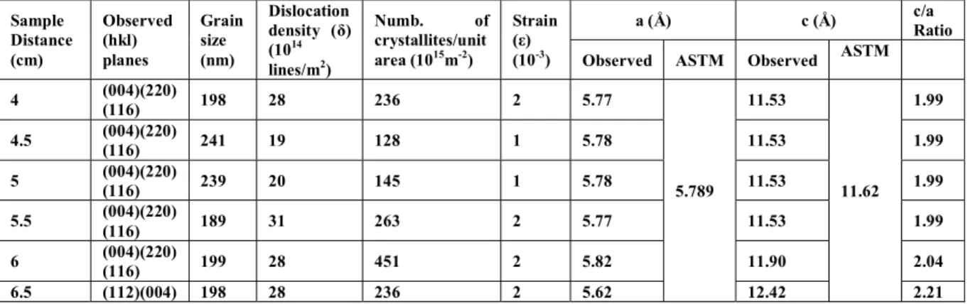
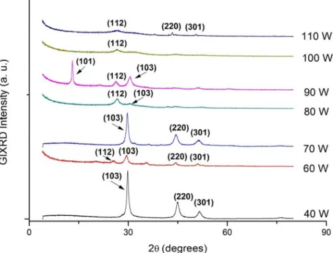
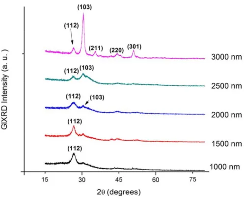
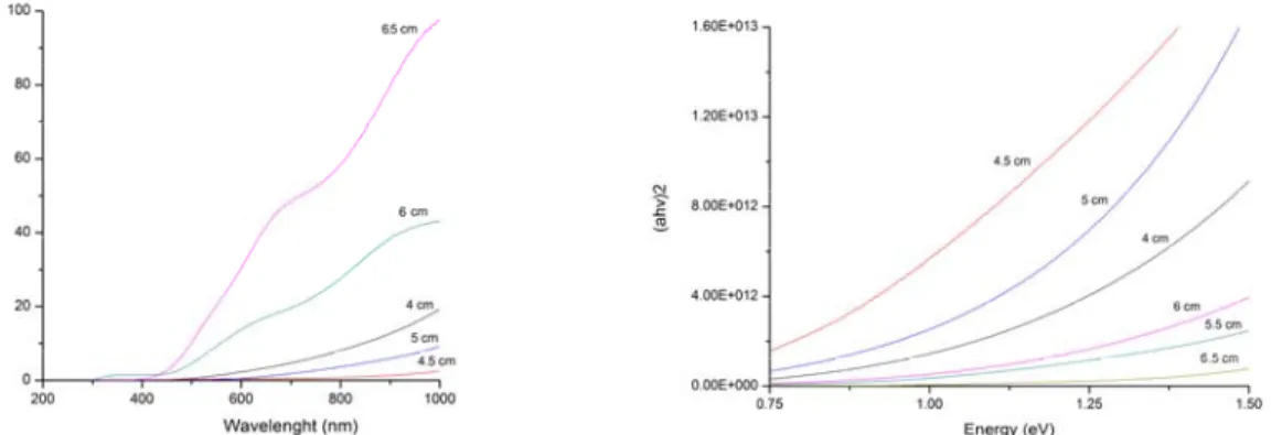
(6) deposición de CIS por medio de pulverización catódica a partir de un objetivo de CIS con 99.99% de pureza usando una fuente de radiofrecuencia. Los efectos de la variación de los parámetros distancia sustrato-objetivo, potencia y espesor fueron analizados. Las películas de CIS fueron depositadas por pulverización catódica en RF a partir de un único objetivo ternario de CuInSe2. Posteriormente se añadió una evaporación de cobre a las películas seguidas de recocido térmico adecuado para mejorar su cristalinidad y proporcionar adecuada estequiometría. El análisis estructural, de composición y morfología superficial se realizaron mediante difracción de rayos X (XRD), dispersión de energía de rayos X (EDAX) y análisis de microscopio electrónico de barrido (SEM), respectivamente. Se estudiaron las propiedades ópticas por medio de espectrofotometría usando longitudes de onda de 300 a 2500 nm. Las propiedades eléctricas se analizaron empleando la caracterización en conducción en corriente alterna (ac), corriente directa (I-V) y estudios de efecto Hall. La primer deposición de películas delgadas de CIS se basó en las condiciones del método tradicional y los parámetros fueron: espesor de 2000 nm, potencia de 80 W y se analizó el efecto de la distancia sustrato-objetivo de 4.0 a 6.5 cm. El análisis de composición mostró que las películas eran deficientes en cobre, por lo que se incorporó un proceso post-depósito que consistía en evaporar cobre por 13 segundos a una razón de crecimiento de 35Å/s y un tratamiento térmico a 500°C por 15 minutos. Posteriormente el análisis estructural indicó que todas las películas poseían estructura calcopirita con planos correspondientes a (112), (004), (220) y (116). Se observó un cambio en la preferencia del plano de (004) a (112) para la distancia máxima de sustrato-objetivo de 6.5 cm. El análisis de composición mostró que variando la distancia de 4.0 a 6.5 cm, el parámetro Δm = (Cu/In-1) pasó de -0.74 a 0.21 indicando que la difusión del elemento cobre mejora con la distancia, de tal forma que la mejor distancia entre el sustrato y el blanco fue 6.5 cm. El segundo grupo de películas se depositaron con un espesor de 2000nm, a una distancia sustrato-objetivo de 6.5 cm. y se varió la potencia de 40 a 110 W. La variación de potencia mostró un cambio muy significativo en las propiedades estructurales de las vii.
(7) películas, el tamaño de grano varió de 73 nm en la película depositada a 110 W hasta 287 nm en la película depositada a 40 W. Voltajes negativos fueron observados en el análisis del efecto hall en películas depositadas en potencias mayores a 90 W. El análisis óptico muestra que la película depositada a 80 W exhibía una brecha de energía directa que permite una absorción fotónica a partir de energías de 1.05 eV, el cual se considera adecuado para aplicaciones fotovoltaicas. El efecto Hall demostró que existe una relación entre la composición y el tipo de semiconductor. Se concluyó que el valor adecuado para la potencia era de 80 W. El tercer grupo de películas se depositaron variando el espesor de 1000 a 3000 nm a 80 W y distancia sustrato-objetivo de 6.5 cm. Los resultados estructurales mostraron que la orientación cambia del plano (112) al plano (103) en espesores superiores a los 2000 nm. Los análisis eléctricos mostraron que la mejor conductividad se da en las películas con orientación al plano (112) de esta forma se concluyó que el espesor óptimo era de 2000 nm debido a su orientación estructural.. Optimización de las propiedades estructurales, ópticas y eléctricas de la capa ventana El sulfuro de cadmio es un compuesto binario que pertenece a la familia II-VI de los semiconductores. Se emplea como capa ventana en las celdas fotovoltaicas policristalinas de película delgada. Películas delgadas de CdS policristalinas con brecha energía alrededor del 2.42 eV son hasta ahora la mejor capa ventana para heterouniones de CIS en celdas fotovoltaicas. Se elaboraron películas delgadas de CdS por un método rápido de síntesis llamado baño químico asistido por microondas (MA-CDB). Los compuestos químicos empleados en la deposición fueron: nitrato de cadmio (Cd (NO3) 2), citrato de sodio (Na3C6H5O7), Tiourea (CS (NH2)2) e hidróxido de amonio (NH4OH). Para las soluciones que contenían elementos de dopaje, se agregaron a la solución los siguientes reactivos: para el dopaje de cloro, 0.1M de cloruro de amonio (NH4Cl), para el dopaje de boro, 0.1M de ácido bórico (H3BO3), para el dopaje de sodio, 0.1M de cloruro sódico (NaCl). viii.
(8) Las películas delgadas de CdS se depositaron en sustratos de vidrio a 5 diferentes tiempos de depósito para generar 5 espesores distintos. Se adaptó a la unidad de microondas un control de la temperatura para mantener una temperatura constante de 70°C. El tiempo de irradiación de microondas fueron 60, 90, 120, 150 y 180 segundos con un tiempo de deposición total de 10, 15, 20, 25 y 30 minutos respectivamente. Los espesores de las películas depositadas se determinaron por un perfilómetro. La composición de las películas fue analizada utilizando EDAX. Se ha observado que la composición de las partículas de CdS fue prácticamente estequiométrica (42.17% atómico de azufre y 57.83% atómico de cadmio). Se determinaron las transmitancias ópticas de las películas por medio de un espectrofotómetro en un rango de longitudes de onda de 300 a 2500 nm. Los espectros de transmisión revelan un porcentaje relativamente alto de transmisión (80%) en las películas depositadas. La brecha de energía aumenta al aumentar el espesor. Se observaron brechas de energía de 2.46 eV a 2.54 eV. Las caracterizaciones eléctricas muestran que la conductividad aumenta de 270 a 4900S con el aumento en el espesor de 100 a 300 nm. Fotoluminiscencia, espectroscopía Raman y espectroscopía de masas de iones secundarios (SIMS) se emplearon para analizar las propiedades ópticas, estructurales y de composición respectivamente, de las películas de CdS al ser dopadas con Cloro, sodio y Boro. El análisis de fotoluminiscencia demostró que el cloro ha sido el elemento que más influye en el comportamiento del borde de banda. Los espectros de Raman de la película de CdS dopada con boro presentó una bien definida línea aproximadamente a 300 cm-1, que indican que este elemento fue absorbido en la estructura del CdS. SIMS mostró que la película de CdS dopada con boro tiene una mayor uniformidad a lo largo del espesor.. Optimización de las propiedades estructurales, ópticas y eléctricas del contacto superior transparente Oxido de indio estaño (ITO) usado como contacto superior transparente fue depositado por medio de pulverización catódica en radio frecuencia. La temperatura del sustrato, potencia y espesor fueron optimizados considerando las propiedades ópticas y eléctricas del ITO. El espesor de las películas depositadas de ITO que mostró mejor transmitancia y conductividad fue de 100 nm despositado a una temperatura de sustrato de ix.
(9) 100°C y a una potencia de 80W. La película presentaba una valor de transmitancia de 93% y una resistividad de 2.1x10⁻⁴ Ω.. Optimización de las propiedades estructurales y eléctricas del contacto posterior Las películas de molibdeno (Mo) empleadas como contacto posterior fueron depositadas por pulverización catódica en corriente directa. Se optimizaron las condiciones de deposición en base a las propiedades eléctricas. Las películas delgadas de Mo fueron depositadas sobre sustratos de vidrio variando el espesor de 400 a 1000 nm, la potencia de 20 a 40W y la temperatura de sustrato de temperatura ambiente a 500°C. La menor resistencia eléctrica se encontró en el espesor de 1000 nm con un valor de 6x10⁻⁴ Ω. Se observó que la resistencia disminuía al aumentar la temperatura del sustrato.. x.
(10) ABSTRACT The energy conversion via photovoltaic devices is a viable alternative for reducing emissions that contribute to global warming. At present, silicon is the main material used in photovoltaic cells, which must have a very high purity and an almost perfect crystal structure. This represents a very expensive process which increases the cost of the product and makes the conversion of light energy a not competitive option compared to energy generation through fossil fuels. Thin-film photovoltaic cells can reduce production costs and additional create cells with a minimum of material, reducing significantly its cost. Alternative materials to silicon such as copper indium di-selenide (CIS) and cadmium sulfide (CdS) promise high efficiencies, combined with lower prices. Present thesis work focuses on the deposition optimization of CIS, CdS, top and back contacts used in the fabrication of thin film photovoltaic devices. PV cell consists of four main layers: Contact later (molybdenum) deposited by direct current sputtering, absorber layer (CIS) deposited by radio frequency sputtering, window layer (CdS) deposited by microwave-assisted chemical bath and transparent top contact (indium tin oxide) deposited by radio frequency sputtering.. Optimization of structural, electrical and optical properties of the absorption layer CIS is a ternary compound that belongs to the I-III-VI2 family of semiconductors. It is commonly used as absorber layer in photovoltaic systems in the form of polycrystalline thin film. The traditional technique of the CIS deposition by sputtering is using a source of direct current to deposit a CuIn film and subsequently selenization. In this thesis we studied the CIS deposition by sputtering from a target of CIS with 99.99% purity using a radio frequency source. The effects of substrate to target distance, power and thickness were analyzed. CIS thin films were deposited by one-step sputtering from a single ternary target of CuInSe2. xi.
(11) Since the films were found to be deficit in copper, subsequently Copper granules has been evaporated on to the films and followed by thermal annealing to improve the crystallinity and provide adequate stoichiometry. Structural, composition and surface analysis were performed using X-ray diffraction, energy dispersive X-ray analysis and scanning electron microscope respectively. Optical properties were studied by spectrophotometer over the wavelength range of 300-2500 nm. Electrical parameters were evaluated by ac conduction, I-V characterization and Hall effect studies. The first set of CIS films were deposited based on traditional method and the parameters were: thickness of 2000 nm, 80W power and distance substrate target varied from 4.0 to 6.5 cm. Composition analysis showed that the films were deficit in elemental copper and therefore, in order to attain the stochiometry, an additional copper evaporation of 13 seconds at a rate of 35 Å/s and annealing of 15 minutes at 500°C were performed. Structural analysis indicates that all the films possess chalcopyrite structure with the peak values corresponding to (112), (004), (220) and (116). Shift in preferred orientation from (004) to (112) has been observed for the maximum substrate to target distance of 6.5 cm. From composition analysis it was found that by varying the distance from 4.0 to 6.5 cm, the parameter Δm = (Cu/In-1) has shifted from -0.74 to 0.21 indicating that diffusion of elemental copper improves with distance, thus it was found that the optimum distance between target and substrate was 6.5 cm. The second set of CIS thin films were deposited with a thickness of 2000 nm, substrate to target distance of 6.5 cm and power variation from 40 to 110 W. Change in power produces significant changes in structural properties of the films. Grain size varied from 73nm in a film deposited at 100W to 287 nm in a film deposited at 40W. Negative Hall voltage has been observed for films deposited above 90 W. Optical analysis shows that the film deposited at 80W exhibited a direct allowed transition with an average band gap value of 1.05 eV, which is considered appropriate to improve the conversion efficiency. Hall effect showed that there is a relationship between the composition and type of semiconductor. It was concluded that the appropriate value for the power was 80 W. xii.
(12) The third set of films were deposited with five different thicknesses from 1000 to 3000 nm at 80W and 6.5 cm substrate-target distance. Structural results showed that orientation changes from the plane (112) to plane (103) in thicknesses greater than 2000 nm. Electrical analysis showed that the best conductivity is in the orientation to the plane (112) and Optimum thickness was found to be 2000 nm due to the preferred oriented structure.. Optimization of structural, electrical and optical properties of the window layer Cadmium sulfide is a binary compound that belongs to the II-VI family of semiconductors. It is used as window layers in polycrystalline thin-film photovoltaic cells. CdS polycrystalline thin films with an energy band gap around 2.42 eV are now a day the best window layers for the CIS heterojunction photovoltaic cells. CdS thin films have been prepared by a rapid of microwave-assisted chemical bath deposition technique (MA-CBD) due to the ability of this technique to achieve homogeneous polycrystalline films in a few minutes instead of hours as it is in the conventional CBD. Chemical solution used for the deposition comprised of Cadmium Nitrate (Cd(NO3)2), Sodium Citrate (Na3C6H5O7), Thiourea (CS(NH2)2) and Ammonium Hydroxide (NH4OH). CdS thin films were deposited onto well-cleaned glass substrates for 5 different deposition times, thus varying the thicknesses of the deposited films. A temperature control is incorporated to the microwave unit to keep a constant temperature of 70°C. The total microwave irradiation times were 60, 90, 120, 150 and 180 seconds during deposition time of 10, 15, 20, 25 and 30 minutes respectively. Thicknesses of the deposited films were determined by a profile-meter. Composition of the films was analyzed using EDAX. It has been observed that the composition of CdS particles was Sulfur 42.17 atomic % and cadmium 57.83 atomic%. The sulfur deficit is expected due to CdS is nonstoichiometric semiconductor and this lack in sulfur allows n type conductivity. Both the cubic sphalerite (Hawleyite) and the hexagonal wurtzite (Greenockite) phases were observed by XRD analysis. Structural parameters such as lattice constants, crystallite size, dislocation density and strain have been evaluated. Optical transmittances of the films have xiii.
(13) been determined by spectrophotometer over wavelength range of 300-2500 nm. Transmission spectra reveal a relatively high transmission (80%) in the deposited films. Optical band gap increases with the increase in thickness. A direct band gap ranging from 2.46 eV to 2.54 eV was deduced. It was found that the electrical properties of CdS thin film can be extremely improve by doping, developing the recombination activity at the grain boundaries. Doping sources were added to the reactants to introduce elements to the films of chlorine, boron and sodium. The doping sources and concentrations added to the reactants were: for chlorine doping, 0.1M ammonium chloride (NH4Cl), for boron doping, 0.1M boric acid(H3BO3), for sodium doping, 0.1M sodium chloride (NaCl). Photoluminescence (PL), Raman spectroscopy and secondary ion mass spectroscopy (SIMS) analysis were performed to examine the optical, structural and composition respectively, of CdS films doped with chlorine, sodium and boron. PL analysis showed that chlorine has been the element that most influences the behavior of band edge. CdS films doped with chlorine presented a shift to the blue edge, indicating an opening of the absorption edge. Raman spectra of the boron doped CdS film present a well-resolved line at approximately 300 cm-1, which indicate that boron element has been absorbed into the CdS structure. SIMS showed the uniform incorporation of boron throughout the entire thickness of the deposited film. Electrical characterization shows that the conductivity increases from 270 to 4900S with the boron incorporation.. Optimization of structural, electrical and optical properties of the top contact layer Indium tin oxide used as front contact for PV devices were deposited by r.f. sputtering technique. Substrate temperature, power and thickness were optimized considering the optical and electrical properties of ITO. The best ITO layer thickness of the deposited films was in the range of 100 nm deposited at 100°C substrate temperature and power of 80W. This film obtained a maximum transmittance value of 93% and a resistivity of 2.1x10⁻⁴ Ω. xiv.
(14) Optimization of structural and electrical properties of the back contact layer Molybdenum films used as back contact layer were deposited by d.c. sputtering technique. The deposition conditions were optimized based on electrical properties. Mo thin films were deposited on glass substrates using DC sputtering varying the thickness from 400 to 1000 nm, power from 20 to 40 W and substrate temperature from room temperature to 500°C. The minimum resistance was found in 1000 nm thickness with a value of 6x10⁻⁴ Ω. It was observed that the resistance decreases with increasing substrate temperature.. xv.
(15) CONTENTS RESUMEN. ................................................................................................................. vi. ABSTRACT. ................................................................................................................. xi. CHAPTER I. Introduction............................................................................................... 1. 1.1. INTRODUCTION ............................................................................................... 1. 1.2. FOTOVOLTAIC CELLS ..................................................................................... 3. 1.2.1. SEMICONDUCTING COMPOUNDS ......................................................... 3. 1.2.2. P-N JUNCTION DEVICE ............................................................................ 4. 1.2.3. MATERIALS FOR PHOTOVOLTAIC CELLS ........................................... 6. 1.3. COPPER INDIUM DISELENIDE- Antecedents .................................................. 8. 1.4. CADMIUM SULFIDE-Antecedents .................................................................. 14. 1.5. CONCLUSIONS ............................................................................................... 17. REFERENCES ............................................................................................................ 19 CHAPTER II Experimental details ................................................................................ 26 2.1. INTRODUCTION ............................................................................................. 26. 2.2. PHYSICAL METHODS .................................................................................... 26. 2.2.1. R.F. SPUTTERING DEPOSITION ............................................................ 28. 2.2.2. SPUTTERING UNIT.................................................................................. 28 xvi.
(16) 2.2.3 2.3. SPUTTERING SET-UP.............................................................................. 30. CHEMICAL METHODS.................................................................................. 31. 2.3.1. CHEMICAL BATH DEPOSITION ............................................................ 31. 2.3.2. DEPOSITION OF CdS BY CBD ................................................................ 32. 2.2.3. MICROWAVE-ASSITED CHEMICAL BATH DEPOSITION .................. 33. 2.3.4. MA-CBD SET UP ...................................................................................... 34. 2.4. SUBSTRATE CLEANING ................................................................................ 34. 2.5. CHARACTERIZATION TECHNIQUES ......................................................... 36. 2.5.1. X-RAY DIFFRACTION TECHNIQUE...................................................... 36. 2.5.2. COMPOSITIONAL ANALYSIS ................................................................ 38. 2.5.3. SURFACE ANALYSIS .............................................................................. 39. 2.5.4. OPTICAL PROPERTIES ........................................................................... 40. 2.5.5. ELECTRICAL PROPERTIES .................................................................... 44. 2.5.6. RAMAN SPECTROSCOPY....................................................................... 47. 2.6. CONCLUSIONS ............................................................................................... 47. REFERENCES ............................................................................................................ 49 CHAPTER III Characterization of CIS absorber layer .................................................... 52 3.1. INTRODUCTION ............................................................................................. 52 xvii.
(17) 3.2. COMPOSITION, STRUCTURE AND SURFACE ANALYSIS ........................ 53. 3.2.1 3.3. OPTICAL PROPERTIES .................................................................................. 65. 3.3.1 3.4. Results and discussion ................................................................................ 54. Results and discussion ................................................................................ 66. ELECTRICAL PROPERTIES ........................................................................... 68. 3.4.1. AC conduction studies ................................................................................ 69. 3.4.2. Hall effect calculations ............................................................................... 71. 3.4.3. I-V results ................................................................................................... 73. 3.5. CONCLUSIONS ............................................................................................... 74. REFERENCES ............................................................................................................ 78 CHAPTER IV Characterization of window and contact layers ......................................... 81 4.1. INTRODUCTION ............................................................................................. 81. 4.2. CADMIUM SULFIDE (WINDOW LAYER) .................................................... 81. 4.2.1. STRUCTURE, COMPOSITION AND SURFACE ANALYSIS OF CdS ... 81. 4.2.1a. EFFECT OF THICKNESS ......................................................................... 82. 4.2.1b EFFECT OF ANNEALING ........................................................................ 87 4.2.2. OPTICAL CHARACTERIZATION ........................................................... 91. 4.2.2a. EFFECT OF THICKNESS ......................................................................... 91 xviii.
(18) 4.2.2b EFFECT OF ANNEALING ........................................................................ 93 4.2.3. ELECTRICAL CHARACTERIZATION .................................................... 94. 4.2.3a. PHOTO-RESPONSE .................................................................................. 94. 4.2.3b RESISTIVITY ............................................................................................ 96 4.2.4. DOPING..................................................................................................... 96. 4.2.4a. PHOTOLUMINESCENCE......................................................................... 97. 4.2.4b RAMAN SPECTROSCOPY....................................................................... 98 4.2.4c. SECOND ION MASS SPECTROSCOPY (SIMS) ...................................... 98. 4.2.4d RESISTIVITY ............................................................................................ 99 4.3. CONTACT LAYERS ...................................................................................... 100. 4.3.1. INDIUM TIN OXIDE (FRONT CONTACT) ........................................... 100. 4.3.1a. TRANSMITANCE ................................................................................... 101. 4.3.1b RESISTIVITY .......................................................................................... 102 4.3.1c. MORPHOLOGY ...................................................................................... 102. 4.3.1d ITO thickness optimization ....................................................................... 103 4.3.1e. STRUCTURE ........................................................................................... 103. 4.3.2. MOLYBDENUM (BACK CONTACT) .................................................... 104. 4.3.2a. RESISTIVITY .......................................................................................... 105 xix.
(19) 4.3.2b MORPHOLOGY ...................................................................................... 106 4.3.2c 4.4. STRUCTURAL ........................................................................................ 107. CONCLUSIONS ............................................................................................. 108. REFERENCES .......................................................................................................... 110 SUMMARY AND CONCLUSIONS ............................................................................. 113 FUTURE WORK........................................................................................................... 115. xx.
(20) CHAPTER I 1.1. Introduction. INTRODUCTION According to the Intergovernmental Panel on Climate Change (IPCC), Topic 1,. there is a world emergency due to the harmful effects of the global warming over natural and human systems. Warming of the climate system is unequivocal, as is now evident from observations of increases in global average and ocean temperatures, widespread melting of snow and ice and rising global average sea level as can be seen in figure 1.1 [1].. Figure 1.1 Observed changes in (a) global average temperature; (b) global average sea level from tide gauge (blue) and satellite (red) data; and (c) Northern Hemisphere snow cover for March-April.. The present ways of producing energy are mainly based on fossil fuels, essentially coal, oil and natural gas. Only a small amount of the total energy produced worldwide comes from renewable sources, which do not release greenhouse gases that ultimately trap 1.
(21) heat in to the atmosphere. Nonetheless, the interest in renewable energy production is increasing, as several renewable alternatives are being developed at present. The challenge shared by these advanced technologies is to attain a ratio of cost–competitiveness comparable to those of already established non-renewable energy sources. The Sun emits electromagnetic radiation in a wide range of wavelengths, in which our interest being the most intense sections that reach the surface of the earth, like ultraviolet, visible and infrared of this spectrum. Solar irradiance is greatest at visible wavelengths, 300-800 nm, peaking in the blue-green. Thus the Sun is an abundant, always available free energy source, which can be collected by a solar energy converter. For this purpose there are two types of solar devices: Solar thermal and photovoltaic converters. To distinguish these different types of solar energy converters, we need to consider the different modes of energy transfer from the Sun. The radiant energy absorbed by a device can either increase the kinetic energy of the atoms and electrons in the absorbing material (internal energy), or it can increase the potential energy of the electrons. Which of these occurs depends upon the material and how it is connected to the outside world. In a solar thermal converter, the radiant energy absorbed is converted mainly into internal energy and raises the temperature of the cell. The difference in temperature between the element and its surroundings allows the solar converter to operate as a heat engine, for instance by driving a steam turbine to generate electric power. Solar thermal converters utilise the full range of solar wavelengths, including the infrared, and are designed to heat up easily. These elements are thermally insulated from their surroundings to make the working temperature difference as large as possible. But, the photovoltaic converter extracts solar energy only from those photons with energy sufficient to bridge the band gap of a determined semiconductor material. It is designed to absorb a photon causing the promotion of an electron to a state of higher energy (an excited state). For the extra electronic energy to be extracted, the excited state should be separated from the ground state by an energy gap and then properly collected. Another advantage of photovoltaic devices is, it convert the Sun’s energy directly to electricity. Over the last decades, this 2.
(22) technology has emerged to become an application of recognised potential and has attracted the interest of increasing numbers of researchers.. 1.2. FOTOVOLTAIC CELLS Semiconductor materials provide the building blocks for many of our current. electronic devices. These materials have an easily controllable electrical conductivity, which allows their use in electronic devices such as transistors, diodes and photovoltaic cells. These materials are defined by their electrical and optical properties. From the electrical point of view, values of volume conductivity for a good conductor lie within the range of 104-106 (S·m-1), while for an insulator it is less than 10-10 (S·m-1). Accordingly, a semiconductor is a material whose conductivity lies between those of conductors and insulators (10-10 – 104 (S·m-1)) [2-5]. Semiconductors can behave either as conductors or as insulators depending on their temperature or the quality of doping. From an optical point of view, semiconductors can be defined as those materials which have band gap values less than 6 eV. 1.2.1 SEMICONDUCTING COMPOUNDS Silicon and germanium are the only elements that have practical applications as semiconductors. However, a large number of ceramic and intermetallic compounds display the same effect. Examples are given in Table 1.1 [6, 7]. Table 1.1 Ceramic and intermetallic semiconductors. Compound ZnS GaP GaAs GaSb InSb InAs ZnO CdS PbS CuInSe2. Energy Gap (eV) 3.54 2.24 1.35 0.67 0.165 0.36 3.2 2.42 0.37 1.04. Electron Mobility (cm2/V-s) 180 300 8,800 4,000 78,000 33,000 180 400 600 1,000. Hole Mobility (cm2/V-s) 5 100 400 1,400 750 460 600 180. 3.
(23) 1.2.2 P-N JUNCTION DEVICE The P-N junction is the classical model of a photovoltaic cell. This type of junction is created by joining an N-type semiconductor to a P-type semiconductor, forming a P-N junction as shown in the Fig. 1.2 [8]. Electrons are concentrated in the N-type, while holes are concentrated in the P-type. The resulting electrical imbalance creates a voltage or contact potential, across the junction. In the dark: If an external voltage is placed on the P-N junction so that the negative terminal is at the N-type side, both the electrons and holes move toward the junction and eventually recombine. The movement of electrons and holes causes a net current to be produced. This is called forward bias, Fig. 1.3 a. However, if the applied voltage is reversed, creating a reverse bias, both the holes and electrons move away from the junction. With no charge carriers in the depletion zone, the junction behaves as an insulator, and virtually no current flows, Fig. 1.3 b.. Figure 1.2 Electrical behavior of the p-n junction.. 4.
(24) Figure 1.3 The movement of the electrons and holes at a) forward bias connection and b) reverse bias connection.. Because the P-N junction permits current to flow in only one direction, only half of an alternating current passes through it, therefore converting an alternating current into a direct current. When used in this kind of applications, junctions are called rectifier diodes. When charged by the Sun: Since the work function of the P-type material is larger than that of the N-type, the electrostatic potential is different in both materials. Thus, an electric field is established at the junction, which drives photogenerated electrons towards the N side and holes towards the P side. The junction region is depleted of both electrons and holes, presenting a barrier to majority carriers and a low resistance path to minority carriers. This drives the collection of minority carriers which are photogenerated throughout the P and N layers and reach the junction by diffusion as shown in Fig. 1.4.. Figure 1.4 In an electrical circuit, the illuminated photovoltaic cell takes the place of a battery.. 5.
(25) A photovoltaic cell can take the place of a battery in a simple electrical circuit. While not being illuminated, a cell does not provide energy to the circuit. However, when illuminated by light it develops a potential, or electromotive force (e.m.f.), analogous to the e.m.f. of a battery. The voltage developed when the terminals are isolated (infinite load resistance) is called the open circuit voltage Voc, while the current drawn when the terminals are connected together is the short circuit current Isc. For any intermediate load resistance RL the cell develops a voltage V between 0 and Voc and delivers a current I such that V=IRL, where I(V) is determined by the current-voltage characteristic of the cell under a particular illumination. Thus both I and V are determined by the illumination as well as the load. Since the current is roughly proportional to the illuminated area, the short circuit current density Jsc is the useful quantity for comparison. These quantities are defined for a simple, ideal diode model of a photovoltaic cell [9]. 1.2.3 MATERIALS FOR PHOTOVOLTAIC CELLS Silicon is the one of the most abundant material in the world and, it has a suitable band gap for photovoltaic energy conversion. Consequently it is nowadays the most common material for commercial photovoltaic cells. Silicon is a group IV element which adopts the tetrahedral crystal structure at room temperature and atmospheric pressure. This element has an indirect band gap of 1.1 eV, which reduces the optical absorption compared to direct gap semiconductors. Direct optical transitions occur in silicon at photon energies above 3 eV which is far above the theoretical optimum of 1.4 eV for photovoltaic conversion. The significant requirement for high purity silicon as well as the process to create monocrystalline elements increases its production cost (which normally makes up to 40-50% of the total cost of a finished module). Another detail worth mentioning is that since its absorption coefficient is low, a relatively thick layer of silicon is needed (in conventional silicon designs) to absorb sunlight effectively. Due to these material constraints, a number of alternative semiconductor materials have been developed for photovoltaic applications. These selected materials are all strong light absorbers and only need to be about 1 micrometer thick to absorb the majority of the incident photons, so material costs are significantly reduced. Good thin film materials 6.
(26) should be low cost, non-toxic, robust and stable. They should absorb light more effectively than silicon. Higher absorption reduces the required cell thickness and so relaxes the requirement for long minority-carrier diffusion lengths, allowing polycrystalline or amorphous materials to be used. For high theoretical conversion efficiencies (≥ 30%), the band gap should lay in the range 1-1.6 eV and we need to be able to produce a P-N junction of good quality. For acceptable photocurrent levels, the quantum efficiency should be high over a broad range of wavelengths. This means that the diffusion lengths must be long compared to the absorption depth, which places high demands on the crystal quality. These requirements limit the range of materials which can be used. The most common materials for thin film photovoltaic devices are amorphous silicon (a-Si, still silicon, but in a different form), or polycrystalline materials such as cadmium telluride (CdTe) and copper indium diselenide (CIS). Each of these three materials is compatible for large area deposition (on to substrates of about 1 square meters) and hence high volume manufacturing. Thin film semiconductor layers are deposited onto either ITO coated glass or stainless steel sheets. Cell designs aims at reducing cost by using less pure or less quantity of semiconductor materials in thin film photovoltaic cells. These “thin film” materials are usually produced by physical or chemical deposition techniques which can be applied to large areas and fast throughput. In a limited number of materials like cadmium telluride, copper indium diselenide and other related compounds and alloys, it has been found possible to produce efficient and stable photovoltaic cells using low cost methods of deposition [10, 11]. These materials present the advantage of not being severely affected in terms of performance by the presence of grain boundaries, residual unwanted impurities and other crystal defect, as observed in the III-V compounds. These materials also have near optimum energy band gaps and high optical absorption coefficients, although the best values of their minority carrier properties (lifetime, mobility and diffusion length) are not as good as those of the III-V compounds. CIS constitutes a new generation in PV technology [12]. Efficiencies are very promising at 17.7% for cells, 14% for submodules and 11% for modules. Not 7.
(27) surprisingly for a semiconductor based on several elements, the current research focus is on deposition processes and alloying. Okimura et al. [13] have reported that Cu2-xSe layer over n-Si single crystal substrates show an efficiency of 8.8% under a 75 mWcm-2 illumination power. CdTe/CdS and CuInSe2/CdS thin film photovoltaic cells present the best possibilities as of today for fabricating photovoltaic cell modules able to compete favourably with thin film arrays based on Si or Cu2S/CdS [14]. Hence in the present study the ternary semiconductor material CuInSe2 has been selected for investigation as a potential material for thin film photovoltaic cell applications. And considerable development work and device analysis are necessary to enhance the efficiencies of these thin film photovoltaic cells to acceptable values.. 1.3. COPPER INDIUM DISELENIDE- Antecedents CIS, being an I-III-VI2 ternary compound, crystallizes in the structure of the mineral. chalcopyrite CuFeS2. In their crystal and electronic structure, these chalcopyrites are derived from zinc blende (sphalerite) compounds. The chalcopyrite CIS unit cell is shown in Figure 1.5. The bonding situation between Cu-Se and In-Se shows a mixed covalent and ionic bonding character. In this compound, two cations (copper and indium) have four anions (selenium) as near neighbours, while each anion is surrounded by two cations (copper and indium). Second neighbour interactions lead to an ordered array of copper and indium atoms and, as a result, a doubling of the unit cell is necessary to describe the chalcopyrite structure. The projection of each half of the unit cell on the (001) plane shows that the positions of the copper and indium atoms are inverted in the lower and upper part. Generally the bond strengths between Cu-Se and In-Se atoms are different, resulting in the shift of anions from their tetrahedral centered position towards the two copper atoms. In addition, the unit cell of CIS is tetragonally distorted along the c-axis so that the unit cell of the structure is also characterized by the ratio δ=c/a, which has an ideal value of δ=2.005. If the two cations (copper and indium) are randomly distributed, the δ distortion will be removed and the lattice transforms into the cubic sphalerite structure. This phase transformation occurs in CIS at temperatures above 810 °C when apparently the entropy 8.
(28) contribution to the free energy favours the more random distribution of copper and indium atoms. The properties of CIS are given in Table 1.2.. Figure 1.5 Chalcopyrite CIS unit cell. Table 1.2 Properties of Copper Indium diselenide. S. No Property. Value. 1. Formula. CuInSe2. 2. Energy gap. 1.04 eV. 3. Absorption Coefficient. 105 cm-1. 4. Mobility, µn. 100-1000 cm2 V-1 S-1 (at 300 K). 5. Mobility, µp. 50-180 cm2 V-1 S-1 (at 300 K). 6. Molecular Weight. 7. Density. 5.77 gm cm-3. 8. Colour. Gray. 9. Melting temperature. 986 °C. 10. Transition to sphalerite structure. 810 °C. 11. Lattice parameters a, c. a=5.789 Å; c=11.62 Å. 12. Thermal conductivity. 0.086 W cm-1 K-1. 13. Resistivity (Polycrystalline thin films) Copper rich. 0.001 Ω cm. 14. Resistivity (Polycrystalline thin films) Indium rich. >100 Ω cm. 336.28 u. The development of photovoltaic device structures based on the I-III-VI2 group of ternary compounds, especially copper indium diselenide, has rapidly advanced during the last few years. Copper indium diselenide (CuInSe2 or CIS) is a direct gap semiconductor 9.
(29) with a band gap value of about 1.04 eV and has the highest optical absorption known for any semiconductor. This high value of the optical absorption α (105 cm-1) implies that 99% of the incoming photons are absorbed within the first micrometer of the material. As a result, only about 1 μm of this material is required to effectively absorb the most incoming photons, which makes it attractive for thin film photovoltaics. As thin films of CIS with both N-type and P-type conductivity can be prepared easily, both homojunction and heterojunction potential exist for this material. On the other hand, CIS forms an ideal heterojunction with CdS, since the lattice mismatch between chalcopyrite CuInSe2 and hexagonal CdS is only about 1.2%. Devices based on CIS have achieved high efficiencies of 14.8% [15] and 11.7% [16] respectively on both small and 1 square feet sizes. This 14.8% conversion efficiency is close to the target value of 15% for commercial bulk power applications of the Electric Power Institute and Department of Energy, USA. CuInSe2 in polycrystalline thin film form has been widely used for the fabrication of photovoltaic cells [17]. No evidence for either long or short term device degradation, as has been found in silicon devices, is observed in CuInSe2 photovoltaic cells [18]. CIS can be obtained. by. several deposition techniques. like:. hot. wall deposition [19,20],. electrodeposition [21-23], metal organic chemical vapor deposition [24], selenization [25, 26], pulsed excimer laser ablation [27], close space vapor transport [28,29] and sputtering [30]. The structural properties of CuInSe2 thin films have been studied by several researchers [31-39]. Kundu et al. [31] have reported that CIS films crystallize in a chalcopyrite structure with a certain amount of secondary phases (Cu-In, Cu-Se and In-Se). However as the annealing temperature increases, these Cu and In binary phases tend to rearrange into a chalcopyrite structure. Large areas of polycrystalline CIS thin film has been electrodeposited on Mo and ITO/In2Se3 substrates by Kampmann et al. [32]. They found that their best cell with a Mo/CIS/CdS/ZnO structure, yielded a preliminary efficiency of 4.8%. The epitaxy is very sensitive to the preparation of the surface and improves with increasing temperatures [33]. Ueno et al. [34] have electrodeposited CIS films on titanium substrates. The X-ray diffractogram of as-deposited films did not exhibit 10.
(30) the characteristic peaks of chalcopyrite when the films were annealed at 600 °C for one hour in nitrogen atmosphere. Park et al. [35] have reported that CIS films crystallize in a chalcopyrite structure, and that the amount of the secondary phase (Cu2-xSe) increases while increasing copper content. Polycrystalline CIS thin films have been electroplated on titanium substrates by Gomez et al. [36]. They have reported the presence of both chalcopyrite and sphalerite phases in the as-deposited films, but just a simple chalcopyrite phase after annealing. Pern et al. [37] have studied the effect of annealing on structural characteristics of CIS films. They have observed that the annealed copper rich films are predominantly chalcopyrite and the effective grain size increased as the annealing temperature and time increased. Hama et al. [38] have reported the structural properties of CIS films prepared by three source coevaporation and selenization of Cu/In/Se stacked layers. Guillen et al. [39] have obtained CIS films rich in selenium and this excess Se was removed after annealing the films at 400 °C for fifteen minutes. Optical properties of CuInSe2 thin films have been studied by numerous research groups [40-45]. Firozhasan et al. [40] have studied the optical properties of CIS films prepared by in-situ thermal annealing of stacks of successively evaporated elemental layers. Direct allowed and direct forbidden transitions were observed in the deposited films, and the transition energies were found to be dependent on the composition of the films. Thin films of CIS have been prepared by selenising co-sputtered Cu-In films with selenium vapor by Schmidt et al. [41]. The films were found to have an optical band gap in the range of 0.96 to 1.0 eV. Sahu et al. [42] have reported a direct band gap of 1.1 eV for electrodeposited CIS films. An optical band gap of 1.07 eV has been reported by Kim and Im [43] for selenised CIS films. Padam et al. [44] have stated that CIS thin films have a direct band gap of 1.04 eV, which lies in the energy range for optimum photovoltaic conversion, as well as a high optical absorption coefficient of the order of 105 cm-1. Wemple [45] has calculated the refractive index of CIS films using its transmittance spectrum, and has found the values to be in the range 2.4 to 3.18. Many research groups have carried out electrical characterization studies on CIS thin films [46-49]. Guillen and Herrero [46] have studied the electrical properties of as11.
(31) grown and heat-treated CIS films in the temperature range 30-300 K. They have observed a variable range hopping conduction mechanism in lower temperatures and a thermally activated conduction mechanism in the temperature range close to room temperature. The activation energy was found to decrease with annealing. The effect of composition on the electrical conductivity of CIS films has been studied by Varela et al. [47]. The conductivity and thermal activation energy was found to be dependent on the Cu/In ratio. Datta et al. [48] have reported the conductivity of CIS films of different compositions in the temperature range 100-350 K. They have observed that the electrical data of post-deposition anneal in air and subsequently in hydrogen were in good agreement with the Meyer-Neldel type of conduction. Senthil et al. [49] have carried out D.C. conduction studies on thermally evaporated CIS thin films, and the activation energy was reported as 0.27 eV. Hall Effect studies have been carried out using the Van der Pauw technique by Soliman [50] and Abo El Soud et al. [51]. Copper rich films have been reported to be Ptype and indium rich films as N-type. The photoconductive properties of CIS thin films have been studied by several research groups [52-54]. Tomar and García [55] have demonstrated the feasibility of preparing thin film photovoltaic cell with structure Zn/PCIS/N-CdS using spray pyrolysis technique. Vidyadharan Pillai and Vijayakumar [56] have characterized CIS/CdS thin film photovoltaic cells prepared by chemical bath deposition, and have reported a 3.1% cell efficiency. Masse and Djessas [57] have deposited CIS thin films using close-spaced vapour transport technique and have studied the photovoltaic effect exhibited by CIS/SnO2 structures. Bindy et al. [58] have prepared CIS thin films through a new selenisation process using chemical bath deposited selenium. They have studied the compositional dependence of the growth process using various Cu/In ratios. The optical band gap was found to decrease while increasing the copper to indium ratio. Tanaka et al. [59] have studied the radiation damage effect on the electrical properties of CIS thin films deposited by R.F. diode sputtering. It has been observed that the films are of N-type with a carrier concentration and Hall mobility of 3x1016 cm-3 and 40 cm2 V-1s-1 respectively. Lee et al. [60] have recently reported that as-deposited CIS thin films are N12.
(32) type with carrier concentration of 4x1016 cm-3 and mobility of 120 cm2 v-1s-1. Lee et al. [61] have reported that CIS photovoltaic cells with a 100 nm thick CIS layer show the best active layer efficiency of 9.59%. Nancheva et al. [62] have deposited CIS films by D.C. magnetron sputtering and have reported that the crystallinity of the films improved while increasing the deposition temperature. Electrodeposited CIS thin films have been prepared by Xu et al. [63]. They have studied the effect of annealing on the structural properties, and have observed that short annealing time is necessary to avoid losing Se content to obtain P-type CIS films for photovoltaic cell applications. Malar et al. [64] have reported that CIS thin films deposited by flash evaporation at a substrate temperature of 300 °C exhibited well-defined grains with an average grain size of 390 Å. Chalcopyrite CIS films have been prepared by Guillen and Herrero [65] using close-space selenisation at 400 °C in vacuum and have reported that films selenised under 4x10¹³ mbar show rough surfaces with globular structures. CIS thin film photovoltaic cells with molybdenum back contacts have been fabricated by Meyer and Vanbyk [66]. They have used CdS and ZnO as the buffer and window layers, respectively. After an outdoor exposure of 130 kW H/m2 they have observed the efficiency of the CIS modules degrade by 10%. One of the main problems of using CIS as the absorber layer in photovoltaic applications is obtaining suitable thin films over a large area at a low cost. Research into thin film deposition of this compound has proceeded along various routes, like thermal evaporation, electron beam evaporation, flash evaporation and spray pyrolysis. These techniques have so far failed to establish firmly a single process that can deliver the high level of reproducibility and control that this complicated material requires. The structure and chemistry of CIS and its use in photovoltaic cell applications have been discussed in detail by Rockett et al. [16]. According to their work, properties and device performance were divided into those dominating common CIS and those relevant to the material in its best configuration. While the ideal state of CIS is related to that with less defect points, strongly (112) oriented and with nearly perfect grains, common CIS is a non13.
(33) equilibrium material containing numerous lattice defects and secondary phases surrounding the grains. This material is capable of producing photovoltaic cells yielding in excess of 10% conversion efficiency provided that there is no CuxSe phase present. It has also been stated in their work that the growth techniques used in depositing CIS thin films, especially physical vapour deposition processes, are generally far from equilibrium. Thus the questions of when and where the secondary phases are formed are important for understanding the processes behind the performance behavior of thin film CIS devices as well as for improving CIS production technologies. In order to attain an adequate process for massive cell production, it is essential to use a method that avoids interruptions due to time-consuming tasks like changing chemicals or other consumable elements in the associated production line, as it is the case with chemical bath deposition processes. Sputtering deposition technique satisfies this condition. In the sputtering deposition technique, energetic ions are used to knock atoms or molecules out from a target that acts as one electrode and subsequently deposit them on a substrate acting as another electrode. In the case of deposition of semiconductor materials, an alternate (radio frequency) electric field is applied to generate plasma between two electrodes. The various processes occurring during the deposition of thin films by sputtering technique have been theoretically analyzed by Maissel et al. [67]. The detailed literature survey above shows that only very limited studies have been carried out on CIS films deposited by R.F. sputtering technique [68,69]. M. M. Gómez et al. [68] have produced nanocrystalline photovoltaic cells by incorporation of CIS-dithiocyanato-bis ruthenium (II) into sputter deposited titanium oxide films. They achieved photoelectric conversion efficiency as high as 7% for a photovoltaic intensity of 100 W/m2. CIS photovoltaic cells produced on polyimide foils by roll to roll process using sputter and evaporation techniques were produced by Spemann et al. [69].. 1.4. CADMIUM SULFIDE-Antecedents Cadmium Sulfide (CdS) is an II-VI semiconductor compound with band gap energy. of 2.43 eV for the material in bulk form, which lays over the majority of the solar radiation spectrum energies. CdS thin films find their potential applicability in the areas of high 14.
(34) efficiency photovoltaic cells. They are used especially as a partner material as well as very suitable window layer for CuInSe2 and CdTe based photovoltaic cells. The N-CdS is an essential component for the union P-CIS in order to achieve greater efficiency. The fundamental requirements for a CdS layer are that it must be a highly conductive (σ≈1016 S m-1), thin film that allows a high transmission of the incident radiation, with a high uniformity to eliminate the possibility of a short circuit in the cell. Various properties of CdS are given in Table 1.3. Table 1.3 Properties of Cadmium Sulfide S. No Property. Value. 1. Formula. CdS. 2. Energy gap. 3. Absorption Coefficient for 0.4µm. 4. Mobility, µn (monocrystal). 340 cm2 V-1 S-1. 5. Mobility, µp (monocrystal). 50 cm2 V-1 S-1. 6. Mobility, µn (polycrystal). 1-5 cm2 V-1 S-1. 7. Mobility, µp (polycrystal). 1-5 cm2 V-1 S-1. 8. mn/m0. 0.16. 9. mp/m0. 0.8. 10. Nc. 2.19x1018 cm-3. 11. Nv. 1.44x1020 cm-3. 12. Lattice parameters a, c (hexagonal phase). 13. Lattice parameters a0 (cubic phase). a0=5.82 Å. 14. Time life of minority carriers. 0.06-1 ns. 2.43 eV 1.6x104 cm-1. a=4.14 Å ; c=6.71 Å. The most commonly used methods for depositing CdS thin films are vacuum evaporation [70-72], sputtering [73-75], spray pyrolysis [76-78], molecular beam epitaxy [79-81], electrodeposition [82-84] and chemical bath deposition (CBD) [85-87]. Chemical bath deposition is an “electroless” technique that is attractive as a simple and low cost method for achieving good-quality CdS films. It is a chemical method based on the controlled decomposition of thiourea in an alkali solution with the presence of Cd+ 15.
(35) ions. This deposition technique is appropriate for coating surfaces of any morphology and geometry. In the original work of Kaurs [88] cadmium acetate was used and the reaction involved is as follows: Cd(CH3COO)2+SC(NH2)2 → CdS(s)+H2CN2+2CH3COO+2H2O. (1.10). There are many variations to this chemical bath deposition method. The films obtained at a solution temperature of 90 °C were heterogeneous. The BP group [81, 82] has reported CdS films that show 10-20% cadmium excess in relation to sulfur, which is attributed to the presence of Cd(OH)2 and CdO [85, 89-94]. A deposition mechanism, where reversible adsorption of dihydroxo-cadmium species is formed from the tetra amino cadmium complex has been proposed by Ortega -Borges and Lincot[95]. Cd(NH3)42++SC(NH2)2+2OH- → CdS+CH2N2+4NH3+2H2O. (1.11). It is well known that the deposition conditions (bath composition, reagent concentrations, temperature, pH, etc.) strongly influence the film stoichiometry, microstructure and crystallinity, which in turn determine the optical and electrical properties of CdS films [96]. Band gap values up to 2.58 eV for chemically bath deposited CdS thin films based on the substitution of ammonia by sodium citrate as the complexing agent in the reaction solution have been achieved by Sandoval et al. [97]. In another work, CdS thin films have been grown using a modified chemical bath deposition method by Archbold et al. [98]. The complexing agent used was ethylenediamine, which enabled the use of low cadmium concentrations. The films obtained were homogeneous with no visible pinholes and showed both cubic and hexagonal structures. According to Çetinörgü et al. [99], annealing the chemically deposited films in air resulted in a shift of the absorption edge towards higher wavelengths and a decrease in the gap value from 2.45 to 2.38 eV.. 16.
(36) 1.5. CONCLUSIONS The presented literature review on CIS/CdS photovoltaic cells has been conducted. with the objective of revealing the highest possible conversion efficiencies as well as the processes and parameters used to attain them. As it can be noted, many of the researches mentioned have focused on empiric methods of study. This approach has created the technology that is currently being used in the semiconductor industry. However, the polycrystalline characteristic of the thin films that on one hand makes them economically attractive for the industry, on the other hand is also responsible for some of its associated technical difficulties. That said, many of the steps involved in the fabrication of the cells are correlated and have influence over critical parameters of the finished products. The research effort on photovoltaics is currently focused on the fabrication of a new generation of photovoltaic cells. One can conclude from the detailed analysis of the current literature that for tapping the full potential of CIS and CdS as material components for thin film photovoltaic cells, further studies on the different deposition techniques are required. Particularly, limited work has been done on CIS films prepared by R.F. sputtering deposition compared to any other methods of preparation. As it has been previously mentioned, cell properties are very sensitive to the method and conditions of preparation; therefore the analysis of parameters such as structural, optical, electrical and dielectrical properties as well as photo sensitivity is of great importance to properly analyze the potential of this deposition technique. The aim of the present work is to establish the best deposition conditions for each element of a complete photovoltaic cell, such as the window layer, the absorber layer and top and back contacts. This task is to be done by the analysis and characterization of films deposited with a variety of conditions, using different deposition techniques: R.F. sputter deposition for CIS and ITO (top contact), microwave assisted chemical bath deposition for CdS and D.C. sputter deposition for Molibdenum (back contact).. 17.
(37) In the present work I have adopted the following methodology: I.. Deposit CIS films by R.F. sputtering using different values of power, distances between substrate and target, substrate temperatures and deposition times.. II.. Deposit CdS films by microwave assisted chemical bath deposition using various deposition times and doping materials concentrations. III.. Deposit ITO and Mo by R. F. and D. C. sputtering respectively. IV.. Analyze the crystal structure and the surface morphology of the deposited films by X-ray diffraction (XRD) and Scanning Electron Microscopy (SEM).. V.. Perform the composition analysis using Energy-dispersive X-ray analysis (EDAX).. VI.. Calculate the optical parameters such as absorption coefficient, refractive index, band gap energy and extinction coefficient.. VII.. Sensitize the films by annealing in nitrogen atmosphere at different temperatures, and study the electrical and optical properties of the modified films.. VIII.. Study the influence of light on the dielectric properties of the deposited films.. 18.
(38) REFERENCES [1]. IPCC, Climate Change Report, 17th November 2007, Valencia, Spain. [2]. Charles Kittel, Introduction to solid state physics, Seventh edition, John Wiley and Sons, Inc, New York, 1996. [3]. P. V. Pavlov, A. F. Joslov, Física del estado sólido, Editorial Mir, Moscú 1985. [4]. S. M. Sze, Physics of semiconductor devices, John Wiley and Sons, N. Y. 1985. [5]. K. L. Chopra, Thin film phenomena, Mc Graw Hill, New York, 1969. [6]. Donald R. Askeland, Science and Engineering of Materials, third edition, Wadsworth Publishing Company, Boston 1994, p. 619. [7]. Jenny Nelson, The Physics of Solar Cells, Imprerial College, UK 2003. [8]. Hook, J. R., H. E. Hall, Solid State Physics, John Wiley & Sons, 2001. [9]. Osvaldo Vigil Galán, Andrés Martel Alberto, Física de semiconductores, IPN, México, D. F., 2000. [10]. R. W. Miles, Vacuum, 80 (2006) 1090-1097. [11]. Torres Luis, Alternativenergy, BP Solar, 11th march 2006, Valencia España. [12]. R. D. McConnell, T. Surek, C. E. Witt, Renewable energy, 15 (1998) 502-505. [13]. H. Okimura, T. Matsumae, R. Makabe, Thin Solid Films, 71 (1980) 53. [14]. K. L. Chopra, S. R. Das, Thin Film Solar Cells, Plenum Press, New York, (1983) 426. [15]. L. Stolt, M. Bodegard, J. Kessler, M. Ruckh, K. O. Velthaus, H.W.Schock, Proceedings of 11th EC Photovoltaic Solar Energy Conference, Montreux, Switzerland, (1992). [16]. A. Rockett, F. Abou-Elfotouh, D. Albin, M. Bode, J. Erner, R. Klenk, T. C. Lommasson, T. W. F. Russell, R. D. Tomlinson, J. Tuttle, L. Stolt, T. Walter, T. Peterson, Thin Solid Films, 237 (1994) 1. [17]. J. Hedstrom, M. Bodegard, A. Kylner, L. Stolt, D. Hariskon, H. W. Schock, Proceedings of 23rd IEEE Photovoltaic Specialists Conference, New York, (1993) 19.
(39) [18]. Wilhelm Durisch, King-Hang Lam, Josie Closel, Applied Energy, 83 (2006) 13391350. [19]. S. Agilan, D. Mangalaraj, Sa.K. Narayandass, S. Velumani, Alex Ignatiev, Vacuum, 81 (2007) 813-818. [20]. S. Agilan, S. Venkatachalam, D. Mangalaraj, Sa. K. Narayandass, S. Velumani, G. Mohan Rao, Vijay P. Singh, Materials Characterization, 58 (2007) 701-707. [21]. K.T.L. De Silva, W. A. A. Priyantha, J. K. D. S. Jayanetti, B. D. Chithrani, W. Siripala, K. Blake, I. M. Dharmadasa, Thin Solid Films, 382 (2001) 158-163. [22]. R. P. Raffaelle, T. Potdevin, A. F. Hepp and S. G. Bailey, Materials Science in Semiconductor Processing, 2 (1999) 289-296. [23]. N. B. Chaure, J. Young, A. P. Samantilleke, I. M. Dharmadasa, Solar Energy Materials and Solar Cells, 81 (2004) 125-133. [24]. Seok Hwan Yoon, Thin Solid Films, 515 (2006) 1544-1547. [25]. Markus E. Beck, Michael Cocivera, Thin Solid Films, 272 (1996) 71-82. [26]. G. Gordillo, C. Calderón, W. Bolaños, E. Romero, Superficies y Vacío, 16 (2003) 12-15. [27]. P. Victor, J. Nagaraju, S. B. Krupanidhi, Solid State Communications, 116 (2000) 649-653. [28]. M. D. Kannan, R. Balasundaraprabhu, S. Jayakumar, P. Ramanathaswamy, Solar Energy Materials and Solar Cells, 81 (2004) 379-395. [29]. O. Vigil-Galán, E. Sánchez-Meza, J. Sastré-Hernández, F. Cruz-Gandarilla, E. Marín, G. Contreras-Puente, E. Saucedo, C.M. Ruiz, M. Tufiño-Velázquez, A. Calderón, Thin Solid Films, 516 (2008) 3818-3823. [30]. John H. Scofield, A. Duda, D. Albin, B. L. Ballard, P. K. Predecki, Thin Solid Films, 260 (1995) 26-31. [31]. S. N. Kundu, D. Bhattacharyya, S. Chaudhuri, A. K. Pal, Materials Chemistry and Physics, 57 (1999) 207-313. [32]. A. Kampmann, V. Sittinger, J. Rechid, R. Reineke-Koch, Thin Solid Films, 361362 (2000) 309-313. 20.
(40) [33]. M. J. Furlong, M. Froment, M. C. Bernard, R. Cortès, A. N. Tiwari, M. Krejci, H. Zogg, D. Lincot, journal of Crystal Growth, 193 (1998) 114-122. [34]. Y. Ueno, H. Kawai, T. Sugiur, H. Minoura, Thin Solid Films, 157 (1988) 159. [35]. Y. W. Park, G. Y. Chung, G. T. Ahn, H. B. Im, J. S. Song, Thin Solid Films, 245 (1995) 174. [36]. H. Gomez, R. Schrebler, L. Basaez, E. A. Dalchiele, Journal of Physics: Condensed Matter, 5 (1993) 349. [37]. F. L. Pern, R. Noufi, A. Mason and A. Franz, Thin Solid Films, 202 (1991) 299. [38]. T. Hama, T. Ihara, H. Sato, H. Fujisawa, M. Ohsawa, Y. Ichikaea and H. Sakai, Solar Energy Materials, 23 (1991) 380. [39]. C. Guillen, E. Galiano, J. Herrero, Thin Solid Films, 202 (1998) 137. [40]. S. M. Firozhasan, L. Quadir, Kh. S. Begum, M. A. Subhan, Kh. M. Mannan, Solar Energy Materials and Solar Cells, 58 (1999) 349-360. [41]. J. Schmidt, H. H. Roscher, R. Labusch, Thin Solid Films, 251 (1994) 116. [42]. S. N. Sahu, R. D. L. Kristensen, D. Hanemann, Solar Energy Materials and Solar Cells, 18 (1989) 385. [43]. S. J. Kim, H. B. Im, Thin Solid Films, 214 (1992) 454. [44]. G. K. Padam, G. L. Malhotra and S. K. Gupta, Solar Energy Materials, 22 (1991) 303. [45]. S. H. Wemple, Journal of Applied Physics, 46 (1975) 3597. [46]. C. Guillen, J. Herrero, Journal of Applied Physics, 46 (1975) 3597. [47]. M. Varela, J. L. Morenzza, J. Esteve, J. M. Codina, Journal of Physics: Applied Physics, 17 (1984) 2423. [48]. T. Datta, R. Noufi, S. K. Deb, Applied Physics Letter, 47 (1985) 1102. [49]. K. Senthil, D. Nataraj, K. Prabakar, D. Mangalaraj, Sa. K. Narayandass, N. Udhayakumar, N. Krishnakumar, Materials Chemistry and Physics, 2395 (1999) 1. [50]. L. I. Soliman, Indian Journal of Applied Physics, 32 (1993) 166 21.
(41) [51]. A. M. Abo El Soud, H. A. Zayed, L. I. Soliman, Thin Solid Films, 229 (1993) 232. [52]. V. Ramanathan, T. Datta, R. Noufi, Applied Physics Letters, 51 (1987) 7. [53]. A. Vahid Shahidi, I. Shih, T. Araki, C. H. Champness, Solar Energy Materials, 12 (1985) 383. [54]. A. Vahid Shahidi, I. Shih, T. Araki, C. H. Champness, Journal of Electronic Materials, 14 (1985) 297. [55]. M. S. Tomar, P. J. Garcia, Thin Solid Films, 90 (1982) 419. [56]. P. K. Vicyadharan Pillai, K. P. Vijayakumar, Solar Energy Materials and Solar Cells, 51 (1998) 47. [57]. G. Masse, K. Djessas, Thin Solid Films, 257 (1995) 137. [58]. K. Bindu, C. Sudha Kartha, K. P. Vijayakumar, T. Abe, Y. Kashiwaba, Solar Energy Materials and Solar Cells, 79 (2003) 67-79. [59]. T. Tanaka, T. Yamakuchi, A. Wakahara, A. Yoshida, R. Toniguchi, Y. Matsuda, M. Fujishiro, Solar Energy Materials and Solar Cells, 75 (2003) 115. [60]. H. S. Lee, H. Okada, A. Wakahara, A. Yoshida, T. Ohshima, H. Itoh, S. Kawakita, M. Imaizumi, S. Matsuda, Solar Energy Materials and Solar Cells, 75 (2003) 109. [61]. D. Y. Lee, J. H. Yun, K. H. Yoon, B. T. Ahn, Thin Solid Films, 410 (2002) 171. [62]. N. Nancheva, P. Docheva, N. Djourelov, M. Balcheva, Materials Letters, 54 (2002) 169. [63]. J. L. Xu, X. F. Yao, J. Y. Feng, Solar Energy Materials and Solar Cells, 73 (2002) 203. [64]. P. Malar, S. Kasiviswanathan, R. Devanathan, V. Damodara Das, Materials Research Bulletin, 37 (2002) 659. [65]. C. Guillen, J. Herrero, Vacuum, 67 (2002) 659. [66]. E, K, Meyer, E. E. Vanbyk, Renewable Energy, 28 (2003) 1455. [67]. Leon I. Maissel, Reinhard Glang, Handbook of Thin Film Technology, Mc Graw Hill 1970. 22.
Figure


+7


Documento similar
Two series of coatings (using two different peak powers) were deposited with increasing V content, in order to evaluate the effect of V addition on the surface and cross
In this section we present and analyze elements from the two student films and from self-assessments by these students. The analyses discuss various qualities in the films based
287 Polynomial models were developed in order to quantify the impact of product a w and storage 288 temperature on the inactivation kinetic values obtained from the selected
The zinc nitride thin film is deposited by magnetron radio-frequency sputtering at room temperature, while spin-on glass and aluminum were used as gate insulator and
12 Cross-sectional SEM micrographs and the surface morphology of CZTGS thin films show that the annealed-samples coming from the evaporation process Flash 3
On the other hand, placing the biased Mo mesh between the CH 4 distribution ring and the substrate holder leads to even lower metal contents in the deposited coatings due to the
So the flux of reflected plasma particles in the case of oxygen plasma is expected to deposit more energy onto the substrate than in the case of argon plasma, thus promoting
[22] who reported the influence of Nd doping on several properties of NZO films deposited on Si (1 0 0) by spray pyrolysis, showed that the samples exhibit ferromagnetic properties
