Abstract— The response of chirped oscillators under the injection of independent signals, for spectrum sensing in cognitive radio, and under self-injection, for radiofrequency identification, is analyzed in detail. The investigation is performed by means of a semi-analytical formulation, based on a realistic modelling of the free-running oscillator, extracted from harmonic-balance simulations or from experimental measurements, through a new characterization technique. In the new formulation, the oscillator is linearized about a free-running solution that varies with the control voltage. This enables its application to oscillators having a frequency characteristic that deviates from the linear one. In the case of injection by independent signals, the two-scale envelope-domain formulation will enable an efficient handling of the difference between the slow chirp frequency and the beat frequency. The input carriers can be detected from their dynamic synchronization intervals or, at lower input-power levels, from the dynamics of the beat frequency. Noise perturbations are introduced into the formulation, which enables an estimation of the minimum detectable signal. In the case of a self-injected oscillator for radiofrequency identification, an insightful formulation is derived to predict the propagation and tag-resonance effects on the instantaneous oscillation frequency. The tag resonance signature gives rise to a distinct modulation of the oscillation frequency during the chirp period, which can be detected from the variation of the oscillator bias current. The analysis methods are illustrated through their application to a chirped oscillator, operating in the band 2 GHz to 3 GHz.
Index Terms—Chirp signal, injection locking, oscillator
I. INTRODUCTION
ECENTLY two interesting applications of chirped oscillators under injection have been demonstrated. The first application, proposed in [1]-[2], is based on the chirped oscillator capability to become locked to one or more input signals during some intervals of the chirp period, which enables its use for spectrum sensing in cognitive radio [3]-[5]. In the second application [6], the chirped oscillator operates in a self-injection locked mode, which enables its use as a compact and low-cost reader for radiofrequency identification [7]-[9]. The chirped-oscillator signal is transmitted through an antenna, reflected (or retransmitted) by a chipless tag and received back
Manuscript received May 2, 2018. This paper is an expanded version from the 2018 International Microwave Conference, Philadelphia, PA 10-15 June 2018.. This work was supported by the Spanish Ministry of Economy and Competitiveness and the European Regional Development Fund (ERDF/FEDER) under research projects TEC2014-60283-C3-1-R and TEC2017-88242-C3-1-R.
by the oscillator. This gives rise to oscillation pulling effects [6], which can also be described as the result of the oscillator self-injection locking [10] by the reflected signal. In this operation mode, the tag bit pattern, implemented through a number of resonators [7], [11]-[12], gives rise to a particular modulation of the oscillator instantaneous frequency [6], which can be detected from the variation of the oscillator bias current, with no need for an expensive receiver front-end, as explained in [6].
Here an in-depth investigation of the dynamics of injected chirped oscillators is presented. The analysis relies on a two-scale envelope-domain semi-analytical formulation, based on a realistic model of the original free-running oscillator. In comparison with [13], a nonlinear dependence on the oscillator control voltage is considered, enabling its application to chirped oscillators with a frequency characteristic that deviates from the linear one. The case of a self-injection locked chirped-oscillator is also included, as well as some fundamental aspects of the operation under external injection, such as the analysis of the system performance in the presence of noise perturbations and the experimental extraction of the standalone oscillator model, which depends nonlinearly on the control voltage.
Actually, in most previous works [14]-[18], the oscillator model is obtained from harmonic-balance (HB) simulations, using an auxiliary generator and applying finite differences. However, this model will suffer from accuracy limitations if the circuit-level descriptions of the nonlinear devices and/or linear components are inaccurate or subject to high dispersion. In order to validate the new formulations without any influence of these errors, an experimental oscillator modelling will be presented, which, in a manner similar to the one in [19], is based on the injection locking of the oscillator to an independent source. However, unlike [19], it avoids the use and demanding calibration of two phase-coherent frequency generators. The new modeling technique extends the application scope of our previous work [13] to oscillators for which no circuit-level description is available.
Once the standalone oscillator model has been extracted, the chirped oscillator (under both external injection locking and self-injection locked conditions) is described through an envelope-domain formulation, based on the use of two time scales. In comparison with [13], the system is fully The authors are with Dpto. Ingeniería de Comunicaciones, Universidad de Cantabria., Av. Los Castros 39005, Santander, Spain (e-mail: [email protected]; [email protected]; [email protected]; [email protected];).
Two-Scale Envelope-Domain Analysis of
Injected Chirped Oscillators
Franco Ramírez, Senior Member, IEEE, Sergio Sancho, Member, IEEE, Mabel Pontón, Member, IEEE, and Almudena Suárez, Fellow, IEEE
reformulated avoiding the linearization of the oscillator-frequency characteristic with respect to the control voltage. In the external injection case, the two-scale formulation will allow an efficient handling of the difference between the slow frequency of the sawtooth control voltage and the beat frequency. The aim is to accurately predict the dynamic synchronization intervals, as well as the variations of the beat frequency outside these intervals, in the presence of one or more input carriers. The possibility to detect a low-amplitude input signal from the change in the dynamics of the beat frequency will be demonstrated. The envelope-domain integration in the presence of noise perturbations will enable a prediction of the minimum detectable signal, depending on the noise power spectral density and the number of input carriers.
Another contribution with respect to [13] is the detailed investigation of the chirped-oscillator operation in self-injection locked regime [6]. To illustrate this operation mode, a radio-frequency identification system will be considered, using both retransmission [20] and backscatter [7] tags. Due to the tag-resonance signature, plus the antenna and propagation effects, the oscillator load will exhibit a frequency dependence, responsible for the frequency pulling described in [6]. Using the new envelope-domain formulation, an insightful expression is derived to predict the propagation and tag-resonance effects on the oscillation instantaneous frequency during each period of the chirp signal. To the best of our knowledge, this analysis has not been presented in any previous work.
The paper is organized as follows. Section II presents the experimental calculation of the oscillator model. Section III describes the oscillator operation under external injection. Section IV presents the oscillator operation in self-injection-locked conditions.
II. EXPERIMENTAL CALCULATION OF THE OSCILLATOR MODEL
The oscillator will be modeled through an outer-tier admittance function at the fundamental frequency [14]-[18],[21] denoted as
Y V
( , , )
, calculated as a current-to-voltage ratio at the observation node, where V is the excitation amplitude, is the excitation frequency and is the control voltage. When varying , each free free-running solution,( ), ( )
o o
V
, will fulfill:Y V
o( ), ( )
o
0. Under theinjection of a small-amplitude signal at a frequency , the admittance function Y can be expanded in a first-order Taylor series about each free-running point Vo( ), ( )
o . Then, the oscillator model will be given by the complex derivatives( ), ( )
V
Y
Y
, calculated with respect to the amplitude and frequency at Vo( ), ( )
o .In most previous works [14]-[18], the admittance-function derivatives are obtained through a two-tier methodology in HB, applying finite differences to an auxiliary generator. Here the derivatives YV( ), ( )
Y
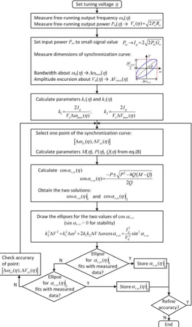
will be calculated through a measurement technique. This will enable an experimental validation of the new envelope-domain formulation that is no subject to errors in the circuit-level description of the standalone oscillator. To facilitate the understanding of thecharacterization procedure, described in the next paragraphs, a flowchart in provided in Fig.1
Fig. 1. Flowchart of the experimental calculation of the oscillator model. Fig. 2 presents the measurement test-bench. An independent signal at the frequency is injected, by means of a circulator, into the same oscillator port used in the practical applications (for spectrum sensing or reading, for instance). Neglecting the circulator insertion loss (considering an insertion loss of 0.5 dB max.), the equivalent input current at the oscillator port will have an amplitude Ig, which should be sufficiently small for the linearization about the free-running solution Vo( ), ( )
o to be valid. Under injection-locked conditions, the circuit equations for each value of the control voltage are given by:( ) ( ) cos( ) ( ) ( ) sin( ) g r r V s o g i i V s o I Y V Y V I Y V Y V (1)
where the superscripts r, i indicate real and imaginary parts, the increments are V V Vo( )
,
o( ) and thedependence of the admittance derivatives with respect to is shown explicitly. Higher-order terms have been neglected and the phase shift between the oscillator voltage V and the input current is –s. Note that the derivatives are directly calculated at the injection port, so there is no need to use additional differentiations with respect to the input source, as in the HB-based method in [13]. Squaring and adding the two terms in (1) the phase shift s disappears and one obtains the equation of an ellipse: 2 2 2 2 2 , 2 0 cos 2 g V V v I Y V Y Y V V Y (2)
where v,ang Y( ) ang Y( )V and the dependence on is not shown for notation simplicity. Solving (1) for , one easily derives that the maximum frequency excursion max of the ellipse (Fig. 1), centered about o, is:
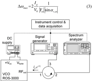
0 , 1 2 sin g max v I V Y (3)
Fig. 2. Experimental setup for the extraction of the oscillator model. The DUT is a Mini-Circuits ROS-3000-819+ Voltage Controlled Oscillator (VCO) (2-3GHz). The external generator signal, for the proposed calculation of the oscillator model, is injected to the oscillator’s output port through a Narda-MITEQ 4923 ferrite circulator.
In turn, solving (1) for V, one derives that the maximum amplitude excursion Vmax of the ellipse, centered about Vo, is: 0 , 1 2 sin g max V v I V V Y (4)
For a given input amplitude Ig, both max and Vmax are easily measurable in the experimental characterization of the oscillator circuit. The free-running oscillation amplitude at the output node is also known, so one can calculate the following quantities, which are functions of the unknown parameters
, V Y Y and sinv, : , 2 ma 1 0 0 x , 2 sin 2 sin V g v max g v k k I Y V I Y V V (5)
Replacing Yv and Y expressed in terms of k1 and k2 in (2), one obtains: 2 2 2 2 2 2 2 1 1 2 , 2 , 0 2 cos g sin v v I V k k k V k V (6)
From a given point
(
e1,
V
e1)
of the experimental ellipse, one can obtain the remaining variable
v,. This is calculated taking into account that sin2v, 1 cos2v,. Replacing this expression into (6) one obtains a second-order equation in,
cos
v, expressed as:
2
, ,
cos v cos v 0
Q P M Q (7)
where the constant coefficients are:
2 2 2 2 2 1 1 1 1 2 1 1 2 2 0 2 e e e e g M V k k k V I Q k P V (8) So cosv, is given by:
2 , 4 2 cos v P P QM Q Q (9)Note that there will be one set of equations (6) to (9) for each . Using a single experimental point
(
e1,
V
e1)
(for each ), there can be two solutions for cos
v,, fulfilling (3) and (4). However, only one of them will be valid. In order to eliminate the unfitting one, one should use a second point of the experimental ellipse(
e2,
V
e2)
. Introducing these new values into (6) and solving (9), one of the two solutions for,
cos
v will remain the same and the other will be different. The value that remains the same is the correct one.Once cos
v,is known, one can directly obtain sinv, and calculate YV , Y from (5). In order to eliminate the sign uncertainty in sin
v,, one should take into account that a necessary condition for the stability of the standalone oscillator is sin
v,0[22]. In practice, several points of the experimental ellipse should be generally considered to reduce the impact of measurement errors (Fig. 1).The procedure for the calculation of the derivatives will be based on (2) to (4), which do not depend on the phase shift s between the oscillator voltage and the input source. This will avoid the need for the two phase-coherent frequency generators, used in [19], as well as the specific arrangements required for the amplitude and phase calibrations of these generators. If wished, a correction of the circulator effects can easily be carried out by considering an incremental admittance term due to mismatch in (1), also making the phase shift s disappear. The calculation procedure is analogous. It is not used here since most of the application examples include this circulator, enabling the observation of the oscillator signal.
With the above procedure it is possible to obtain all the parameters in the linearized oscillator model, except
( )
v ang Yv
. As easily derived from (1) and (2), in the case of injection by independent sources, this angle only constitutes an offset value on the right-hand side of (1), with no implication on the circuit solution. In fact, it can be merged with s to provide a new independent phase value s s v. However,
as will be shown in Section IV, in the self-injection case, the angle
v is needed and can be calculated terminating the oscillator with a known load YL. Its value must be sufficiently close to Yo = 1/50 -1 to enable the oscillator linearization with respect to the termination output admittance, connected in parallel. Thus, the oscillator equation becomes:
+ ( ) + ( ) 0 V L o V L L Y Y V Y Y Y Y V Y Y Y (10)where Y/ YL 1 and YL( )
YL( )
Yo. Splitting (10)into real and imaginary parts and solving for
o( )one obtains: , ( ) sin( ( ) ) | | n ) s ( i L L v v o Y Y (11)
where
L( ) is the angle of YL( )
YL( )
Yo. The aboveequation can be readily solved for
v. As evidenced in Section IV, the two possible solutions of the arcsine function are equally valid. To minimize the errors, measurements of the effect of YL( )
on
o( ) can be carried out in the presence of an injection locking source of very small power to ensure the validity of (2). Then, the free-running frequency can be determined taking into account that, for each , it agrees with the center frequency of the ellipse in (2).The new method is illustrated by means of its application to a commercial oscillator [Mini-Circuits ROS-3000-819+ with:
Pout = 5.5 dBm; tuning voltage range(): 0.5–14 V;
fmin = 2 GHz; fmax = 3 GHz ; and pulling pk-pk @12 dBr = 13.5 MHz]. This oscillator, previously used in [6] for RF identification, will also be considered here for the spectrum-sensing application. For the oscillator characterization, the input power Pin must be sufficiently small to ensure the validity of the linearization in (1), but sufficiently large to enable a clear distinction of the ellipse shape in the presence of measurement errors. Once the correct Pin value has been chosen, a single input-frequency sweep is performed. This should include the synchronization interval existing for Pin. On the other hand, the sweep step f should enable an accurate estimation of the synchronization bandwidth. Here, the value of f = 50 kHz is chosen, providing a reasonable compromise between measurement time and accuracy. For each point of the sweep, the frequency of the injection source and the central frequency of the spectrum analyzer are set to fin n, fin n, 1 . The trace f of the spectrum analyzer is averaged and the output power Pout,n at fin,n is measured. The pair of values fin,n, Pout,n are then used to compute n in n, 0, and Vn Vn V0. This sweep is
automated using the remote control capabilities of the laboratory instrumentation.
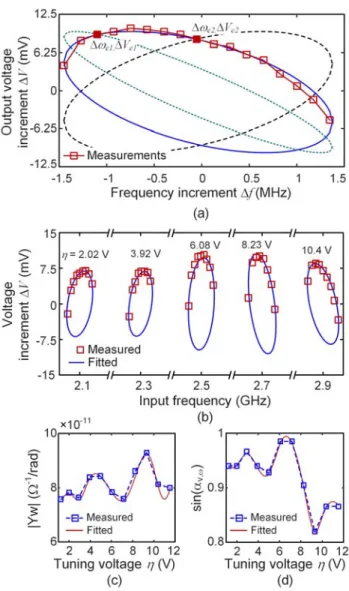
Fig. 3. Experimental oscillator modelling. (a) Comparison of the experimental and fitted ellipse in terms of the oscillation amplitude V versus the frequency
, at the control voltage = 9.3 V. Two points of the experimental ellipse have been considered: (e1,Ve1) and (e2,Ve2). Two ellipses pass through each point, with the same maximum frequency and amplitude excursions
max
and Vmax. However, only one of the two fitted ellipses remains the
same for the two experimental points. (b) Evolution of the measured and fitted ellipses when increasing the control voltage . There is a noticeable variation of the ellipse slant angle, due to the continuous variation of v,. (c) Evolution of Y and (d) sin versus v, .
Fig. 3(a) presents the comparison between the measured ellipse and the ellipse obtained with the new model at the control voltage = 9.3 V, with Pin = -20 dBm. In this representation, two points of the experimental ellipse have been considered, denoted as
(
e1,
V
e1)
and(
e2,
V
e2)
. Two ellipses pass through(
e1,
V
e1)
, traced in solid line and dotted line. These two ellipses have the same maximum frequency and amplitude excursions
max and
V
max,respectively. In an analogous manner, two ellipses pass through
2 2
(
e,
V
e)
, traced in solid line and dashed line. The solid-line ellipse is the same for the two points(
e1,
V
e1)
and2 2
fitted ellipse and the experimental one. Note that only that at the turning points of the ellipse there is a qualitative change of stability. In this case, only the upper section of the ellipse is stable [17], [21] and thus physically observable.
The procedure described enables the calculation of YV,Y
and sin
v, through the sensitivity curve
o( ). Fig. 3(b) shows the evolution of the measured and fitted ellipses when increasing the control voltage . There is a noticeable variation of the ellipse slant angle, due to the continuous variation of, .
v
The derivatives obtained for different values should be properly interpolated. The variations of Y and sin
v, versus , obtained in this particular case, are shown in Fig. 3(c) and Fig. 3(d). If either the variations of these parameters or the excursion in are small, it will be possible to approximate the oscillator frequency characteristic with the expression( )
oo KV o
, where KV is the slope of the frequency characteristic at a central point o, oo.III. EXTERNALLY INJECTED CHIRPED OSCILLATOR In this section, a chirped oscillator injected by several independent signals fk, as shown in Fig. 4, is considered. Instead of a circuit-level envelope-domain formulation [23]-[26], a two scale semi-analytical formulation, relying on the oscillator model of Section II, is presented. The use of two time scales allows handling the different time rates associated with the chirp signal and the beat frequency. In comparison with [13], this formulation is not based on the assumption of a linear frequency characteristic of the voltage-controlled oscillator. Instead, this characteristic is represented with the general function
o( ). In a second stage, noise perturbations will be introduced into the formulation. Then, the carrier-detection capabilities under dynamic synchronization and using the variation of the beat frequency are analyzed.A. System formulation
For the system formulation, one will assume that a sawtooth waveform is introduced at the oscillator control-voltage node. In the absence of input signals, this gives rise to an instantaneous oscillation frequency o
( )t
. Now, it is assumed that one or more signals are injected into the oscillator-analysis port [1]-[2], which are represented with the input current source i t( ):
1 ( ) ( ) Re ( ) , () exp , ( ) Δ o N j k k k k k t k o U t i t U t e I j t
(12) where , , , 1, … , , are the amplitude, phase and frequency of each input signal and o
( )t
has been taken as the carrier frequency. The first-harmonic component of the voltage at the observation node, X t1( ), is expressed as:( )
1( ) ( ) j t , () o( ) Δ ( )
X t V t e V t V V t (13)
This component can be related to U in (12) through the outer-tier admittance function Y, which derives from the application of the Implicit Function Theorem to the HB system [17]. When applied to the time-varying complex envelope X1(t), the frequency dependence of the function Y leads to a differential equation, as shown next. The relationship between X1(t) and
U(t) is initially expressed with the following time-frequency
equation [17],[22]:
( )
1 ( ), / ( ) e ) xp ) , Δ ( ( N j t k k k k o k o k Y V t s j V t e I j t
(14) where s is a time differentiator, which arises due to the time-varying nature of the voltage signal in (14) [17],[22]. The frequency increment ( )t resulting from this time differentiation will be small, since the input frequencies are close to o
( )t
. Taking also into account the smallamplitude increment in the presence of low power input signals, a first-order Taylor series expansion about Vo
( )t
and
( )
o t
can be carried out in (14), which leads to:
1 Δ Δ Δ ( ) ( ) ( ) ( ) exp o V o N k k k k V Y V Y j V V I j t t V V
(15) where higher-order terms have been neglected. The dynamic linearization of the admittance function about each free-running frequency
o( ) ensures a small magnitude of the frequency perturbation term . This is because the effect of the frequency increments
k is limited by the complex exponential. Thus, (15) enables a high level of accuracy. Neglecting the time-varying term ∆ in (15), splitting into real and imaginary parts and solving for one obtains:
1 , sin sin N k k k k o v v I t Y V
(16)Note that the angle
v of the voltage-amplitude derivative is just an offset value, which can be absorbed in the variable . From the inspection of (16), to maximize the sensitivity to the external signals, one should minimize Ysinv,, which can be achieved by reducing the oscillator quality factor.To get more insight into the formulation, the case of a single input signal with frequency 1 will initially be considered. In this case, and in the absence of a chirp modulation (considering a constant ), (16) models an injection-locked oscillator, whose steady-state solution has been analyzed in detail in previous works [29]-[30]. One obtains:
' ( ) kexp b , off o( ) o( ) k off t t P jk t
(17)where o'( ) is the free-running oscillator frequency pulled by
the input signal and b o' 1 is the beat frequency. The harmonic components Pk are responsible for the presence of beat tones in the unlocked oscillator spectrum, at the harmonics of the beat frequency k
b. In the sensing application, the amplitude of the input signals must be small enough for the linearization about the free-running solution to be valid, so a number NH=5 of harmonic terms should be suitable.If the sawtooth control voltage (t) is now considered, there will be two different time scales in the system: one associated with to the slow varying (t), in the order of kHz, and the other one associated with the beat frequency
b( )t , in the order of tens of MHz. For computational efficiency, the extension of (17) to the case of a slowly-varying control voltage (t) will be performed using two time scales:
1 2 1 2 1 2 1 1 2 ' 1 1 1 ˆ , , ˆ , ( ) ( ) exp ( ) , ( ) ( ) ( ), off b NH k off k NH o o t t t t t t t P t jk t t t t t
(18) The slow time scale t1 is associated with the time-varyingtuning voltage and gives rise to a slow time variation of the free-running and pulled frequencies, given by
1 1 ( ) ( ) o t o t , ' '
1 1 ( ) ( ) o t o t , respectively. Thus, the beat frequency is now b( )t1 o'( )t1 1. The harmonic components in expression (18) also vary at the slow time scale
1
t . On the other hand, the faster scale t2 is due to the presence of the beat frequency
b( )t1 . Taking into account the double dependence on the two time scales, the time derivative ( )t in(16) is obtained as:
1 2 1 2 1 2 1 1 2 1 1 1 1 2 1 2 ˆ , ˆ , ˆ , ( ) exp , NH b k b o k NH ff t t t t t t t t t t t jk t P t jk t t t t t
(19) The introduction of (19) into (16), provides an envelope-transient formulation of the system at the fundamental frequency b
t1 , which is also an unknown of the problem.In Sections III-C and III-D two cases will be distinguished: an input power such that the oscillator gets locked to the input signal during a fraction of the chirp period, and an input power below the locking threshold, though still enabling the detection of the input signal from the dynamics of the beat frequency.
B. Noise analysis
The noise contributions of the standalone oscillator are modeled with the fitting method proposed in [27], though here it is applied experimentally. In this method a single noise source at the output port is considered, fitting its spectral density so that the phase-noise spectrum resulting from the semi-analytical formulation matches the reference one. This can be obtained
from a circuit-level simulation with multiple noise sources, using the conversion-matrix approach, as in [27], or, from an experimental measurement, as in this work. As derived in [27], this phase-noise spectrum is given by:
2 2 2 2 2 2 2 2 2 , 2 2 , 2 ( , ) ( ) ( ) ( ) ( , ) ( ) ( sin s ) in ( ) F w o N v v o K I V I Y Y V (20)
where Iw is the equivalent white-noise current (including
input noise) at the oscillator analysis port, the coefficient KF is a proportionality constant, accounting for the effect of the flicker noise, and IN is the total equivalent noise current. Note
that the admittance-function derivatives, calculated at
( ), ( )
o o
V
, change with . The spectral density IN( , ) 2is obtained by fitting the measured phase-noise spectrum with the expression (20). This source is introduced into (15), which governs the injected-oscillator behavior:
1 ( ) ( ) ( ) Δ exp ( ), V N k k k N o k Y V Y I j t I t V
(21)where IN( )t IN( , ( ))t
t is the stochastic process whose power spectral density (PSD) is IN( , )
. Splitting (21) into real and imaginary parts and solving for , one obtains:
1 , ( ) ( ) ( sin sin ) ( ) N k k k v k o v t V I t Y
(22)where the noise term
( )t is given by:
( ) ( ) ( ) ( )
( ) ( ) ( ) ( ) ( ) ( ) r i i r V NT V N i r V V o T r i Y I t Y I t t Y Y Y Y V (23)Note that
( )t is a stochastic process whose statistical properties vary periodically with the chirp signal
( )t . When including the effect of colored noise sources in IN( )t , this process may become non-stationary. As derived in [28], if the measuring time interval is short enough, IN( )t can be approached by a stationary process in this interval. In that case,( )t
will be cyclostationary.The nonlinear stochastic differential equation (SDE) (22) is solved through linearization about the unperturbed solution
0( )t
of (16), previously calculated by the bivariate technique of Section III.A. The noise term introduces a small phase perturbation of the form
0( )t
( )t that can be calculated by approaching the nonlinear term in (22) by its first-order Taylor expansion and cancelling the steady-state components:
0
1 i , ( ) ( c ( ) ( ) os ( ) n ) s N k k k v k o v I t t Y t V
(24)The linear time variant (LTV) equation (24) is solved through direct integration. Different realizations of
( )t may be considered, according to the spectral density of the noise sources. The term
( )t will enable the analysis of the impact of noise perturbations on the dynamic synchronization intervals and the minimum detectable signal.C. Instantaneous injection locking
For input power above a certain threshold, the chirped oscillator will become injection locked for one or more time intervals of the chirp-signal period, depending on the number of input signals and their frequency and power values. Initially, the case of a single input signal is considered. The partial derivative with respect to t1 can be neglected in (19), since
1 ( ) off t
, b( )t1 and P tk( )1 are slowly-varying components.
Then, outside the locking intervals, (19) predicts that, at each t1
, the time derivative ( )t is a periodic signal centered atoff( )t1 , with period T tb( )1 2 / b( )t1 .
On the other hand, within the locked interval, one has
1 1 1 1 2 1 1 2 1 ( ) ( ( )) ( ) 0 ( ( )) ( ( )) , off i o b i o t t t t t t t t t t t t t (25) where
( ( ))t1 is the slow phase shift resulting from the time variation of . Replacing into the general expression for the voltage signal one has:
( ) ( )
( )
( ) Re ( ) j t jo t Re ( ) j t j ti o
v t V t e e VV t e e (26)
Then, from (26), the instantaneous frequency becomes
( )t
i
, predicting a single-tone spectrum at
i. In the case of a single input carrier at
1, one will have
( )t
1. With two (or more) input carriers, the instantaneous frequency will vary in a nearly periodic (or quasi-periodic) manner within the synchronization intervals, which is due to the mixing with the other input frequencies.
1 1 , , 1 1 2 1 2 , , 1 ( ) m( ) exp , m m k k m k k t Q t j k k t t t t
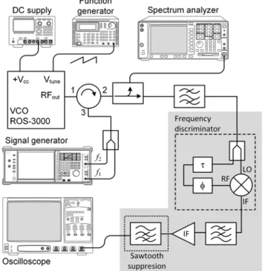
(27)The analysis method has been applied to the oscillator in Fig. 2. As shown in the setup of Fig. 4, the oscillator is connected to a frequency discriminator to demodulate the frequency variations. The delay and phase shift of the mixer-based frequency discriminator are adjusted so that, in the absence of external excitations (f1 and f2 in Fig. 4), the signal at the oscilloscope corresponds to the one provided by the function generator. After this demodulation, a high-pass filter is used in some cases to suppress the voltage ramp due to the sawtooth signal. Note that the frequency can also be demodulated detecting the bias current or voltage drop in a
resistor introduced in the bias line [6], as will be done in Section IV.
Fig. 4. Setup for the experimental characterization of the chirped oscillator in the presence of independent input excitations. The external excitation signals, from an Anritsu MG3710A signal generator, are combined and injected to the oscillator using a Narda 4923 circulator. The oscillator is connected to a mixer-based (Marki ML1-0113) frequency discriminator to demodulate the frequency variations. After demodulation, a high-pass filter will also be used in some cases to suppress the voltage ramp due to the sawtooth signal. A spectrum analyzer was connected through a directional coupler only for spectrum monitoring. A Keysight Infiniium 90804A Digital Storage Oscilloscope is used to measure the demodulated output.
In the first analysis, a sawtooth control voltage at 1 kHz, in the presence of one independent signal at f1 = 2.48 GHz with the power Pin = 27 dBm has been considered. Fig. 5 presents the time variations of the output voltage of the frequency discriminator during a period of the sawtooth signal. The results of (22) are compared with the experimental measurements, observing a very good agreement. Note that these results are obtained with the chirped oscillator only, without any prior amplification of the input signal. The output voltage of the frequency discriminator flattens in the dynamic synchronization interval, as predicted by (25). This interval is approximately centered about the time point at which the sawtooth signal takes the value required by the standalone oscillator to oscillate at f1 = 2.48 GHz. Both the synchronization time interval and the variations of the beat frequency outside this interval are well predicted by the formulation. As derived from (18), the beat frequency grows when moving away from the limits of the dynamic synchronization interval. The peaks point downwards (upwards) when the self-oscillation frequency is higher (lower) than the input frequency. It is worth mentioning that, as shown in [13], it is not possible to perform any circuit-level envelope-domain simulation at 1 kHz. This is due to an excessive computational cost, since the envelope sampling must account for the highest beat frequency during
the sawtooth signal period, which leads to an unbearable number of data points.
As observed in Fig. 5, the experimental noise perturbations are stronger than the simulated ones, since the former include numerical noise associated with the sampling. Both in measurement and simulation, the noise effects are less pronounced at the center of the synchronization interval, where the influence of the input signal over the oscillator behavior is stronger.
Fig. 5. Time variations of the output voltage of the frequency discriminator during a period of the sawtooth signal at 1 kHz. Results of (22) are compared with the experimental measurements in the presence of one independent signal at f1 = 2.48 GHz with the power Pin = 27 dBm. Note that these results are
obtained with the chirped oscillator only, without any prior amplification of the input signal.
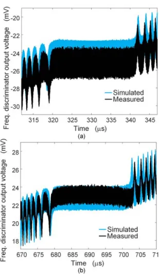
Fig. 6 compares the results of (22) with experimental measurements, under a chirp signal of 1 kHz, in the presence of two inputs at f1 = 2.49 GHz and f2 = 2.51 GHz, with the same power Pin = 27 dBm. As in the case of Fig. 5, no high-pass filter has been connected to the output of the frequency discriminator, so the impact of the ramp signal can be noted. During the chirp signal period, the circuit first gets locked to f1 and then to f2. In each of the two intervals of dynamic synchronization, at f1 and f2, the output of the frequency discriminator exhibits time variations associated with the mixing with f2 and f1, respectively. This is why the voltage excursions are larger than in Fig. 4. Nevertheless, the two input signals are clearly detected.
Fig. 7(a) and Fig. 7(b) present expanded views of the output voltage of the frequency discriminator about the two dynamic synchronization intervals. In the two cases there is an excellent prediction of both these intervals, with a flattened voltage variation, and the distinct voltage variations under unlocked conditions, with pronounced downward and upward peaks of growing frequency.
Fig. 6. Output voltage of the frequency discriminator during one period of the sawtooth signal at 1 kHz, in the presence of two inputs at f1 = 2.49 GHz and f2 = 2.51 GHz, with the power Pin = 27 dBm. The results of (22) are compared with
experimental measurements.
Fig. 7. Expanded views of the output voltage of the frequency discriminator about the two dynamic synchronization intervals. In these two time intervals the sawtooth signal is about the tuning voltages corresponding to f1 and f2, respectively. (a) Dynamic synchronization interval about f1 = 2.49 GHz. (b) Dynamic synchronization interval about f2 = 2.51 GHz.
D. Detection from the beat frequency
The two boundaries of each synchronization interval correspond to the time values at which the beat frequency
i
decreases to zero and grows from zero, respectively [13]. The mathematical condition for this dynamic bifurcation can be expressed as
t , where is a threshold used for thenumerical detection. When progressively reducing the input current, a value should be reached Igmin at which the two time points merge in a single one tc, where i o
( )tc
. With input current below Igmin, detecting an input signal is still possible, taking into account the impact of this signal on the sign of the beat frequency. In order to understand this phenomenon, initially, the case of a single input signal is considered. For I1 <Igmin, the frequency pulling can be neglected due to the small amplitude of I1, so the beat frequency can be approached as:1 1
( )t i 0, t I t( ) [c tc t t,c
t]
(28)where I t( )c is the small time interval for which the condition 1
( )t i 0
is fulfilled . The presence of several input signals will modulate the signal
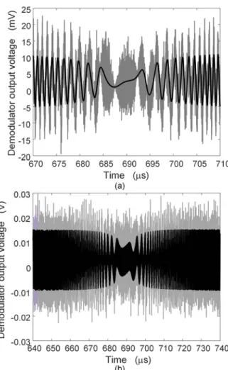
( )t . However, provided the input power is not too low, the significant slowdown of the dynamics in the neighborhood of each input frequency will still enable the frequency detection.Fig. 8 shows the simulated and measured signal in the presence of two input carriers. This is obtained after passing through the frequency discriminator and the high-pass filter, shown in the setup of Fig. 4. Two input carriers are considered, with the power Pin 41 dBm at the respective frequencies f1 = 2.49 GHz and f2 = 2.51 GHz. As in the previous case, the input carriers are directly introduced into the oscillator, without any previous amplification stage. Fig. 8(a) [Fig. 8(b)] presents an expanded view in the time interval for which the sawtooth signal is about the tuning voltage corresponding to f1 = 2.49 GHz (f2 = 2.51 GHz).
Fig. 8. Demodulator output voltage in the presence of two input signals f1 = 2.49 GHz and f2 = 2.51 GHz with an input power Pin = 41 dBm, below the one
required to reach any locked states. Simulation results are compared with experimental measurements in the time interval for which the sawtooth signal is about the tuning voltage corresponding to f1 = 2.49 GHz.
The introduction of a noise term enables an investigation of the impact of the noise perturbations on the minimum
detectable signal, which should depend on the number of input carriers. Fig. 9(a) compares the time variations of the output voltage of the high-pass filter in Fig. 4 with and without noise perturbations, in the presence of a single input carrier at
f1 = 2.49 GHz. The input power considered is Pin = 51 dBm. The noisy signal is represented with a light trace. Fig. 9(b) shows the same comparison in the presence of two input carriers at f1 = 2.49 GHz and f2 = 2.51 GHz, with Pin = 51 dBm. As expected, a higher input power is required for the detection of two carriers, which is due to the mixing effects.
IV. SELF-INJECTED CHIRPED OSCILLATOR
The recent work [6] demonstrates the application of a chirped oscillator as a low-cost reader for chipless RF identification. In [6], this reader oscillator is connected to a horn antenna, which transmits the oscillator signal and receives the signal reflected by a backscatter tag. The resonance signature of the tag affects the oscillator instantaneous frequency due to pulling effects. This can also be interpreted as the result of the self-injection locking of the oscillator circuit by the reflected signal. As experimentally demonstrated in [6], the bit signature of the tag can be recovered from the instantaneous variation of the oscillator bias current (or voltage drop in a bias resistor), which changes with the oscillation frequency and operation conditions. Through this mechanism, the tag signature can be easily extracted through signal processing, which avoids the need for an expensive receiver front-end.
The focus of this section is the envelope-domain formulation of the chirped oscillator in self-injection locked regime. The oscillator receives its own signal affected by the propagation effects and the tag frequency signature. In these conditions, the oscillator output is loaded with an the equivalent reflection
( )
L
of small magnitude (due to the propagation effects), instead of 50 . This coefficient can be transformed into an equivalent admittance by doing:
1 ( ) ( ) 1 ( ) L L o L Y Y (29)
Since L( )
has a low magnitude, the admittance YL( )
will be close to the original load admittance Yo = 1/50 -1. Thus, one can linearize the oscillator admittance function Y with respect to the load admittance connected in parallel at the output node, which provides the following additional small term:( ) ( )
L L o
Y
Y
YFig. 9. Analysis of the influence of noise perturbations on the minimum detectable signal for the cases of one and two input carriers. Comparison of the time variations of the output voltage of the high-pass filter connected to the output of the frequency discriminator with and without noise perturbations. The light trace corresponds to the noisy simulations. (a) In the presence of a single input carrier at f1 = 2.49 GHz. The input power considered is Pin = 51 dBm.
(b) In the presence of two input carriers at f1 = 2.49 GHz and f2 = 2.51 GHz. The input power considered is Pin = 51 dBm.
In order to introduce this additional function in the envelope-domain equation, its low-pass equivalent is calculated as:
, ( , ) ( ( ) )
L lp L o
Y
Y
(31)
Then, the self-injected oscillator is governed by the following integro-differential equation:
, 1 1 ( ) 1 ( ) ( ) ( ) ( ) ( ) = ( ) ( ) ( ) ( ) = , ( ) ( ) ( ) ( ) V o L lp j t o V t Y V t Y t j V V t y t X t X t X t V V t e (32) where yL lp, ( )t is the low-pass impulse response associated with YL lp, ( ) . Note that left side of (32) is analogous to the left side of (15). The key difference is on the right side, which in (15) corresponds to independent excitation signals and in (32) accounts for a reflected signal, affected by the propagation and tag resonance effects. In the two cases, the independentvariables of (32) are the phase
( )t and amplitude V t( ). The equation governing the phase dynamics can be decoupled from (32) by neglecting V t( ) 0 , which is a reasonable approach since the reflected component only perturbs slightly the oscillator amplitude. Under the assumption V t( ) 0 one obtains: ( ) , 1 ( ) ( ), ( ) ( ) ( ) , ( ) ( ) ( ) ( ) ( ) ( ) j t lp V lp L lp o V t c t i t e Y c t i t y t X t V Y Y (33) Equation (33) shows that the phase variable
( )t can be expressed in the form (18). It is relevant to indicate that under an unrealistic linear model of the oscillator frequency characteristic, the frequency deviations with respect to this idealized variation may hide the smaller pulling effects. In general, this linear characteristic is more difficult to maintain when the chirped oscillator covers a broad frequency band. Thus, the usefulness of considering a general expression
( )
o t
. In the case of (33), the slow time scale t1 is associated with the time-varying tuning voltage
( )t and the fast time scale t2 is associated with the frequency shift , due to pulling effects. Since the reflected term produces a small perturbation, this pulling will be considered in the oscillation frequency only, neglecting second-order effects described by the harmonic components P tk( )1 in (18). Setting these components to zero, the phase equation (33) can be rewritten in terms of bi-variate functions as:
1 2 1 2 2 ( ) 2 1 2 1 1 1 ( ) 2 , 1 1 1 1 1 2 1 2 1 1 1 ˆ( , ), ˆ ( , ) ( ( )) ˆ( , ) , ( ) ˆ( , ) ( ( )) ( ( )) ( ( )) ˆ ( , ) ( ), ˆ , ( ) ( ( ˆ , ˆ ( )) , ( ) , , ) ( j t lp V o V j t lp L lp o lp p t t l c i t e Y t c c t c V t Y t Y t i Y t t V t e i t i t t t t t t t t t t t t t t t t t t t t t t
2 ) ˆ ,tt t (34)where a b Re( )Im( ) Im( )Re( )a b a b . Then, neglecting the time derivative with respect to the slow time scale t1, the instantaneous frequency ( )t1 at each value of t1 can be obtained from the equation:
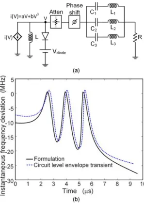
, 1 1 1 1 1 1 , 1 ( ), ( ) sin ( ( ) ( ( ))) ( ) ( ( )) ( ( )) | | sin p v L l t t L t v t t Y t t Y (35)The above semi-analytical formulation has initially been validated through a comparison with envelope-domain simulations at circuit level. A simple oscillator based on a cubic nonlinearity has been considered, shown in Fig. 10(a). The oscillation frequency is varied with a sawtooth-voltage signal (t), introduced into a varactor diode. The circuit is loaded with an attenuator and a phase shifter, emulating the propagation
effects, and three series resonators connected in parallel, at the frequencies 2.35 GHz, 2.5 GHz and 2.65 GHz, comprised within the oscillation-frequency interval due to (t). The instantaneous frequency deviation obtained with the new formulation and with circuit-level simulations is shown in Fig. 10(b). As can be seen, there is a very good agreement.
Fig. 10. Validation of the semi-analytical formulation under self-injection locked conditions through circuit-level envelope-transient simulations. (a) Simple oscillator based on a cubic nonlinearity. The oscillation frequency is varied with a sawtooth-voltage signal (t), introduced into a varactor diode. The circuit is loaded with an attenuator and a phase shifter, emulating the propagation effects, and three series resonators connected in parallel, at the frequencies 2.35 GHz, 2.5 GHz and 2.65 GHz, comprised within the oscillation-frequency interval due to (t). (b) Comparison of the instantaneous frequency deviation ( )t1 obtained with the new formulation and with circuit-level
simulations.
In the radiofrequency identification example, two different types of tags are considered, based on retransmission [20] and on backscatter [7]. For a detection of the tag bit pattern, the sawtooth control voltage of the chirped oscillator must be able to cover the whole frequency interval of the chip resonances [6]. Then, the instantaneous frequency will exhibit a distinct time variation, depending on the tag resonance signature.
In the case of a retransmission tag, shown in the setup of Fig. 11(a), the oscillator output is connected to Port 1 of a circulator and, in order to isolate the transmitted and received signal, antennas with orthogonal polarization are connected to Port 2 and Port 3 of this circulator. The oscillator signal is transmitted with a horizontally polarized antenna, connected to Port 2. At a close distance, there is a tag with a horizontally polarized receiving antenna. The retransmission tag, shown in Fig. 11(b), has been implemented following [20] and may contain several coplanar waveguide spiral resonators, each corresponding to a coding bit. The tag output is connected to a transmitter antenna that is vertically polarized. This signal is received by a
vertically polarized antenna, connected to Port 3 of the circulator. The increment in the output admittance YL lp, ( ) accounts for the tag resonance signature, as well as the propagation effects. As clearly shown by (35), the resonances in YL lp, ( ) will affect the instantaneous frequency ( )t1 . Thus, as predicted by [6], one should be able to read the tag resonance signature from the oscillator instantaneous frequency or, equivalently, from the variation of the bias-line current or voltage drop in a resistor introduced in this bias line.
Since the focus of this work is the oscillator performance, instead of the modelling of propagation plus tag resonance effects, the function YL lp, ( ) has been obtained from an experimental measurement of the input reflection-coefficient
( )
L
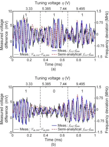
at Port 1 of the circulator. Fig. 12 compares the differences in the instantaneous frequency for various resonance signatures, obtained through the semi-analytical formulation and experimentally. The instantaneous frequency differences for two cases (‘101’ and ‘111’), normalized using the reference ‘000’, have been represented versus the time-varying control voltage . Fig. 12(a) compares the simulated and measured differences in the instantaneous frequency when using the signature reference ‘000’ and the signature ‘111’. The measured difference of the voltages Vdc,111 and Vdc,000 is also represented. Fig. 12(b) compares the differences when using the signature ‘101’ and the signature ‘000’. As can be seen, there is a very good agreement. Discrepancies are mostly attributed to the oscillator frequency drift, since the overall system operates in a free-running regime. The measured voltage difference (Vdc,101-Vdc,000) has also been represented. The more pronounced variations at the higher values are due to the lower magnitude of the function s ni
v,( ), as gathered from (35) and the variations of s ni
v,( )shown in Fig. 3(d).The case of a backscatter tag [7] has also been considered. In this case, sketched in Fig. 13(a), the oscillator is directly connected to an antenna, with no need for a circulator. The same antenna transmits the oscillator signal and receives the signal reflected by the tag. The backscatter tag consists of a series of C-shaped resonators, as proposed in [7]. Fig. 13(b) compares the simulated and measured differences in the instantaneous frequency when using the signature ‘011’ and the signature reference signature ‘000’. The measured voltage difference (Vdc,011-Vdc,000), which agrees with the instantaneous frequency variations, has also been represented. As can be seen, there is a very good agreement between the measurements and the prediction.
Fig. 11. Self-injected chirped oscillator. (a) Setup for a retransmission tag, connecting the oscillator output port to Port 1 of a circulator. The transmitting and receiving antennas, with orthogonal polarization, are connected to Port 2 and Port 3 of the circulator, respectively. The test fixture, including a series resistor in the bias line, allows the measurement to the bias voltage variations due L(). The VCO frequency, voltage and current (in static conditions) are
measured by means of a directional coupler, connected to a spectrum analyzer, and digital multimeters, respectively. A TG1010A DDS function generator, provides a sawtooth signal with the voltage excursion, required by the ROS-3000-819+ VCO, to cover the 2GHz-3GHz band. (b) Photograph of the retransmission tag with two orthogonally polarized antennas (R&S HL050). The tag contains coplanar waveguide spiral resonators and is implemented in RO4003C substrate.
Fig. 12. Comparison of the differences in the instantaneous frequency for difference resonance signatures, obtained through the semi-analytical formulation and experimentally. (a) Simulated and measured differences in the instantaneous frequency when using the signature 111 and the signature 000. The measured voltage difference (Vdc,111-Vdc,000) has also been represented (b)
Simulated and measured differences when using the signature 101 and the signature 000. The measured voltage difference (Vdc,101-Vdc,000) has also been
represented.
V. CONCLUSIONS
An envelope-domain formulation for an accurate analysis of injected and self-injection locked chirped oscillators has been presented. The new formulation considers a general dependence of the free-running oscillation frequency on the control voltage, which enables its application to oscillators with a tuning characteristic that deviates from a linear one. It relies on a realistic model of the standalone oscillator, which can be extracted through circuit-level harmonic-balance simulations or experimentally. Here an experimental technique has been presented, based on the fitting of the synchronization curves obtained for different tuning voltages. The experimental oscillator model allows a consistent validation of the new formulations without uncertainties due to modeling inaccuracies in the passive and active components of the oscillator circuit. Chirped oscillators injected by independent signals, as in spectrum sensing applications, are formulated in the envelope domain, with a slow time scale, corresponding to the slow chirp frequency, and a faster time scale, corresponding to the beat frequency. Both the dynamic synchronization intervals and the instantaneous frequency variations outside these intervals are accurately predicted. Noise perturbations are introduced in the form of an equivalent current source at the
injection port, which enables the determination of the minimum detectable signal in the presence of one or more input carriers. The envelope-domain formulation has also been used to investigate the self-injection-locked operation of the chirped oscillator, recently proposed for low-cost readers in radiofrequency identification. This formulation enables an insightful prediction of the effect of the tag resonance signature on the instantaneous oscillation frequency.
Fig. 13. Oscillator performance when using a backscatter tag. (a) Setup for a backscatter tag by directly connecting the oscillator output port to an antenna. The tag is the similar to the one proposed in [7] and used in [6]. The VCO frequency, voltage and current (in static conditions) are measured through the RF port of the bias-tee (leakage) and digital multimeters, respectively. (b) Simulated and measured differences in the instantaneous frequency when using the signature ‘011’ and the reference signature ‘000’. The measured voltage difference (Vdc,011-Vdc,000) has also been represented.
REFERENCES
[1] F. K. Wang et al., "An injection-locked detector for concurrent spectrum and vital sign sensing," IEEE MTT-S Int. Microw. Symp., Anaheim, CA, 2010, pp. 768-771.
[2] C. J. Li, F. K. Wang, T. S. Horng and K. C. Peng, "A Novel RF Sensing Circuit Using Injection Locking and Frequency Demodulation for
Cognitive Radio Applications," IEEE Trans. Microw. Theory Techn., vol. 57, no. 12, pp. 3143-3152, Dec. 2009.
[3] L. Larson, S. Abdelhalem, C. Thomas and P. Gudem, "High-Performance Silicon-Based RF Front-End Design Techniques for Adaptive and Cognitive Radios," IEEE Comp. Semicond. Integr. Circuit Symp.
(CSICS), La Jolla, CA, 2012, pp. 1-4.
[4] E. E. Djoumessi and K. Wu, "Reconfigurable RF front-end for frequency-agile direct conversion receivers and cognitive radio system applications," IEEE Radio and Wireless Symp. (RWS), New Orleans, LA, 2010, pp. 272-275.
[5] A. Mayer et al., "RF Front-End Architecture for Cognitive Radios," 2007
IEEE Int. Symp. Pers. Indoor Mob. Radio Comm., Athens, 2007, pp. 1-5.
[6] N. B. Buchanan and V. Fusco, "Single VCO chipless RFID near-field reader," Elect. Lett., vol. 52, no. 23, pp. 1958-1960, 11 10 2016. [7] A. Vena, E. Perret and S. Tedjini, "A Fully Printable Chipless RFID Tag
with Detuning Correction Technique," IEEE Microw. Wireless Comp.
Lett., vol. 22, no. 4, pp. 209-211, April 2012.
[8] S. Preradovic, I. Balbin, N. C. Karmakar and G. F. Swiegers, "Multiresonator-Based Chipless RFID System for Low-Cost Item Tracking," IEEE Trans. Microw. Theory Techn., vol. 57, no. 5, pp. 1411-1419, May 2009.
[9] M. A. Islam and N. C. Karmakar, "Compact Printable Chipless RFID Systems," IEEE Trans. Microw. Theory Techn., vol. 63, no. 11, pp. 3785-3793, Nov. 2015.
[10] M. Pontón and A. Suárez, "Wireless Injection Locking of Oscillator Circuits," IEEE Trans. Microw. Theory Techn., vol. 64, no. 12, pp. 4646-4659, Dec. 2016.
[11] S. Preradovic and N. C. Karmakar, "Design of fully printable planar chipless RFID transponder with 35-bit data capacity," Eur. Microw. Conf.
(EuMC), Rome, 2009, pp. 013-016.
[12] N. Karmakar, P. Kalansuriya, R. Azim, and R. Koswatta, Chipless Radio
Frequency Identification Reader Signal Processing, John Wiley & Sons,
Hoboken, 2016.
[13] F. Ramírez, S. Sancho, M. Pontón, and A. Suárez, “Analysis of chirped oscillators under injection signals,” IEEE MTT-S Int. Microw. Symp., Philadelphia, Jun. 2018.
[14] F. Ramírez, M. Pontón, S. Sancho, A. Suárez, “Stability analysis of oscillation modes in quadruple-push and Rucker’s oscillators,” IEEE
Trans. Microw. Theory Techn., vol. 56, no. 11, pp. 2648-2661, Nov., 2008.
[15] A. Suárez, F. Ramírez, and S. Sancho, “Stability and Noise Analysis of Coupled-Oscillator Systems,” IEEE Trans. Microw. Theory Techn., vol. 59, no. 4, pp. 1032-1046, Apr. 2011.
[16] S. Sancho, M. Ponton, and A. Suarez, "Nonlinear technique for the analysis of the free-running oscillator phase noise in presence of an interference signal," IEEE MTT-S Int. Microw. Symp., Honololu, HI, 2017, pp. 79-82. [17] A. Suarez, Analysis and Design of Autonomous Microwave Circuits,
Wiley, Hoboken, New Jersey, 2009.
[18] S. Sancho, F. Ramírez, and A. Suárez, "Stochastic Analysis of Cycle Slips in Injection-Locked Oscillators and Analog Frequency Dividers," IEEE
Trans. Microw. Theory Techn., vol. 62, pp. 3318-3332, 2014.
[19] P. Umpierrez, V. Arana, and F. Ramirez, "Experimental Characterization of Oscillator Circuits for Reduced-Order Models," IEEE Trans. Microw.
Theory Techn., vol. 60, no. 11, pp. 3527-3541, Nov. 2012.
[20] S. Preradovic and N. C. Karmakar, "Chipless RFID: Bar Code of the Future," IEEE Microw. Mag., vol. 11, no. 7, pp. 87-97, Dec. 2010. [21] A. Suárez and R. Melville, "Simulation-assisted design and analysis of
varactor-based frequency multipliers and dividers," IEEE Trans. Microw.
Theory Techn., vol. 54, pp. 1166-1179, Mar., 2006.
[22] K. Kurokawa, "Some basic characteristics of broadband negative resistance oscillators," Bell Syst. Tech. J., vol. 48, no. 6, pp. 1937-1955, Jul. –Aug. 1969.
[23] E. Ngoya and R. Larcheveque, "Envelope Transient Analysis: A New Method for the Transient and Steady State Analysis of Microwave Communication Circuits and Systems," IEEE MTT-S Int. Microw. Symp., San Francisco, CA, June 1996, pp. 1029-1032.
[24] H.G. Brachtendorf, G. Welsch, R. Laur, and A. Bunse-Gerstner, “Numerical steady state analysis of electronic circuits driven by multi-tone signals.” Electronic Engineering, Vol. 79, pp. 103-1 12, 1996.