PIPELINE-BASED POWER REDUCTION IN FPGA APPLICATIONS
Miguel A. Sacristán, Victoria Rodellar
*DATSI – Facultad de Informática
Universidad Politécnica de Madrid
Campus de Montegancedo S/N
28660 - Boadilla del Monte (SPAIN)
email: [email protected],
[email protected]
Antonio Díaz
*ATC – Escuela de Informática
Universidad Politécnica de Madrid
Ctra. Valencia Km. 7
28031 – Madrid (SPAIN)
email: [email protected]
ABSTRACT
This paper shows how temporal parallelism has an important role in the power dissipation reduction in the FPGA field. Glitches propagation is blocked by the flip-flops or registers in the pipeline. Several multiplication structures are implemented over modern FPGAs, StratixII and Virtex4, comparing their results with and without pipeline and hardware duplication.
1.INTRODUCTION
Portability is a very important topic in today applications even more in DSP field. Power consumption reduction is useful not only for extending the life of the batteries but for downsizing the heat dissipation mechanisms.
Design for Low Power, DfLP, can be applied to all the levels of the design.; approaches at the system level include the reduction of the power supply [1], disconnection of the system clock (gating clock) [1], low power operation modes [2] and managing which parts of the system must stay activated in each moment [3]. Algorithmic methods contain the use of alternative numeric systems [4], codification of the state machines, optimization of the memory accesses [5] and decrease of the number of transitions in each net of the circuit [6]; circuit level techniques comprise asynchronous implementations of self temporized circuits and glitches reduction [7]; transistor rearrangement [8] at physical level; and, finally, technology level [9] makes use of different implementations like dynamic threshold transistors MOSFET(DTMOS) [10].
At the same time, FPGA devices are becoming very important in the rapid prototyping methodology for DSP with high level synthesis. Last generation devices include specific circuitry to implement the DSP basic operations,
like addition, multiplication and inner product (multiplication with accumulation). But, in this case, technology of implementation, power supply, transistor arrangement and signal temporization are fixed by the chosen FPGA. Moreover, all these parameters are not accessible in a high level synthesis environment because of its technology independence. So power dissipation reduction through parallelism increasing, as a high level affordable technique, is going to be tested over a typical DSP operation, multiplication. Pipelining [11][12], temporal parallelism, inserting pipeline registers, reduces glitch transmission in a FPGA.
2.MULTIPLICATION STRUCTURES
Tree multiplication structure, Fig. 1, follows the ideas proposed in [13][14][15] whose register transfer level, RTL, schema is shown in Fig. 1.
ALGORTIMO DE BOOTH
SDA SDA SDA
SDA
SDA
n/2
n/2
REGISTER
SDA
SDA
ADDER ‘1’
B A
* This work is funded by grant TEC2006-12887-C02-00 from Plan Nacional de I+D+i, Ministry of Education and Science, Project HESPERIA from the Programme CENIT, Centro para el Desarrollo Tecnológico Industrial, Ministry of Industry, Spain and Project IBIOL (CCG06-UPM/INF-28) from Autonomic
In the first stage, all the partial products are calculated using a modified version of Booth’s algorithm [16][17][18], Booth radix 4 or Booth2; there are techniques [19] that produce the same reduction in the number of partial products but starting from a different representation systems than two’s complement. The resulting n/2 partial products are in one’s complement and there are n/2 correction bits that are going to be reduced with the partial products by means of a tree of signed digit adders, SDA [20][21]. At the end of the adders tree there are still two correction bits left, these ones are incorporated to the result by another SDA in stage that can be used as multiplication-accumulation unit, MAC. Finally, the result is in signed binary representation and in converted to two’s complement by a normal adder.
Fig. 1 differs of the one proposed in [15] only in the black rectangles that represent the registers used to implement the pipeline. These can be synthesized or not depending on the desired way of operation, sequential or combinational, by a value in a high level generic port. The working frequency of the pipelined circuit is determined by the delay of the conversion adder. Latency grows in a logarithmic way due to the tree structure.
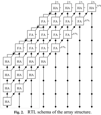
The second multiplication structure is based in the direct implementation of the traditional multiplication algorithm. Fig. 2 shows the RTL schema of the array structure composed by blocks called full adder, FA, and half adder, HA, that are able to sum three or two different bits respectively.
HA A*b0
A*b1
A*b3
A*b2
FA
a1 a0
a2
a3
HA HA HA
FA FA
FA
FA FA
FA FA
FA FA
FA FA
HA HA HA HA
HA HA HA
HA HA
HA
Fig. 2. RTL schema of the array structure.
In this case there two differences from respect the one that appear in [14]. First, the black circles that are the flip-flops needed for the pipeline; and second the three last
rows, surrounded by a doted line, included in order achieving a one FA delay operation (n-1 rows must be added for a n-bit width multiplier). Again, if pipeline is not needed all the flip-flops can not be synthesized. Latency depends linearly on the number of bits of the multiplier.
3.PHYSICAL DEVICES
The multiplication structures are going to be synthesized on two different devices. From Xilinx, XC4VSX55-12 has been selected, with 49.152 LUTs, of the Virtex4 family. From Altera, EP2S60F1020C5 is the chosen device, belonging to the StratixII family, has 48.532 ALUTS. With this choice we have two physical devices with almost the same logical capacity, that’s important because smaller devices can provoke bad power dissipation results due to bad signal routing. As synthesis software is going to be used ISE 8.1 for Xilinx and Quartus II 6.0 for Altera. Both device families, StratixII and Virtex4, contain a special circuitry to implement multiplication. So it’s possible to force the software synthesizer to use it by a specific VHDL code. The resulting multiplication structure uses an optimized hardware and transmission lines of the FPGA so they are going to be selected as a reference value. Power dissipation results are obtained by analyzing the netlist switching activity in a post place and route simulation of the multiplication structures. Since a FPGA is a physical device with fixed delays and power dissipation for each component we can expect close to real results. Simulation consists of 1000 different multiplications with just a 1% of multiplications by zero. The switching activity of the input operand bits from one operation to another is about 50% of them. Static power dissipation is constant for any design in the same device and I/O pin power dissipation depends on a higher power supply so both results aren’t going to be taking into account.
4.SYNTHESIS RESULTS FOR TEMPORAL PARALELISM
0 2500 5000 7500 10000 12500 15000
8 16 32 64
Bits of the operands
A
re
a
(
A
LU
Ts
)
Tree Array
Tree-Pipe Array-Pipe
Fig. 3. Logic resources occupation in Stratix II.
Logic resources occupation for the Virtex4 device, Fig. 4., repeats the same behavior than the StratixII one. Pipelined versions need more logic resources than combinational ones and, practically, in the same proportion. Tree multiplication structure need less logic resources in the StratixII family than in the Virtex4 due its more complex logic blocks, ALUTs, which are able to implement functions of up to six inputs. However, this functionality is less useful in a design like the array multiplication structure that is composed by three inputs functions and its results are similar to the Virtex4 family.
0 2500 5000 7500 10000 12500 15000
8 16 32 64
Bits of the operands
Area (L
UT
s)
Tree Array
Tree-Pipe Array-Pipe
Fig. 4. Logic resources occupation in Virtex4.
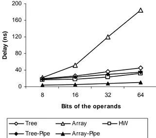
Continuing with the delay improvement in the StratixII family, Fig. 5 shows that both multiplication structures, thanks to the pipeline, can achieve working frequencies as
fast as the multiplication structure implemented with the special circuitry of the FPGA, HW.
0 40 80 120 160 200
8 16 32 64
Bits of the operands
D
e
la
y (
n
s)
Tree Array HW
Tree-Pipe Array-Pipe
Fig. 5. Multiplication structures delay in StratixII.
Array structure gets the biggest reduction since its critical path is reduced to just one FA. The behaviour of the tree structure is practically the same with or without the pipeline because its critical path depends mainly on the final conversion adder that is inside of one pipeline stage. Delay results for the Virtex4 family, Fig. 6, present practically the same graph that Fig. 5. Array multiplication structure is the slowest one, while the pipelined array structure becomes the fastest one approaching to the FPGA multiplication structure, HW. Again, tree structure doesn’t improve a lot.
0 40 80 120 160 200
8 16 32 64
Bits of the operands
D
el
ay (
n
s)
Tree Array HW
Tree-Pipe Array-Pipe
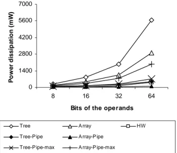
Fig. 7 shows how the power dissipation reduction when the pipeline is introduced in the StratixII family. The array multiplication structure with pipeline, at a working frequency that produces a result within the initial delay, called Array-Pipe in the graph, becomes the best in power dissipation. When the array multiplication structure is pushed to the maximum working frequency allowed by the pipeline, Array-Pipe-max in the graph, it maintains behaviour close to rest of the low power dissipation structures.
0 1400 2800 4200 5600 7000
8 16 32 64
Bits of the operands
P
ow
e
r d
is
s
ipa
ti
on
(m
W
)
Tree A rray HW
Tree-P ipe A rray-P ipe Serie6
Tree-P ipe-max A rray-P ipe-max
Fig. 7. Power dissipation on StratixII.
In the other hand, tree structure reduces too its power dissipation with the insertion of the pipeline, Tree-Pipe in the graph, with a position very close to the multiplication structure made by the FPGA blocks, HW. The graph called Tree-Pipe-max represents the pipelined tree structure working at the maximum frequency. In this case, there is just a small difference with the Tree-Pipe line due to the limitation of the working frequency of the pipeline as shown in Fig. 5
With the Virtex4 family, Fig. 8, we can see that, again, the structures with pipeline reduce mainly their power dissipation. Pipelined array is the one with less power dissipation when working at the initial frequency; but now there isn’t a very big difference when it is forced to the maximum frequency permitted by the pipeline.
The tree structure leaves the worst position and turns into the second best structure in power dissipation, better than multiplier structure of the FPGA. Increasing the working frequency to the maximum possible doesn’t produce a relevant change and the graph Tree-Pipe-max almost equals the Tree-Pipe graph.
0 1400 2800 4200 5600 7000
8 16 32 64
Bits of the operands
Power dissipa
ti
on (
m
W)
Tree Array HW
Tree-Pipe Array-Pipe Serie6
Tree-Pipe-max Array-Pipe-max
Fig. 8. Power dissipation on Virtex4.
The behaviour of the tree structure in both families is very similar there is an important reduction of the power dissipation thanks to the pipeline. However theorically there should be no power dissipation reduction. Taking into account that the dynamic power dissipation is usually calculated by the following equation:
2
fCV
P
Dynamic≈
α
(1)where α is the average number of transitions, f is the
working frequency, C is the capacitance of one transistor
and V is the power supply. The tree structures with and
without pipeline have the same C and V due to the physical
device, α doesn’t change because there is no new added logic and they have the same working frequency.
So the power dissipation reduction comes from the elimination of the glitch transmission through the circuit due to the registers used to implement the pipeline. The way as FPGAs connect two logic blocks produces several glitches that are the cause of the power dissipation.
Glitch importance is more clearly shown in the array structure. Pipelined structure produces a big reduction in power dissipation. But the distance between the two pipelined array structure graphs is not as big as can be expected from the difference between the two working frequencies.
5. CONCLUSION
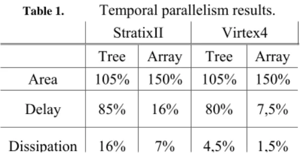
Table 1. Temporal parallelism results.
StratixII Virtex4
Tree Array Tree Array
Area 105% 150% 105% 150%
Delay 85% 16% 80% 7,5%
Dissipation 16% 7% 4,5% 1,5%
[8] C. Cao, M. O’Nils and B. Oelmann, “Synthesis tool for low-power finite-state machines with mixed synchronous/asynchronous state memory”, IEE Proc. Computers and Digital Techniques, vol. 153, no. 4, pp. 243-348, July 2006.
[9] J.S. Yuan and J. Di, “Teaching low-power electronic design in electrical and computer engineering”, IEEE Trans. Education, vol. 48, no. 1, pp. 169-182, Febreaury 2005.
[10] Y.-Y. Sung and R.C.Chang, "A novel CMOS double-edge triggered flip-flop for low-power applications", Proc. of Int. Symp. on Circuits and Systems, vol. 2, pp. 665-668, May 2004.
blocks of the modern FPGAs, mainly StratixII and Virtex4. Moreover, pipelining is very useful for glitch elimination
and, consequently, for power dissipation reduction. [11] E. Morifuji, T. Yoshida, M. Kanda, S. Matsuda, S. Yamada
and F. Matsouka, “Supply and threshold-voltage trends for scaled logic and SRAM MOSFETs”, IEEE Trans. Electronic Devices, vol. 53, no. 6, pp. 1427-1432, June 2006.
Tree structure maintains its timing behavior in both families while the array structure is able to reach very high working frequencies.
Finally, StratixII family seems to be more sensitive to the glitches propagation than the Virtex4 one, specially in the case of a structure in an array shape.
[12] E. Boemo, G. Gonzalez, S. Lopez-Buedo and J. Meneses, “Some Notes on Power Management on FPGA-Based Systems”, Lecture Notes in Computer Science, vol. 975, pp. 149-157, 1995.
6.REFERENCES [13] S.-W. Lee and J.-L. Gaudiot, “Throttling resource
management in high performance multithread”, IEEE Trans. Computers, vol. 55, no. 9, pp. 1142-1152, September 2006.
[1] M. Vratonjic, B.R. Zeydel and V.G. Oklobdzija, “Low and ultra low-power arithmetic units: design and comparison,” Proc. IEEE Int. Conf. on Computer Design: VLSI in Computers and Processors , pp. 249–252, Oct. 2005.
[14] K.-S. Chong, B.-H. Gwee, and J. Chang, “A low power 16-bit booth leapfrog array multiplier using dynamic adders,” in Proc. IEEE Int. Symp. on Circuits and Systems, vol. 2, pp. 23–26, May 2004.
[2] F. Carbognani, F. Buergin, N. Felber, H. Kaeslin and W. Fichtner, “42% power savings through glitch-reducing clocking strategy in a hearing aid application”, Proc. IEEE Int. Symp. on Circuits and Systems, pp. 2941-2944, October, 2006.
[15] Y. Liao and D. Roberts, “A high-performance and low-power 32-bit multiply-accumulate unit with Single-Instruction-Multiple-Data (SIMD) feature,” IEEE Journal of Solid-StateCircuits, vol. 37, no. 7, pp. 926–931, July 2002.
[3] M. Nakai, S. Akui, K. Seno, T. Meguro, T. Seki, T. Kondo, A. Hashiguchi, H. Kawahara, K. Kumano and M. Shimura, “Dynamic voltage and frequency management for a low-power embedded microprocessor”, IEEE Jour. Of Solid-State Circuits, vol. 40, no. 1, pp. 28-35, January 2005.
[16] M.A. Sacristan, V. Rodellar and A. Diaz, “Estructura multiplicadora reusable para DSP sobre FPGAs”, Proc. of Workshop on Reconfigurable Computing and Applications, September 2006.
[17] J.-P. Deschamps, G.J.A. Bioul and G.D. Sutter, “Synthesis of arithmetic circuits: FPGA, ASIC and embedded systems”, Wiley Interscience, 2006.
[4] A. Rettberg and F.J. Ramming, “A new design partitioning approach for low power high-level synthesis”, Proc. IEEE Int. Workshop on Electronic Design, Test and Applications,
pp. 6, January 2006. [18] M. Ercegovac and T. Lang, “Digital Arithmetic”. Morgan
Kaufman Publishers, 2004.
[5] R. Sanghamitra and B. Prith, “An algorithm for trading off quantization error with hardware resources for MATLAB-based FPGA design”, IEEE Trans. On Computers, vol. 54, no. 7, pp. 886-896, July 2005.
[19] B. Parhami, “Computer arithmetic”. Oxford University Press, 2000.
[20] W. Natter and B. Nowrouzian, “A novel multiplier recoding technique and its application to the development of a high-speed parallel online multiply-accumlate architecture,” in Proc. of IEEE Int. Symp. on Circuits and Systems, pp. 713– 716 May 2001.
[6] D.-S. Lee and I.-C. Park, “Low power log-MAP decoding based on reduced metric memory access”, IEEE Trans. On Circuits and Systems I: Regular Papers, vol. 53, no. 6, pp. 1244-1253, June 2006.
[21] B.D. Andreev, E.L. Titlebaum and E.G. Friedman, "Transformations of signed-binary number representations for efficient VLSI arithmetic", Proc. of IEEE Int. Workshop on System-on-Chip for Real-Time Applications, pp. 70-75, 2003.