Effect of the Synthesis Route on the Microstructure and the Dielectric
Behavior of CaCu
3Ti
40
1 2Ceramics
Miguel A. de la Rubia,
CaCu3TÍ4012 (CCTO) was prepared by a conventional synthe-sis (CS) and through reaction sintering, in which synthesynthe-sis and sintering of the material take place in one single step. The microstructure and the dielectric properties of CCTO have been studied by XRD, FE-SEM, EDS, AFM, and impedance spectroscopy to correlate structure, microstructure, and electri-cal properties. Samples prepared by reactive sintering show very similar dielectric behavior to those prepared by CS. Therefore, it is possible to prepare CCTO by means of a sin-gle-step processing method.
I. Introduction
R
ECENTLY, the compound CaCu3Ti401 2 (CCTO) hasattracted much interest due to its high dielectric
con-stant (up to 105), which is almost frequency-independent up
to 106 Hz, and shows good temperature stability in the range
between 100 K and 400 K.1 The main disadvantage of this
material is the high dielectric losses that limit its use. Although materials with very high dielectric constant are generally ferroelectric or relaxor, CCTO is centrosymmetric in the temperature range under study, and it does not present phase transition. The system presents distorted cubic perov-skite structure with an Im3 space group and a lattice
param-eter of 7.391 A- The TiOs octahedron is tilted and, as a
consequence, the coordination of Ca and Cu cations is altered, producing a square planar arrangement of the
oxy-gen around the Cu2 + cations and a 12-coordinate
icosahe-dral environment for Ca.2
The origin of the high dielectric constant of CCTO is still a source of controversy. Intrinsic effects such as stoichiome-tric changes, oxygen vacancies, Cu segregation and different oxidation states of Ti and Cu could result in high dielectric constant via extrinsic effects related to the microstructure, as stated by the Internal Barrier Layer Capacitance (IBLC) model. According to this model, the material can be consid-ered as an ensemble of w-type semiconducting CCTO grains and insulating barriers, corresponding to a very thin Cu-rich
secondary phase observed at the grain boundary.3'4 This
characteristic microstructure with semiconducting grains and insulating barriers (including domain boundaries and grain boundaries) results in electrostatic barriers at the grain boundaries, which are responsible for the nonlinear current-voltage behavior that this material presents. Oxygen vacan-cies may be proposed as a possible cause for the electron
for-Pilar Leret Jose de Frutos, and José F. Fernández
mation.5 At room temperature, dc resistivity of undoped
CCTO is principally determined by the grain boundary resis-tivity and therefore this resisresis-tivity depends on processing. There are very few reports related to the impurity effect on CCTO. In CCTO ceramics, a clear increase of the dielectric constant has been observed with sintering time due to the incorporation of the Cu-rich grain boundary secondary phase
into the CCTO grains.6
The electrical properties of both doped and undoped CCTO depend as much on the raw materials as on
process-ing.7 Reaction sintering method has never before been used
to prepare CCTO.
The aim of this work was to study CaCu3Ti401 2 ceramics
prepared by reaction sintering without an intermediate calci-nation step, and to compare these materials with the ones prepared by a conventional synthesis method.
II. Experimental Procedure
Ceramic samples of CaCu3Ti401 2 were prepared by two
dif-ferent synthesis routes: the conventional solid-state reaction (CS) and by means of reaction sintering (RS). In all cases,
Ti02 powder (anatase, 99.9%, Merck, d50 = 0.5 \im;
Darm-stadt, Germany), CuO (99.9%, Aldrich, d50 = 3.3 pm;
Madrid, Spain), and C a C 03 (Aldrich, <5?50 = 0.9 \im) were
mixed in attrition mill for 3 h with zirconia balls using de-ion-ized water and 0.3 wt% of Dolapix C64 as dispersant. The milled powders were dried and sieved through 100 \im mesh.
Conventional solid state reaction consisted of the calcina-tion at 900°C-12 h of the milled mixture of raw materials in adequate amounts (synthesis of CCTO). Then the CS synthe-sized powder was attrition milled for 3 h (after milling <5?5o = 0.8 \im). Dry powders were pressed into disks of 8 mm in diameter and 1.3 mm in thickness at 200 MPa by using 0.6 wt% of polyvinyl alcohol PVA and 0.3 wt% of polyeth-ylene glycol PEG as organic binders to favor the pressing step. The disks were sintered at 1100°C-32 h. In the reaction sintering method, RS, the synthesis and sintering of CCTO pellets were carried out in the same step at 1100°C for 32 h. All thermal treatments were carried out with a heating and cooling rate of 3°C/min. The density of the samples for both
synthesis routes after sintering was > 4 . 8 g / c m3 (>95% of
the theoretical density). Samples prepared by reaction sinter-ing shrunk - 6 % more in diameter than conventional synthe-sis ones. X-ray diffraction analysynthe-sis was performed on a diffractometer X'Pert PRO of Panalytical using CuiSxl radi-ation. RS samples were polished and thermally etched at 1000°C for 5 min. The microstructure was observed by using a Hitachi SEM TM-1000 (Krefeld, Germany). To perform the electrical characterization, polished parallel disks were electroded with Pt by sputtering with a DSC-050 of BAL-TEC (Wetzlar, Germany). Dielectric characterization was
measured at RT in the range 10~2 H z - l M H z in a Solartron
III. Results and Discussion
Figure 1 shows the XRD pattern of the CS powder calcined at 900°C-12 h. For a better analysis of the spectra, the loga-rithmic scale has been used, resolving the noise of the spectra and provoking the enlargement of minor peaks that in linear scale are not easily detected. XRD analysis of the calcined powder shows the presence of the perovskite CCTO phase without traces of secondary phases or unreacted raw materi-als. XRD analysis of the sintered CCTO samples (Fig. 2) shows that, regardless of the processing method CS or RS, only the perovskite CCTO phase is identified. The sintering
of CS samples occurs in solid state because there is no T i 02
nor CuO unreacted raw materials available, to develop the
eutectic liquid around 1000°C8 that assists sintering.
How-ever, in RS, the elimination of the calcination step allows a
20 30 40 50 60 70
29
(°)
Fig. 1. XRD of raw material calcined at 900°C-12 h.
10 i
o
• o CD
1 io_N E o
c 10"
(a)
ílÉliiLlJllHiii^J
p
u
V
UyyU
20 30 40 50 60 70
29 (°)
20 30 40 50 60 70
29 (°)
Fig. 2. XRD of sintered CCTO samples, (a) CS and (b) RS.
possible reaction between CuO and T i 02 at high temperature
(~1000°C) to form the eutectic liquid that can assist the first steps of sintering.
The SEM characterization of polished and thermally etched samples shows similar micro structures for both syn-thesis routes (Fig. 3). Sintered samples from both routes show a bimodal grain size micro structure that is slightly more marked in the CS sample. In the CS sample, there are regions of small grains with thick Cu-rich intergranular phase; however, in RS samples, some grain boundaries have a very thin Cu-rich secondary phase (Fig. 4). The Cu-rich secondary phase recrystallizes in the grain boundary during the thermal etching treatment, and it is identified by XRD analysis (Fig. 5). The large amount of secondary phase observed in the micro structure of Fig. 3 is associated with a
surface effect, in agreement with other authors.9 Prakash and
Varma9 indicated that there is a preferential segregation of
the Cu-rich phase on the surface due to inhomogeneous dis-tribution of oxygen on the surface and in the interior of the sample. This Cu-rich phase disappears thinning out a few layers from the top and the bottom surfaces. For a better observation of the micro structure, the samples were thermi-cally etched, favoring the segregation and recrystalhzation of the Cu-rich phase over the surface of the samples. Moreover, other microstructural features of CCTO as domain bound-aries are very sensitive to the etching thermal treatment
according to literature.10'11 In the same way,
Fig. 4. SEM micrographs of the Cu-rich intergranular phase in CCTO samples polished and thermally etched, (a) CS and (b) RS.
Fritsch et al. show microstructures with a large and thick amount of Cu-rich secondary phase and a very high dielec-tric response.
Table I summarizes the RT impedance characteristics of CCTO samples. Grain and grain boundary resistance are considered as the intercept of the bulk (g) and grain bound-ary (gb) semicircles, respectively, with the real part of the
impedance. Using the relationship 2nfmaxRgCg = 1 and
^Ti/max^gb^gb = 1 at the impedance semicircle maximum, the Cg and Cgb values were obtained. Z'-Z" plots for CS and RS samples (Fig. 6a) apparently show only one semicircle corresponding to the insulating grain boundary region, but if we compare the semicircle shape in the different frequency regions, we can consider several arc superpositions. More than one arc can fit the data related to interfacial relaxation phenomena (Maxwell-Wagner-Sillars) associated with differ-ent grain boundaries. The semicircles do not intercept the Z'-axis in cero at high frequency, and these resistances corre-spond to the semiconducting grain regions, (Rg ~ 350 and 270) for CS an RS samples, respectively (Fig 6b). These
val-ues are in agreement with the one reported by Adams et al.13
The semicircles assigned to the grain boundary regions showed higher impedance 0.56 and 1.2 MO, for CS and RS samples, respectively. Capacitance values associated with
grain boundaries for CS and RS are 9.1 x 1(T9 and
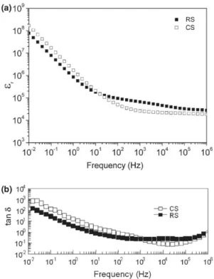
2.7 x 10~8 F, respectively. Figures 7a and b show the
rela-tive dielectric constant (sr) and the dielectric losses (tan 5) in
Fig. 5. XRD of sintered, polished, and thermally etched CCTO ceramics samples, (a) CS and (b) RS.
Table I. Resistance (ST) and Capacitance (F) Values for Grains and Grain Boundaries of the Different Samples
Prepared by Both Synthesis Routes
Sample
CS RS
Grain
35 27
R(Q)
Grain boundary
5.6 x 10⁵
1.2 x 10⁶
Grain
-C ( F )
Grain boundary
9.1 x 1(T9
2.7 x 1(T8
a wide frequency range for both processing methods. The dielectric constant and losses show slight differences in the
dielectric behavior in the frequency range between 105 and
101 Hz such as the dielectric constant for RS sample
pos-sesses higher frequency dependence. The dielectric losses for RS samples show lower frequency dependence in this frequency range. Both characteristics decrease with the
frequency increase. At high frequency values (102-106 Hz),
the dielectric constant for the RS sample is slightly higher than for the CS one; both are almost frequency-independent, exhibiting the same tendency as the real component of the permittivity, s', which is associated with capacitive
phenom-ena. In this frequency range, relative permittivity (sr) values
for RS and CS samples are approximately 6.6 x 10⁴ and
2.6 x 10⁴, respectively (Fig. 7a). These values are
compara-ble to the ones previously reported in the literature.1 '14'15
Dielectric losses are low (~10_1) and slightly higher for the
RS sample than for the CS one, although the RS sample shows lower dependence of the frequency (Fig. 7b). At lower
frequencies (<102 Hz), the dielectric constant for CS sample
-1x10⁶
N
-5x10
sh
5,0x10⁶ 1,0x10⁶ 1,5x10⁶
Z'
-300
-200 h
N
-iooh
100
f
f/
;
|
(b)
-D-CS
- • - R S
100
200
Z"
300
400
Fig. 6. Z'-Z" plots for sintered CCTO samples for different
processing methods, (a) All frequencies range and (b) Zoom of the high frequency.
conductive phenomena. From 102 to 106 Hz, the grain's
inte-rior dominates the electrical response with high 8 values
between 6.6 x 10⁴ and 2.6 x 10⁴, and at lower frequencies
(10~2-10° Hz), the giant dielectric response (108-106) of
CCTO ceramics is associated with conduction processes that occur in the grain boundary region, although it is
accompa-nied by high dielectric losses (103—101).16 According to
com-plex impedance analysis, the grain's interior dominates the
electrical response at high frequencies (~106 Hz), but the
dielectric behavior in all the frequency range is related to interfacial relaxation phenomena. This relaxation known as Maxwell-Wagner-Sillars is due to the displacement of the trapped charge in the interfaces that is development in heter-ogeneous dielectric materials such as CCTO, associated with grain boundaries and in agreement with the IBLC model. When phases of a ceramic have different conductivities such as in CCTO, imposition of an electric field causes the move-ment of charge from the more conductive phase toward the
less conductive one.17 At lower frequencies (10~2-1 Hz), an
increase in the dielectric constant that takes place may be assigned to the space charge interfacial polarization effects. The high dielectric constant at low frequencies is accompa-nied by very high dielectric losses. The dielectric loss is con-siderably higher especially at low frequencies, which is mainly attributed to inhomogeneous conduction vis-á-vis
interfacial polarization.18 The copper-rich liquid phase during
the sintering process probably favors the grain-shell wetting, leading to multilayered materials where the charge carriers' concentration at the different interfaces rises as the copper
10~2 10~1 10° 101 102 103 104 105 106
Frequency (Hz)
ia2 ia1 icP io1 id2 icP icf 105 id3
Frequency (Hz)
Fig. 7. (a) Frequency dependence of dielectric constant (s) and (b) dielectric loss of CCTO samples for both synthesis routes (RS, reaction sintering; CS, conventional synthesis).
amount increases. Charge accumulation on both sides of the boundary layers provokes an increase in the dielectric con-stant of the samples accompanied by an increase in the dielectric losses. Other authors suggest that the dielectric losses increase is associated with a pure conduction
mecha-nism described by the G/OOS0 ratio.12 In the same manner, at
lower frequencies, conduction losses due to space charge relaxation, which usually result in the increase in the dielec-tric constant, become relevant. Nonhomogeneous materials like porous materials, polycrystalline or with a lot of defects can show at the lowest frequencies an increase in the real part of the dielectric constant. This effect also takes place in
heterogeneous materials composed of two or more phases.19
Based on these results and the micro structural character-ization, it can be deduced that the dielectric response is clo-sely related to the micro structure and the Cu-rich
intergranular phase. According to the IBLC model,12'13'15'20
the effective dielectric constant (eeff) is directly proportional
to the average grain size (tg) and inversely proportional to
the grain boundary thickness (igb) as seff = er (tg/tgh) where sr
is the relative permittivity. Samples obtained by both pro-cessing methods (CS and RS) show similar micro structures (bimodal grain size with similar amount of Cu-rich secondary phase in grain boundaries), although they show slight differ-ences in the dielectric behavior in the frequency range
between 105 and 101 Hz such as the dielectric constant for
RS samples possesses higher frequency dependence. Both samples are in agreement with the IBLC model, where the resistance of the grain is lower than the grain boundary one (Table I). According to this model and in agreement with the obtained results, the sample that shows higher dielectric (RS) is the one in which the differences in conduction between grain and grain boundaries are higher (Table I). Point out that the samples obtained by both processing methods show very high dielectric constants accompanied by low dielectric losses in a wide frequency range (102 Hz-1 MHz).
IV. Conclusions
microstructures (bimodal grain size with similar amount of Cu-rich secondary phase in grain boundaries), although they show slight differences in the dielectric behavior in the
fre-quency range between 105 and 101 Hz such as the dielectric
constant for RS samples possesses higher frequency depen-dence. In this frequency range, the sample that shows that higher dielectric constant (RS) is the one in which the differ-ences in conduction between grain and grain boundaries are higher in agreement with the IBLC model. In both samples, the very high dielectric response is accompanied by low dielectric losses, exhibiting the same trend as the real compo-nent of the permittivity, &', which is associated with
capaci-tive phenomena. At lower frequencies (<101 Hz), the giant
dielectric constant for CS sample is slightly higher than the RS one, although it is accompanied by higher dielectric losses. This behavior follows the same trend as the one exhibited by the imaginary component of the permittivity s" related to conductive phenomena. It has been possible to
obtain CaCu3Ti401 2 ceramics with very high dielectric
con-stant by means of reaction sintering and therefore without an intermediate calcination step. This is the first time that CCTO ceramics are prepared in a single step, performing synthesis and sintering in only one thermal treatment.
Acknowledgments
This work has been financially supported by the Spanish Ministry of Science and Innovation under the program MAT2010-21088-C03-01 and 02.
References
'M. A. Subramanian, D. Li, N. Duan, B. A. Reisner, and A. W. Sleight, "High Dielectric Constant in ACu3Ti4012 and ACu3Ti3Fe01 2 Phases," /.
Solid State Chem., 151 [2] 323 (2000).
2B. Bochu, M. N. Deschizeaux, J. C. Joubert, A. Collomb, J. Chenavas, and M. Marezio, "Synthése et Caractérisation d'une Serie de Titanates Perovskites Isotypes de CaCu3Mn401 2," / . Solid State Chem., 29, 291-8 (1979).
3J. F. Fernández, P. Leret, J. Frutos, M. A. de la Rubia, M. S. Martín-Gon-zález, J. L. Costa Kramer, J. L. G. Fierro, A. Quesada, and M. A. Garcia, "Proof for co-Existence of two Magnetic Contributions in Pure and Doped CaCu3Ti401 2 Giant Dielectric Constant Ceramics," J. Am. Ceram. Soc, 92
[10] 2311-8 (2009).
4P. Leret, J. Fernandez, J. de Frutos, and D. Fernandez- Hevia, "Nonlinear
I-V Behaviour of Doped CaCu3Ti401 2 Ceramics," J. Eur. Ceram. Soc, 27,
3091-905 (2007).
5D. C. Sinclair, T. B. Adams, F. D. Morrison, and A. R. West, "One Step
Internal Barrier Layer Capacitor," Appl. Phys. Lett., 80 [12] 2153-5 (2002).
6J. J. Romero, P. Leret, F. Rubio-Marcos, A. Quesada, and J. Fernandez,
"Evolution of the Intergranular Phase During Sintering of CaCu3Ti401 2
Ceramics," /. Eur. Ceram. Soc, 30 [3] 737-42 (2010).
7P. Leret, M. A. de la Rubia, F. Rubio-Marcos, J. J. Romero, and J. F. Fernández, "Effect of Processing on the Sintering of High Dielectric Constant CaCu3Ti401 2 Ceramics," Int. J. Appl. Ceram. Technol, 8, 1201-7 (2011).
8M. A. de la Rubia, P. Leret, J. J. Reinosa, J. J. Romero, J. de Frutos, and J. F. Fernandez, "Experimental Determination of the Eutectic Temperature in Air of the CuO-Ti02 Pseudobinary System," J. Eur. Ceram. Soc, 32 [1] 71-6 (2012).
9B. S. Prakash and K. B. R. Varma, "Influence of Sintering Conditions and Doping on the Dielectric Relaxation Originating From the Surface Layer Effects in CaCu3Ti401 2 Ceramics," /. Phys. Chem. Solids, 68, 490-502 (2007).
10T. T. Fang and H. K. Shiau, "Mechanism for Developing the Boundary Barrier Layers of CaCu3Ti401 2," / . Am. Ceram. Soc, 87 [11] 2072-9 (2004).
nT . T. Fang and C. P. Liu, "Evidence of the Internal Domains for Inducing the Anomalously High Dielectric Constant of CaCu3Ti401 2," Chem. Mater.,
17, 5167-71 (2005).
12S. Guillemet-Fritsch, T. Lebey, M. Boulos, and B. Durant, "Dielectric Properties of CaCu3Ti401 2 Based Multiphased Ceramics," J. Eur. Ceram. Soc, 26, 1245-57 (2006).
13T. B. Adams, D. C. Sinclair, and A. R. West, "Influence of Processing
Conditions on the Electrical Properties of CaCu3Ti401 2 Ceramics," J. Am. Ceram. Soc, 89 [10] 3129-35 (2006).
14L. Liu, H. Fan, X. Chen, and P. Fang, "Electrical Properties and
Micro-structural Characteristics of Nonstoichiometric CaCu3 xTi401 2 Ceramics,"
/. Alloys Compd, 469, 529-34 (2009).
15M. Pan and B. A. Bender, "A Bimodal Grain Size Model for Predicting the Dielectric Constant of Calcium Copper Titanate Ceramics," J. Am. Ceram.
Soc, 88, 2611-4 (2005).
16P. Leret, M. A. de la Rubia, J. J. Romero, J. de Frutos, and J. F. Fernan-dez, "Phenomenological Model of Grain Boundary Behaviour Under a Bias Field in Nb-Doped CaCu3Ti401 2 Ceramics," / . Alloy. Compd., 509 [41] 9719-23 (2011).
R. C. Buchanan, Ceramic Materials for Electronics Processing, Properties
and Applications, p. 114, Crc. Press, New York, 1991.
18P. Thomas, S. Satapathy, K. Dwarakanath, and K. B. R. Varma,
"Dielec-tric Properties of Poly(Vinylidene Fluoride)/CaCu3Ti4Oi2 Nanocrystal
Com-posite Thick Films," Express Polym. Lett., 4 [10] 632-43 (2010).
19J. M. Albella and J. M. Martin, Physics of Dielectrics. Chap. 5-6, Ed.
Marcombo, Barcelona, 1984.
20A. J. Moulson and J. M. Herbert Electroceramics: "Materials, Properties