High precision pressure sensors based on SAW devices in the GHz range
J.G. Rodriguez-Madrid , G.F. Iriarte , O.A. Williams , F. Calle
A B S T R A C T
In this paper, an AIN/free-standing nanocrystalline diamond (NCD) system is proposed in order to process high frequency surface acoustic wave (SAW) resonators for sensing applications. The main problem of synthetic diamond is its high surface roughness that worsens the sputtered AIN quality and hence the device response. In order to study the feasibility of this structure, AIN films from 150 nm up to 1200 nm thick have been deposited on free-standing NCD. We have then analysed the influence of the AIN layer thickness on its crystal quality and device response. Optimized thin films of 300 nm have been used to fabricate of one-port SAW resonators operating in the 10-14 GHz frequency range. A SAW based sensor pressure with a sensibility of 0.33 MHz/bar has been fabricated.
1. Introduction
For the last few decades, surface acoustic wave devices have been used not only for wireless communication systems [1], but also for gas [2-4], temperature and pressure sensors [5-7] due to their intrinsic energy confinement in a narrow region underneath the surface. Furthermore, the interest in tyre pressure monitoring systems (TPMS) for the automotive industry has increased in recent years. First generation of TPMS was based on MEMS pressure sen-sors and battery-powered active transmitters positioned in every wheel [8]. The use of SAW sensors offers the most promising solu-tion for batteryless second generasolu-tion TPMS [9,10]. In a longer term, implantable blood pressure sensors are envisioned.
Different factors are under consideration in the selection of a suitable substrate for SAW sensors, including the electromechani-cal coupling coefficient (k2), the surface acoustic wave velocity, and the temperature coefficient of delay (TCD). Moreover, the sensitiv-ity increases for higher frequencies [11]. The central frequency of a SAW resonator, given b y / = v/k, depends on many physical param-eters. Each material has a phase velocity, v, and k is the wavelength corresponding to the period of the interdigital transducers (IDTs). These are not the only parameters that can be changed in order to modify the central frequency. In a slow on fast structure such as the one used for this work, the substrate material and the piezoelectric
film thickness play an important role to determine the resonance of the device under test, as discussed previously [12].
Eqs. (1) and (la) show the linear approximation of the SAW res-onator frequency dependence on pressure when the temperature is kept constant.
/ ( p ) = / o + S * ( p - p0) (1)
S*=foS (la)
where po is a reference value and S is the first order pressure coefficient [13]. The higher the central frequency, the higher the shift in the frequency for the same pressure change.
M | i m ^
Glue
IDT
Silicon chemical etching and AIN deposit
I
PhotoresistIDT metallization
AUO,
Exposure of the nano IDTs [bye-beam lithography)
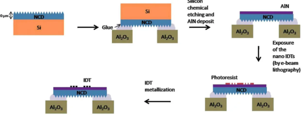
Fig. 1. Schematic process followed to obtain the free-standing diamond used to deposit AIN and process SAW device sensors.
CVD nano-crystalline diamond on silicon has been used in this work to deposit AIN films by reactive sputtering. The principal dis-advantage of this synthetic diamond is its high surface roughness. Several methods have been proposed to overcome this problem [19]. Mechanical polishing of the diamond surface has been used for microcrystalline diamond (MCD) in order to solve it [20,21 ]. How-ever, this procedure is expensive, time-consuming and not yet opti-mized for NCD. Some works have proposed alternative methods in order to overcome these disadvantages. These consist of using the smooth unpolished nucleation side of freestanding diamond layers [22-24]. This solution requires the whole Si substrate to be sacrifi-cially etched. At least 100 |jim thick films are required for structural stability, and thus this method is expensive, as the growth of a free-standing diamond film is a long duration process (approx. 1 |jim/h). However, in this work, an alumina substrate was used to get a more robust structure so the thickness requirement was alleviated; in this case, 20 |jim thick diamond films were employed. Moreover, the achieved frequency for the devices processed on 100 |jim films is below 1 GHz, far less than reported here.
Apart from the surface roughness, different technological requirements must be satisfied in order to obtain high frequency devices. The quality of the c-axis AIN film and hence its piezo-electricity is thickness dependent [25]. Furthermore, low surface roughness and small grain size are closely connected with low propagation losses [26].
In this work, we use a 20 |jim thick NCD, free standing mem-brane, whose silicon substrate was removed by chemical etching, to fabricate high frequency SAW resonators for mechanical sensors. This structure not only allows deposition of highly c-axis oriented AIN due to the low surface roughness of the nucleation side, but also the membrane is free to move so it provides pressure sensitivity. Furthermore, in some sensor systems, the property to be analysed can be more precisely controlled if a cavity can be fabricated in the structure [27].
Table 1
Processing conditions used during the reactive sputtering of AIN on diamond substrates.
Parameter Value
Power [W] Base pressure [mbar] Gas composition Ar/N2 [seem] Process pressure [mTorr] Substrate temperature [°C] Target substrate distance [mm] Target diameter [mm] Target thickness [mm] Deposition rate [nm/min]
700 <5x 3/9 3 25 45 101.6 6.35 80
10-On the other hand, the choice of the piezoelectric film thickness implies a compromise between the frequency and the intensity of the targeted resonances, as discussed previously [12]. Here, the influence of the AIN thickness on the SAW response of these free-standing structures is studied. The optimum AIN thickness was found to be 300 nm and allows manufacturing high performance and high frequency SAW resonators working above 10 GHz, with similar performance as those achieved before on polished MCD [28]. A sensitivity of 0.33 MHz/bar was observed under pressure conditions.
2. Experimental
NCD substrates were used to fabricate a free-standing structure by using the nucleation side of the NCD to deposit the AIN thin films. The procedure is summarized in Fig. 1. A home built balanced magnetron sputter deposition system was used to deposit the piezoelectric film. NCD substrates were grown on silicon accord-ing processes published elsewhere [29]. The rough side of the NCD was glued with an epoxy adhesive to an alumina substrate with a hole in the middle. The silicon substrate was removed by HF:HN03 2:1 chemical etching at room temperature. NCD films from 2 |jim-to 20 |jim-thick were used |jim-to obtain free-standing diamond. The 20 |jim-thick NCD is the only film that did not break during the processing to obtain the free-standing diamond.
The substrates were cleaned using a standard procedure before each deposit: rinsing in pirrolidone for 5 min at 80°C, acetone for 5 min at 60 °C and methanol in an ultrasonic bath. The sputtering conditions were optimized in order to obtain highly c-axis oriented AIN at low temperature, determined by X-ray diffraction (XRD) as described elsewhere in [ 12]. The crystallographic structure of these
AIN/Diamond
Glass holder
I
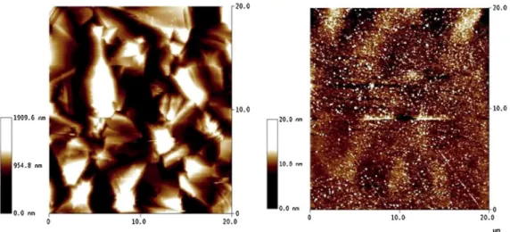
Fig. 3. AFM micrographs of rough (a) and nucleation side surface (b) of NCD.
films was examined using a Phillips X-Pert Pro MRD diffractometer. Although the diamond grains were randomly oriented, only the peak corresponding to the (111) direction appeared in the spectra. A1N films of approximately 150 nm-, 300 nm-, 600 nm- and 1.2 |jim-thick were deposited on free-standing NCD substrates under the conditions shown in Table 1.
Aluminium IDTs were fabricated by e-beam lithography with Crestec CABL-9500C equipment. The periodicity of the finger pairs was nominally 800 nm, i.e. finger width and pitch of 200 nm. The number of periods was 100 for both, the IDT and the reflector. Once the process was optimized, the reflection function of the devices was measured with an Agilent N5230A vector network ana-lyzer using coplanar-waveguide probe tips and standard calibration techniques.
Nitrogen gas in a pressure range of 2-5 bars was used to measure the pressure sensitivity of the SAW sensor. A schematic illustration of our SAW pressure measurement configuration is shown in Fig. 2. The SAW sensor was located on the edge of a 5 mm2 diaphragm and a pressure controlled nitrogen gas flow was located approxi-mately 5 mm above the membrane. The pressure underneath the AIN/diamond structure was kept constant at atmospheric pressure. The pressure applied to the membrane results from the difference (Ap) between the pressure applied on top (PI) and the atmospheric pressure underneath the AIN/diamond membrane (P2).
3. Results and discussion
were deposited on free-standing NCD. Fig. 4 shows the XRD spec-tra in the Q\2Q scan mode of these A1N films. The A1N films are highly oriented in the (0 0 0 2) direction, i.e. perpendicular to the substrate surface. The intensity of this peak is reduced when reduc-ing the film thickness. This behaviour is also observed on the A1N sputtered on polished MCD [12]. As it is shown in [31], a similar behaviour occurs when the A1N is sputtered on free-standing NCD; the A1N layer grows along the (0 0 0 2) direction but showing a two-domain structure with two in-plane orientations. This explains the co-existence of the main peak at 36.16° and the one at 35.3° cor-responding to the (0 0 0 2) direction. For the substrate grains, only the peak corresponding to the diamond (111) direction appears on the spectra.
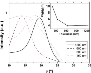
In order to evaluate the crystal quality and hence the piezo-electricity of these A1N films grown on free-standing NCD, the (0 0 0 2)-rocking curve was analysed. Fig. 5 shows the FWHM of the rocking curve peaks obtained in several films, which is reduced for thicker A1N layers, down to 4° for the 1200 m-and 600 nm-thick layers.
3.2. AIN thickness influence on the SAW response
Fig. 6 shows the reflection coefficient of a SAW resonator of k = 800 nm fabricated on 1200 , 600 , 300 and 150 nm-thick AIN sputtered on the free-standing NCD (solid line) and on
3.1. AIN sputtering on free-standing diamond
Highly oriented (0 0 0 2) AIN is a requisite for piezoelectric films and thus, to transfer the electrical signal efficiently into a SAW prop-agating on the diamond. In particular, the narrower the full width at half maximum (FWHM) of the (0 0 0 2)-rocking curve the bet-ter; according to our and previous results on sputtered AIN [30], it should typically be smaller than 4° in order to yield a strong piezoelectric response. Moreover, as described elsewhere [12,25], the surface roughness hinders the synthesis of c-axis oriented AIN. In order to overcome this difficulty, the nucleation side of a free-standing NCD layer is proposed here. Fig. 3 shows the height AFM micrographs of the top surface (a) and the bottom nucleation side (b) of NCD films. The average surface roughness improves from 262 nm root mean square (rms) for the rough NCD face, to 2nm rms for the free-standing NCD presented here.
XRD analyses, in the Q\2Q and rocking curve scan mode, were carried out to determine the crystallinity and orientation of the films. AIN films with thickness ranging from 150nm to 1.2|jim
co 3,0
2,5
2,0-AIN (002) -1200 nm 600 nm
- 300 nm -150 nm
Diamond (111)
ifmmmmtt*
40
9/26 (°)
Fig. 4. 6¡26 XRD spectra for AIN layers of different thicknesses.
3
3,
5
v>
c
I . I
C 10 E
1
8
'*"\
> - S\ 6
/ \
' / \
/ '\
/ A
4
/•••''
y \
\
i
300 600 900 1200 Thickness (nm)
v ^ -
\
i i i i '
1200 nm
600 nm
300 nm
150 nm
i '
10 15 20 25 30 35
en
Fig. 5. Rocking curves on the 0 0 0 2 direction of different thickness of AIN sputtered
on free-standing NCD. The inset shows the FWHM of the peak.
polished MCD (dash line). The film-thickness-to-wavelength ratio (H¡k) are kH=2TiHjk = 9A2, 4.71, 2.36 and 1.18, respectively. As it was presented elsewhere [28], the electromechanical coupling coefficient (K2) and the propagation velocity of the acoustic waves depend on the H/k. By decreasing the piezoelectric film thickness (small H/k), its crystal quality and orientation decrease, thus the piezoelectricity worsens. However, the SAW extends far into the diamond substrate, and the phase velocity (v) approaches the large
«
n
-10
-20
-30
-40
n
-10--20
-30
-40
é
-10
-20--30
-40;
0
-1U
-20 -30
-40
S1 ( S2
a)
1200 nm
?
~~vr~
b) s i
600 nm
f
c)
300 nm
f
d)
150 nm
i i
S3 S4
Freestanding NCD
MCD J
" i f - ,
* *-S2 S3 S4
»>
! si
I I I
¿j
—v S1
^
f
Í
10 12 14
Frequency (GHz)
Fig. 6. Reflection coefficient (Sn) spectra for identical (X = 800 nm) one-port SAW resonators on (a) 1200 nm-, (b) 600 nm-, (c) 300 nm-, and (d) 150 nm-thick AIN films on free-standing nanocrystalline diamond and polished microcrystalline diamond. R and S¡ denote the Rayleigh and Sezawa modes, respectively.
velocity value of the bare substrate. When the AIN thickness is higher than one period (800 nm), the crystal quality improves but the SAW concentrates in the piezoelectric film region, thus K2 is large but v is much smaller. This effect can be observed on Fig. 6. For the device fabricated on free-standing NCD, the v obtained for the first Sezawa mode, Si, increases from 7816 m/s for the 1200 nm-thick AIN, to 8425 m/s for the 600 nm-nm-thick AIN, 9995 m/s for the 300 nm-thick AIN and 10,751 m/s for the 150 nm-thick AIN. In addi-tion, the out-of-band rejection and quality factor Q. also improve when the AIN thickness is reduced until 300 nm. Furthermore, for the 150 nm-thick AIN device, the response is degraded due to the fact that the crystal quality also worsens for this narrow film thick-ness range, a behaviour common to all the observed modes. The difference observed in all frequency modes in the devices processed on polished MCD, when compared to those in free-standing NCD, is due to differences in the AIN thickness.
The choice of the piezoelectric film thickness implies a com-promise between the frequency and the intensity of the targeted resonances. For the structure presented in this work, the optimal AIN film thickness is 300 nm. The principal resonance for the SAW one port resonator fabricated on this film is 12.5 GHz, correspond-ing to the first Sezawa mode, and it shows a Q. factor of 643 and an out of band rejection of 11 dB. The Qand out of band rejection are better for the device processed on A1N/MCD due to the bet-ter quality of the AIN film [28]. Nevertheless, the results obtained for the devices processed on AIN/free-standing NCD are the high-est obtained so far on nanocrystalline diamond [32]. Moreover, the achieved frequency is the highest obtained among other free-standing NCD structures [22-24]. In addition, these results are in agreement with the ones obtained before [28], and confirm that the AIN/free-standing NCD structure is an alternative to the more expensive polished MCD for the processing of high performance and high frequency SAW devices.
3.3. SAW pressure sensor
-4
ST
• D
£
« -5
-6
"V
-as%
% *
1 bar 1,5 bar 2 bar 2.5 baJ 3 bar 3,5 baJ 4 bail
l£$ ú
\
i
• \ /
• . i .
i M
</
//
/
1
'
10770 10780 10790 10800
Frequency (MHz)
-DC -D
(0
m
•n
to"
-b,4
-5,7
-6,0
v<". \ \ \ '
v*.\\ '. 0-,
\ • S \ - •. V
v
-
\ \
'• V-,
\ \ v . ', \ \
<-.\\
•* • , v\ V
\ \ \v
- v .
-.
v-' ^ • N X
N • \ > • • • > .
>•' "'.its 'OÜL*
10784 10786 10788
Frequency (MHz)
-5,0
•5,2
-5,4
•5,6
•5,8
-6,0
S - \ * ••. i.
15 C % "•• v
vJ i - '-, »
*X\\
^ . v \ \
1 , 1 . r*" ' .
10780 10790 10800
Frequency (MHz)
10784 10786 10788
Frequency (MHz)
Fig. 7. Frequency response of AIN/diamond SAW resonators under: (a) upwards pressure variation (left), zoom in (right): (b) downwards pressure variation (left), zoom in (right).
Pressure up:
-Pressure down:
•
-•/
j/¡Jfi
%f
A
•
^^^~
•/^
I
^
•
'r*y^
I 10,7892
N
X
o
—" 10,7888
O ¡=
<I> 10,7884
10,7880
1 2 3 4
APressure (bar)
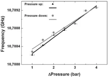
Fig. 8. Experimental frequency shift when pressure is applied in positive (up) and negative (down) direction (symbols) and linear regression for both (solid line).
substrate (together with an optimal membrane size and SAW device location on top of it), could be used in order to overcome the non linear behaviour and eliminate those temperature effects. The sensitivity obtained by linear fitting is 0.33 ± 0.02 MHz/bar as shown in Fig. 8. The high sensitivity obtained here can utterly be tuned up by optimizing the device location within the diaphragm [35,36].
4. Conclusions
A free-standing NCD structure is proposed as an alternative to polished MCD in order to sputter AIN and fabricate SAW devices for high frequency sensor applications. The influence of the
piezoelectric film thickness on the SAW response has been ana-lysed, and the optimum AIN layer thickness in our experiments results in 300 nm. The main resonance of a device obtained using this film with an IDT period of 800 nm is at 12.5 GHz, correspond-ing to the first Sezawa mode, and it shows a Q_ factor of 643 and an out-of-band rejection of 11 dB. As the membrane of the structure is free to move, these devices may be used as pressure sensors, which have shown a sensitivity of 0.33 MHz/bar.
Acknowledgements
The authors would like to thankjorge Pedros for discussions and for the interest in the work. The authors would like to acknowledge the support of this work by the Ministerio de Ciencia e Innovación, under the ReADi (TEC2010-19511) project and the Acción Integrada DE2009-0015.
References
[1] C.K. Campbell, Surface Acoustic Wave Devices for Mobile and Wireless Com-munications, Academic Press, 1998.
[2] M. Anton, SAW gas sensors: comparison between delay line and two port res-onator, Sensors and Actuators B 26 (1995) 187-190.
[3] Y.J. Lee, H.B. Kim, Y.R. Roh, H.M. Cho, S. Baik, Development of a saw gas sensor for monitoring S02 gas, Sensors and Actuators A 64 (1998) 173-178. [4] A.J. Ricco, S.J. Martin, T.E. Zipperian, Surface acoustic wave gas sensor based on
film conductivity changes, Sensors and Actuators 8 (1985) 319-333. [5] G. Schimetta, F. Dollinger, R. Weigel, A wireless pressure-measurement
sys-tem using a SAW hybrid sensor, IEEE Transactions on Microwave Theory and Techniques 48 (2000) 2730-2735.
[6] Y.N. Vlassov, A.S. Kozlov, N.S. Pashchin, I.D. Yakovkin, Precision SAW pressure sensors, Proceedings of Frequency Control Symposium (1993) 665-669. [7] H. Scherr, G. Scholl, F. Seifert, R. Weigel, Quartz pressure sensor based on SAW
[9] J.D. Cook, D. Dixon, S. Kumar, B.J. Marsh, M.A.J. Qasimi, Wireless and batteryless pressure sensor. Patent US 2009 0167503 Al(2009), US 20090165546 Al(2009), US 7,726,184 B2 (2010).
10] B. Dixon, V. Kalinin, J. Beckley, R. Lohr, A second generation in-cartire pres-sure monitoring system based on wireless passive SAW sensors, International Frequency Control Symposium (2006) 374-380.
11 ] A. Venema, E. Nieuwkoop, M.J. Vellekoop, M.S. Nieuwenhuizen, A.W. Barendsz, Design aspects of SAW gas sensors, Sensors and Actuators 10(1986)47-64. 12] J.G. Rodriguez-Madrid, G.F. Iriarte, D. Araujo, M.P. Villar, O.A. Williams, W.
Müller-Sebert, F. Calle, Optimization of AIN thin layers on diamond substrates for high frequency SAW resonators, Materials Letters 66 (2012) 339-342. 13] W. Buff, M. Rusko, E. Goroll, J. Ehrenpfordt, T. Vandahl, Universal pressure and
temperature SAW sensor for wireless applications, Proceedings of Ultrasonics Symposium (1997) 359-362.
14] K.M. Lakin, J. Belsick, J.F. McDonald, K.T. McCarron, Improved bulk wave res-onator coupling coefficient for wide bandwidth filters, Ultrasonics Symposium (2001)827-831.
15] M. Benetti, D. Cannata, F. Pietrantionio, E. Verona, Growth of AIN piezoelec-tric film on diamond for high-frequency surface acoustic wave devices, IEEE Transactions on Ultrasonics Ferroelectrics and Frequency Control 52 (2005) 1806.
16] R. Ro, Y.-F. Chiang, C.-C. Sung, R. Lee, S. Wu, Theoretical analysis of SAW propagation characteristics in (100) oriented AIN/diamond structure, IEEE Transactions on Ultrasonics Ferroelectrics and Frequency Control 57 (2010) 46-51.
17] M.R. Werner, W.R. Fahrner, Review on materials, microsensors, systems and devices for high-temperature and harsh-environment applications, IEEE Trans-actions on Industrial Electronics 48 (2001) 249-257.
18] M.B. Assouar, O. Elmazria, P. Kirsch, P. Alnot, V. Mortet, C. Tiusan, High-frequency surface acoustic wave devices based on AIN/diamond layered structure realized using e-beam lithography, Journal of Applied Physics 101 (2007)114507.
19] A.P. Malshe, B.S. Park, W.D. Brown, H.A. Naseem, A review of techniques for polishing and planarizing chemically vapor-deposited (CVD) diamond films and substrates, Diamond and Related Materials 8 (1999) 1198-1213. 20] S. Fujii, Y. Seki, K. Yoshida, H. Nakahata, K. Higaki, H. Kitabayashi, S. Shikata,
Diamond wafer for SAW application, Proceedings of Ultrasonics Symposium (1997)183-186.
21] H. Nakahata, S. Fujii, K. Higaki, A. Hachigo, H. Kitabayashi, S. Shikata, N. Fuji-mori, Diamond-based surface acoustic wave devices, Semiconductor Science and Technology 18 (2003) S96.
22] V. Mortet, O. Elmazria, M. Nesladek, J. D'Haen, G. Vanhoyland, M. Elhakiki, A. Tajani, E. Bustarret, E. Gheeraert, M. D'OIieslaeger, P. Alnot, Study of alu-minium nitride/freestanding diamond surface acoustic waves filters, Diamond and Related Materials 12 (2003) 723-727.
23] O. Elmazria, V. Mortet, M. EI Hakiki, M. Nesladek, P. Alnot, High velocity SAW using aluminum nitride film on unpolished nucleation side of free-standing CVD diamond, IEEE Transactions on Ultrasonics Ferroelectrics and Frequency Control 50 (2003) 710.
24] V. Mortet, O. Elmazria, M. Nesladek, M.B. Assouar, G. Vanhoyland, J. D'Haen, M. D'OIieslaeger, P. Alnot, Surface acoustic wave propagation in aluminum nitride-unpolished freestanding diamond structures, Applied Physics Letters 81 (2002) 1720.
25] G.F. Iriarte, J.G. Rodriguez, F. Calle, Synthesis of c-axis oriented AIN thin films on different substrates: a review, Materials Research Bulletin 45 (2010) 1039-1045.
26] T. Uemura, S. Fujii, H. Kitabayashi, K. Itakura, A. Hachigo, H. Nakahata, Low loss diamond SAW devices by small grain size poly-crystalline diamond, Proceedings of Ultrasonics Symposium (2002) 431-434.
27] T. Nomura, A. Saitoh, Y. Horikoshi, Measurement of acoustic properties of liquid using liquid flow SH-SAW sensor system, Sensors and Actuators B 76 (2001) 69-73.
28] J.G. Rodriguez-Madrid, G.F. Iriarte, J. Pedros, O.A. Williams, D. Brink, F. Calle, Super-high-frequency SAW resonators on AIN/diamond, Electron Device Let-ters 33 (4) (2012) 495-497.
[29] O.A. Williams, Nanocrystalline diamond, Diamond and Related Materials 20 (2011)621-640.
[30] K. Tonisch, V. Cimalla, C. Foerster, H. Romanus, O. Ambacher, D. Dontsov, Piezoelectric properties of polycrystalline AIN thin films for MEMS application, Sensors and Actuators A 132 (2006) 658-663.
[31] G.F. Iriarte, D.F. Reyes, D. González, J.G. Rodriguez, R. García, F. Calle, Influence of substrate crystallography on the room temperature synthesis of AIN thin films by reactive sputtering, Applied Surface Science 257 (2011) 9306-9313. [32] F. Bénédic, M.B. Assouar, F. Mohasseb, O. Elmazria, P. Alnot, A. Gicquel,
Sur-face acoustic wave devices based on nanocrystalline diamond and aluminium nitride, Diamond and Related Materials 13 (2004) 347-353.
[33] N. Setter, Electroceramic-Based MEMS: Fabrication-Technology and Applica-tions, Chapter 10, Springer Science and Business Media, 2005.
[34[ AX. Kholkin, EX. Colla, A.K. Tagantsev, D.V. Taylor, N. Setter, Fatigue of piezo-electric properties in Pb(Zr,Ti)03 films, Applied Physics Letters 68 (1996) 2577-2579.
[35] D.E. Cullen, G.K. Montress, Progress in the development of SAW resonator pres-sure transducers, Proceedings of Ultrasonics Symposium (1980) 696-701. [36] A. Pohl, G. Ostermayer, L Reindl, F. Seifert, Monitoring the tire pressure at
cars using passive SAW sensors, Proceedings of Ultrasonics Symposium (1997) 471-474.
Biographies
J.G. Rodriguez-Madrid was born 1983 in Salamanca (Spain), studied technical
engineering in Telecommunications at Universidad de Valladolid (Spain) in 2005. Thereafter, he received the degree in Electronic Engineering from Universidad de Valladolid in 2008. Subsequently, he was doing an intership on Ill-Nitride based Extreme Ultraviolet photodetectors for space applications at Interuniversity Micro-electronics Center (IMEC) during 7 months. He is currently working towards the Ph.D. degree at the ISOM, the Universidad Politécnica de Madrid. His Ph.D. work is mainly focused on SAW devices on AIN/diamond for high frequency applications.
G.F. Iriarte born 1972 in Pamplona (Spain), studied Telecommunications
Engi-neering at the University Giessen-Friedberg (Germany). Thereafter he carried out during 18 months translation tasks, coordination and provisioning of product at the purchasing department of Bosch-Siemens Hausgerate GmbH in Esquíroz (Navarra, Spain) factory dedicated to the manufacture of electrical cooling household appli-ances. After this period, he began his Ph.D. at the University of Uppsala (Uppsala, Sweden). He defended his doctoral thesis "AIN Thin Film Electroacoustic Devices" in April 16, 2003. Subsequently he carried out a postdoctoral stay at the Interuni-versitary Microelectronics Center (IMEC), University of Leuven, Belgium. Since July 2006 he resides in Madrid (Spain) where he is a tenured Associate Professor leading research on AIN based MEMS devices at the Institute for Systems based on Optoelec-tronics and Microtechnology (ISOM, www.isom.upm.es), Polytechnic University of Madrid.
O.A. Williams obtained a B.Eng and Ph.D. in Electronic and Electrical Engineering
at University College London in 1998 and 2003 respectively. He then worked as a Distinguished Postdoctoral Fellow forthe Center for Nanoscale Materials at Argonne National Laboratory (USA) and as a senior researcher at IMO (Belgium) before becoming Team Leader of Diamond Technology at the Fraunhofer IAF (Germany). Recently he was appointed as Reader in Experimental Physics at the Cardiff School of Physics and Astronomy. He specializes in the growth and characterization of nanodiamond films and particles, as well as their associated applications.
F. Calle Ph.D. in Physics at Universidad Autónoma de Madrid (Spain), he spent stays